Synthesis of Zinc Oxide Nanostructure via Electro-deposition Technique for Gas Sensing Switching Applications
Nathu Lal1,2 , Kanhaiya Chawla1,3, Sandeep Sharma1,4, Deepak Kumar Yadav1, Chhagan Lal 1,5*
1Department of Physics, University of Rajasthan, JLN Marg, Jaipur, Rajasthan, India.
2Government Girls College, Jhunjhunu. Rajasthan, India.
3Government College Pratapgarh, Rajasthan, India
4Government College Jhunjhunu, Rajasthan, India.
5Centrefor Non-Conventional Energy Resources, University of Rajasthan, Jaipur, Rajasthan, India
Corresponding Author E-mail: clsaini52@gmail.com
DOI : http://dx.doi.org/10.13005/ojc/390116
Article Received on : 31 Dec 2022
Article Accepted on : 08 Feb 2023
Article Published : 15 Feb 2023
Reviewed by: Dr. lakshman Naik
Second Review by: Dr. Hemendra Bhandari
Final Approval by: Dr. Vidyadhar Singh
Electro-deposition approach was used to produce zinc oxide nanostructure thin films for switching applications in optoelectronic devices. The aqueous solution of zinc nitrate (0.1, 0.5 & 1.0 M) and potassium nitrate (1.0M) of pH 6 were prepared at 65°C with constant stirring and nanostructure of ZnO thin film was deposited onto indium doped tin oxide (ITO) coated glass substrates. The morphology and growth size of deposited nanostructure thin film was analysed by SEM. The structural information was examined using XRD spectrum, which suggested that the deposited nanostructure thin films were crystalline with wurtzite phase. FTIR results gave information about metal oxide (ZnO) bonds and optical properties that was supported by the synthesized nanostructure. The effect of potential and concentration of used salts on the growth of ZnO nanostructure was also studied. Therefore, current-voltage characteristics were measured and applied for the switching properties in optoelectronic devices.
KEYWORDS:Electro-deposition; Nanostructure; Optoelectronic devices; Thin Film
Download this article as:| Copy the following to cite this article: Lal N, Chawla K, Sharma S, Yadav D. K, Lal C. Synthesis of Zinc Oxide Nanostructure via Electro-deposition Technique for Gas Sensing Switching Applications. Orient J Chem 2023;39(1). |
| Copy the following to cite this URL: Lal N, Chawla K, Sharma S, Yadav D. K, Lal C. Synthesis of Zinc Oxide Nanostructure via Electro-deposition Technique for Gas Sensing Switching Applications. Orient J Chem 2023;39(1). Available from: https://bit.ly/3YojekV |
Introduction
Nanostructure transparent metal oxide thin films have drawn considerable attention because of their unique physical, chemical and optical properties. Metal oxides that were synthesised with the appropriate phase and structures are of great interest because they can be used to recognise for their special qualities, which depend not just on their chemical composition but also on their form, structure, phase, and size.1-2With high band gap at room temperature, zinc oxide is a non-toxic, technologically relevant II–VI semiconductor material.3The dependence of everyday life on industrial semiconductor products has resulted in tremendous growth in this sector. A significant and helpful investigation was carried out on the structural, morphological, and luminescent aspects of ZnO thin films, which exhibit strong optical properties and are a strong choice for use in electro-optic devices.4 A thin film is described as an extremely thin layer (10 nm to 1-2 µm) of material/metal oxide that is formed by controlled condensation of vapours, ions, or molecules via a physical or chemical process. In comparison to other metal oxides, zinc oxide (ZnO) is much more popular due to low cost, abundance in nature and direct band to band transition 3.44 eV at low temperature and 3.3 eV at room temperature. At normal temperature, large value of exciton binding energy is high (60 meV) which indicates that electron hole pair are more stable.5-6Zinc oxide thin films have many applications in the field of optics, electronics, engineering and nanotechnology due to its range of potential application. Some of these are UV sensors,7gas sensors,8 bio sensors,9 photovoltaic cells, light-emitting diodes,10 photo detectors,11 thin film transistor (TFT), charge coupled device (CCD) and very large-scale integrated circuits (VLSI).12-13Various physical, chemical, and biological techniques can be used to develop metal oxides nanostructures. Some of these are chemical vapour deposition, thermal evaporation, sputtering, pulsed laser deposition and vapour phase transport. The electro-deposition is a hybrid technique which is simple, less expensive and solution-based which doesn’t require high temperature and pressure in comparison to others for the synthesis of nanostructure thin films. The deposition process can be carried out on various substrates such as indium doped tin oxide (ITO) coated glass, polymers, semiconductors and templates. There are no special requirements for the substrates except that it must be conductive. Due to high electrical conductivity and excellent transparency to visible light, indium doped tin oxide (ITO) coated glass substrate is the most widely used substrate.14By this technique a versatile growth of zinc oxide nanostructures thin film can be easily designed with a range of morphologies. In recent years, various metal oxide nanostructures like nanowires, nanoribbons and nanotubes have been synthesized using this technique. Some parameters such as potential difference between electrodes, pH value of aqua solution, current density, and temperature were used to control the growth of thin film. The electro-deposition technique has been used to grow ZnO nanostructures from aqueous solutions by Yoshida and others in 2004.15In the present work, zinc oxide nanostructure thin films deposited at different electrode potential with various molarities of zinc nitrate solution for the switching applications in the optoelectronic devices.
Experiments
Materials and Method
A conventional self-designed two electrode electrochemical bath as shown in figure (1), was used to grow the ZnO nanostructure thin film. In this bath graphite sheet was used as counter electrode and indium doped tin oxide (ITO) coated glass substrate as a working electrode. Electro-deposition technique was applied to develop thin film of ZnO nanostructure using three distinct types of aqua solutions at varying molarities[0.1, 0.5, 1 M] of zinc nitrate Zn(NO3)2and 1 M of potassium nitrate (KNO3).16 The nomenclatures for these samples were Sample A, B & C as per Zinc nitrate molarities of 0.1, 0.5 and 1.0 M respectively. The pH value of all three solutions was around 6 and were stirred at 650C on magnetic stirrer for 90 to 120minutes.Indium doped tin oxide (ITO) coated glass substrate was cleaned using ultrasonication process with acetone and rinsed by ultrapure water to remove contamination before beginning the deposition process.17By applying a potential difference of 2, 2.5 and 3 V for 60 minutes by HTC power supply DC 3002, thin layer of ZnO nanostructures were deposited.
 |
Figure 1: Schematic diagram of the experimental setup. |
Characterization of the Nanostructure
The structural characterization of the deposited nanostructure thin films was described by X-ray diffraction (XRD) using a Siemens D-5000 X-ray diffractometer with Cu Kα [1.54Å] radiation. SEM was used to analys the surface morphology and microstructure of the deposited ZnO nanostructures.(Model: JSM-7610FPlus& make: JEOL). ShimadzuUV-2600 UV-visible Spectrometer was used to measure optical characteristics, and Fourier Transform Infrared Spectrometer (FTIR) Bruker Alpha was used to collect information about bonds in the range 5000–400 cm-1. The electrical properties (such as I-V and current –time profile for switching etc.) were measured by Keithley Electrometer 6517A at CNCER, UOR Jaipur, Rajasthan, India.
Results and Discussion
Following equations (i-iii) shows the overall chemical reaction for deposition of ZnO nanostructure thin film using nitrate solution. Hydroxide ions were produced at the cathode as a result of the electroreduction of nitrate to nitrite ions.18

X-ray Diffraction (XRD) Analysis
XRD measurement was carried out to explore the nature of the material, purity and crystallinity of the sample. Figure (2) shows the appearance of diffraction peaks that correspond to the (100), (002), (101), (102),(110), and (103) planes of ZnO phase and suggested the presence of some randomly oriented grains in these structures. According to the standard XRD ZnO pattern, it was noticeable that the various diffraction peaks were distinct, strong, and aligned with the hexagonal phase of the wurtzite structure.18The sharp peaks illustrate that the synthesized sample were crystalline in nature. Using the Debye-Scherrer formula (eq. iv), the mean crystallite size (D) was calculated based on the broadening of the highest intensity peak corresponding to the (101) plane.14-19

where λ, β, and θ were the wavelength of incident X-ray beam (1.54 Å), full width at half maximum (FWHM) in radian and Bragg’s diffraction angle respectively. Using equation (iv) the mean crystalline size D was determined to be approximately 24.25 nm at a diffraction angle of 34.80.
 |
Figure 2: XRD spectra of synthesized ZnO nanostructure thin films. |
Full-width at half maximum (FWHM), and dislocation density of synthesized ZnO nanostructure thin film corresponding to all diffraction peaks in XRD spectra were obtained and shown in figure (3).The dislocation density (δ) along each diffraction peaks, were calculated that shows how many impurities (vacancies) were present in the ZnO nanostructure film using following equation.20

According to equation (v) dislocation density (δ) is inversely proportional to the square of the crystalline size (D). Figure (3) shows that the dislocation density (δ) and FWHM have a similar pattern with a small increase with diffraction angle, with the optimum values observed for the mid-range diffraction angle. After that, the values for both quantities were decreased with higher angle diffraction patterns. 21The strain and crystallite size of deposited nanostructure thin films for various diffraction peaks were obtained and shown in figure (4). The strain was almost constant in relation to the diffraction angle with the same order of crystallite size (in nm), while there was a sudden change in behaviour and then suddenly decrease as shown in figure (4). This variation could be caused by changes in the inter planer distance values and different peak positions in XRD spectra. It was possible that differences in dislocation density may be caused by local differences in thermal expansion within the heterogeneous martensitic structure. Dislocation densities progressively increase as particle size decreases, with some exceptions occurring at small particle sizes where nucleation effects are significant in low ductility matrix alloys. The error in the calculated data was not more than available data and presented in the figures with their sign. The nucleation rate of dislocation-nucleated phases may remarkably rise as a result of the matrix’s higher than usual dislocation density.22
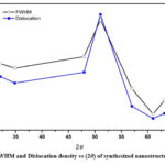 |
Figure 3: FWHM and Dislocation density vs (2θ) of synthesized nanostructure thin film. |
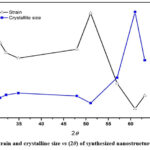 |
Figure 4: Strain and crystallite size vs (2θ) of synthesized nanostructure thin film. |
Scanning Electron Micrograph (SEM) Analysis:
EDX detector connected to SEM was used to measure the surface microstructure and chemical compositions of the deposited nanostructure thin film onto indium doped tin oxide (ITO) coated glass substrate. The SEM micrographs and corresponding elemental mapping of deposited nanostructure ZnO thin films were obtained that was shown in figure (5). The results indicate that the ZnO nanostructures were adherent to the substrate and smoothly deposited by this method. The hexagonal flower like structures were grown in the wide range of 22–70 nm and apparent indication for the formation of nanocrystalline materials in randomly oriented structures with variable size. Zinc Oxide nanostructures were prone to aggregate due to the large surface area and high surface energy.
 |
Figure 5: (a – c) Micrographs and (d – f) Elemental mapping of synthesized ZnO nanostructure. |
UV-Visible Analysis
The absorption spectra of the deposited zinc oxide nanostructure thin films were recorded using UV-Visible spectrometer in the range of 300 to 800 nm which is shown in figure 6(a). The derivative of the absorbance with respect to energy was also obtained and shown in its inset, which also gives the information about the band gap (3.38 eV) of ZnO nanostructure. 20-21In the visible wavelength range the deposited nanostructure thin films show a high optical transmission, which confirms the good optical quality of the structure.
 |
Figure 6(a): UV-visible absorbance spectra of synthesized ZnO nanostructure. |
To verify the above calculated band gap of deposited nanostructure we use other method which is based on the calculation of absorption coefficient (α). The plot of (αhν)2 vs photon energy for the deposited nanostructure thin film was obtained and shown in figure 6(b). The resultant curve was linear throughout a wide range of photon energy, showing that the deposited thin layer was a direct transition material. Tauc’s formula equation (vi) was also used to verify this24

where α, h, ν, C and Eg are the absorption coefficient, Plank’s constant, frequency of incident photon, a constant and the direct transition band gap respectively. The optical band gap was determined by extrapolating the linear portion of the graph (αhν)2 vs hν and shown in figure 6(b).
 |
Figure 6(b): Plot of (αhν)2 vs photon energy (hν) of deposited ZnO nanostructure. |
The calculated band gap from the help of above equation (vi) and extrapolation of the curve was found about 3.34 eV, which is very close measurement to value3.38 eV. The estimated energy band gap shows that the ZnO is suitable candidate for the fabrication of photovoltaic solar cells. The high conductivity and transparency of ZnO nanostructure are important factors for various applications like transparent conducting oxides and TFT etc. For the fabrication of low cost, highly efficient electronic and optoelectronic devices, including transparent conductive films, ZnO nanostructure thin films are the rapidly developing future material.
FTIR Analysis
The presence of organic or inorganic compounds in the deposited nanostructure were identified using Fourier Transform Infrared (FTIR) spectroscopy, which was linked to various functional groups associated with various absorbance peaks in the spectra. Figure (7)shows the FTIR spectra of deposited ZnO nanostructure thin films with transmission peaks ranging from 500 to 4000 cm-1.Figure 7 (a – e) depicts the FTIR spectra of deposited nanostructures at various molarities of aqua solutions containing zinc nitrate (0.1, 0.5, and 1 M) and potassium nitrate (1 M). The variation in FTIR spectra is due to variation in concentration of zinc nitrate. From the above said spectrum, it appears that a strong absorption band at 468.5 cm-1 related to the typical vibration mode of ZnO. A series of peaks were noticed from 500 – 4000 cm-1, with the peak centred at 3307 cm-1corresponding to stretching vibration of intermolecular hydrogen (-OH) bond existing between the adsorbed water molecule and indicating a higher amount of hydroxyl group due to the hygroscopic nature of ZnO.23The presence of sharp peak below 750 cm-1 explains the formation of ZnO bond as well as metal oxide stretches. 26Other functional groups also presented in the sample at various peaks corresponding to -C=O, -C=C etc., which were in the existence due to chemicals presence during the synthesis process of the nanostructure. All of the measured spectra were in good agreement with the reported data for the various molarities of zinc nitrate (0.1, 0.5 and 1 M) and potassium nitrate (1 M) in the initial solution, so it was not much affected the data in FTIR measurements.
 |
Figure 7: FTIR spectra of synthesized ZnO nanostructure. |
Electrical Properties
Keithley Electrometer 6517A was used to measure the current-voltage (I-V) characteristics of deposited ZnO nanostructures thin film, which shows linear behaviour as a function of bias voltage in the range of 1 to 4 volts, as shown in figure (8a).This characteristic behaved linearly in forward and reverse bias voltage up to 1.2 V, indicating an Ohmic contact between the electrodes and thin films of ZnO nanostructure. Infact, ZnO is a direct band gap material in which the electronic configuration of Zn is [Ar]3d104s2 and O is [He]2s22p4. The bottom of the conduction band in a ZnO is caused by occupied 2p states of O2-, while the top of the valence band is caused by empty 4s states of Zn2+. 27The conductivity of deposited thin film depends on carrier concentration, charge mobility, and the current through ZnO nanostructure thin film was a function of Zn2+ concentration16,27, which applied that ZnO is an n-type material for the optoelectronic devices. The following equation describes how conductivity and mobility are related.

where q is the charge on the electron, n is the density of charge carriers in the conduction band, and μ is the mobility of charge carriers. Here some measurements are done with light (visible light: tungsten filament), LED and dark mode. There was a notable change in the LED’s current, but no change in the visible light, as shown by Figures (8a) and its inset figure, which compares the data as plotted on a wider scale. Since ZnO nanostructure can react with environmental oxygen, electronic and optoelectronic devices made from ZnO experience changes in conductivity and electrical properties over time. ZnO-based devices have some instability due to such variation in the electrical properties. After overcoming these technical issues, ZnO based devices can be utilized for both industrial and commercial applications. 28Figure (8b) displays a relatively similar pattern for the current-time profile at even longer times, which was strongly dependent on the applied potential in the device. The resistance of the interface between metal and semiconductor determines the sensitivity in some applications, such as photodetector, and it can be increased under illumination to dark conditions when the interface was Ohmic.29
 |
Figure 8(a): Current-voltage characteristics of synthesized ZnO nanostructure thin film. |
 |
Figure 8(b): Different behaviour of current at various voltages. |
The switching property of the deposited nanostructures was measured and shown in the figure (8c) using the ultra violet (UV lamp B). The plotted data was represented for the switch on and off of UV lamp for 10 seconds each time at voltage 2V. The main goal of this experiment was to investigate how the response behaved over time and how current or resistance changed when the UV lamp was illuminated in the dark for only 10 seconds. The reported findings support that the study was successful in determining the switching property for the gas sensing application. Sinha and others reported that ZnO nanowire has a very high sensitivity for hydrogen (98% to 100 ppm) and CO gas (93% to 200 ppm), with an extremely quick recovery time of 1 to 2 ms. Using standard ZnO nanowire arrays for gas sensor applications, the current transients show the reversible type sensing to reduce gas detection.30Similar findings were taken into consideration for the enhancement of Mg-doped ZnO NPs’ response, which can be related to the contribution of unpaired electrons to the photocurrent. 26, 31According to earlier findings, ZnO or dopped ZnO may be used as a photodetector with a variety of detective wavelengths and may be used as a sensor active material.32
 |
Figure 8(c): Current – time profile at 2V for gas sensing switching properties. |
Conclusion
It has been confirmed that the growth of ZnO nanostructure thin films deposited by a simple two electrode electro-deposition technique from aqua solution of zinc nitrate [0.1, 0.5, 1 M] and potassium nitrate [1 M] solution and were investigated by different characterisation techniques. X-ray diffraction analysis shows that the synthesized ZnO thin films have hexagonal wurtzite structure according to standard ICDD and the crystalline size was calculated as 24.25 nm. SEM micrographs of deposited nanostructures show uniform flower like ZnO structure without any cracks and consisting clusters with star shape and pores. The formation of pores allocated as enhanced growth height that show the roughness of nanostructure thin films. SEM images of deposited thin films demonstrated that the morphology of ZnO nanostructures depend greatly on the potential difference for the depositions. The optical band gap was found to be 3.38 eV. The On-Off switching time is considered for very small period and the main focus was to examine the properties of ZnO nanostructure using current-time profile at different voltages under the dark – illumination of UV lamp. The plotted data in profile show clear evidence to be used for the switching properties in optoelectronic devices. The previous reported data in various results also support our study is good for the gas sensing switching applications.
Acknowledgement
This research work was performed in Department of Physics, University of Rajasthan, Jaipur. The authors are highly thanks to the Director, Centre for Non-Conventional Energy Resources (CNCER), University of Rajasthan, Jaipur for providing measurement and characterization facilities during this experiment.
Conflict of Interest
On behalf of all authors, the corresponding author states that there is no conflict of interest.
References
- Lan, X.; Zhang, J.Y.; Gao, H.; Wang, T.M.CrystEngComm2011, 13,63-636.
CrossRef - Chatterjee,S.; Gohil, S.; Chalke, B.; Ayyub, P. Journal of Nanoscience and Nanotechnology 2009, 9 (8),4792- 4796.
CrossRef - , A.; Kim, M.R.; Chae, Y.S.; Rhee, J.K. Journal of the Korean Physical Society,2009,55 (6),2476-2481
CrossRef - Khelladi, M.R.;Mentar, L.;Beniaiche, A. Journal of Material Science: Mater Electron, 2013, 24, 153–159.
CrossRef - Wang, X.D.; Summers, C.J.; Wang, Z.L. Nano Letters, 2003, 4, 423–427.
CrossRef - Shinde, S.S.; Shinde, P.S.; Oh, Y.W.; Haranath,D.; Bhosale, C.H.; Rajpure, K.Y. Applied Surface Science, 2012, 258, 9969–9976
CrossRef - Ouyang, W.; Teng, F.; He J.H.; Fang, X. Advance Function Materials,2019, 29(9), 1807672(1-20).
CrossRef - Shishiyanu, S.T.; Shishiyanu T.S.; Lupan, O.I.2005, Sensors Actuators B: Chemical, 107, 379-386.
CrossRef - Batra, N.; Tomar M.; Gupta, V.2012, J.Appl. Phys, 112, 114701(1-6).
CrossRef - Rogers,D. J.; Teherani,F. H.; Yasan, A.; Minder, K.; Kung P.; Razeghi, M. Journal of Applied Physics Letters, 2006, 6474, 64740(Q1-Q6).
- Ali, G.M.; Chakrabarti, P. IEEE Photonics Journal, 2010, 2(5), 784-793.
CrossRef - Zhu, J.;Li, H.; Wang, L.; Hu, Y.; Jiang, B.; Hi, Y. Applied Thermal Engineering, 2015, 88, 363-368.
CrossRef - Consonni, V.; Rey, G.; Bonaime G.; Karst, N.; Doisneau B.Applied Physics Letters, 2011, 98, 111906(1-3).
CrossRef - Muchuweni, E.; Sathiaraj, T.S.; Nyakotyo, H.Heliyon 2017, 3, e00285(1-18).
CrossRef - Srivastava, A.K.; Kumar, J. Science and Technology of Advanced Materials, 2013, 14(6), 065002(1-15).
CrossRef - Yoshida, T.; Komatsu, D.; Shimokawa,N.; Minoura, H. Thin Solid Films, 2004,451, 166–169.
CrossRef - Taleatu, B.A.; Fasisi, A.Y.; Santo, G.Di.; Bernstorff, S.; Goldoni, A.; Fanetti, M.; Floreano, N.; Borghetti, P.; Casalis, L.; Sanavio, B. Castellarin Cudia, C., AIP advances 2011, 1, 032147 (1-10).
CrossRef - Lasisi, A.R.; Alabi, A.B.; Taleatu, B.A.; Babalola, O.A.Ife. Journal of Science, 2021,23(2),035-042.
CrossRef - Sonawane, B.K.; Bhole, M.P.; Patil, D.S. Physica B: Condensed Matter 2010, 405, 1603–1607.
CrossRef - Abdulrahman, A.F.; Ahmed, S.M.; Ahmed, N.M. Science Journal of University of Zakho, 2017, 5(1), 128-135.
CrossRef - Abdulrahman, A.F. Journal of Materials Science: Materials in Electronics, 2020, 31, 14357–14374.
CrossRef - Calhoun, R.B.; Dunand, David C. Material Science and Engineering,2020, 3, 27-59.
- Tauc,J.; Grigorovici, R.;Vancu, A. Basic Solid State Physics,1966,15,627–637.
CrossRef - Roy, S.; Das, S.; Sarkar, C.K. International Nano Letters,2016, 6, 199–210.
CrossRef - Sharma, S.; Yadav, D.K.; Chawla, K.; Lal, N.; Lal, C. International Journal of Recent Research and Review, 2021, XIV(2), 1-6.
- Klingshirn, C.F.Springer Series in Materials Science book series,2010, 120, 325-345.
CrossRef - Vyas, S.Johnson Matthey Technology Review,2020, 64(2), 202–218.
CrossRef - Yoon, Y.J.; Park, K.S.; Heo, J.H.; Park, J.G.; Nahm, S.; Choi, K.J.Journal of Material Chemistry,2010,20, 2386-2390.
CrossRef - Sinha, M.;Mahapatra, R.; Mondal, B.;Maruyama, T.;Ghosh, R. Journal of Physical Chemistry C,2016, 120(5), 3019–3025.
CrossRef - Hasan, K.; Alvi, N.H.; Lu, J.; Nur, O.;Willander, M. Nanoscale Research Letters,2011,6(348), 1-6.
CrossRef - Kind, H.; Yan, H.; Messer, B.; Law, M.;Yang, P. Advanced Materials,2002,14(2), 158–160.
CrossRef

This work is licensed under a Creative Commons Attribution 4.0 International License.
About The Author
![]()
A New Edition of Web of Science
Journal Impact Factor
2022: 0.5
Five Year: 0.8
Journal is Indexed in

Cabells Whitelist
![]()


