Article

Static Hydrophobic Cuprous Oxide Surface Fabricated via One-Step Laser-Induced Oxidation of a Copper Substrate

1
Institute of Materials and Systems for Sustainability, Nagoya University, Nagoya 464-8603, Japan
2
Department of Engineering, Nagoya Institute of Technology, Nagoya 466-8555, Japan
3
Graduate School of Engineering, Nagoya University, Nagoya 464-8603, Japan
*
Author to whom correspondence should be addressed.
Micromachines 2023, 14(1), 185; https://doi.org/10.3390/mi14010185
Submission received: 9 December 2022 / Revised: 29 December 2022 / Accepted: 9 January 2023 / Published: 11 January 2023
(This article belongs to the Special Issue Ultrafast Laser Micro- and Nanoprocessing)

Abstract

:
In this study, we developed a one-step method for fabricating hydrophobic surfaces on copper (Cu) substrates. Cuprous oxide (Cu2O) with low free energy was successfully formed after low-fluence laser direct irradiation. The formation of Cu2O enhanced the hydrophobicity of the Cu substrate surface, and the contact angle linearly increased with the proportion of Cu2O. The Cu2O fabricated by low-fluence laser treatment showed the same crystal plane orientation as the pristine Cu substrate, implying an epitaxial growth of Cu2O on a Cu substrate.

1. Introduction

Cuprous oxide (Cu2O) and copper oxide (CuO) have been investigated for photovoltaic applications [1,2,3,4,5] owing to their feasible bandgap (1.9–2.2 and 1.2–1.7 eV, respectively) corresponding to the visible region. Cu2O is also an emerging photocathode for water splitting [6,7,8]. However, there is still a need to develop low-cost methods for preparing high-quality and large-scale crystals of these promising materials [9,10,11,12,13,14]. It is more feasible to fabricate copper oxide complex thin films, which have been achieved on copper (Cu) layers via thermal oxidation for solar cells [15] and laser processing for photodetectors and glucose sensing [16,17]. Laser-treated Cu-substrate surfaces with controllable wettability have also been reported. Long et al. treated laser-fabricated microstructures with CF3(CF2)7CF2CF2−Si−(OCH3)3 methanol [18], triethoxyoctylsilane [19], and fluoroalkylsilane [20] to reduce their surface free energy. Pan et al. soaked laser-textured microstructures in a stearic acid solution at ambient temperature for 60 min and dried them in an oven (60 °C) for 10 min to achieve low-adhesive features [21]. He et al. treated laser-fabricated microstructures with ethanol-assisted low-temperature annealing [22], and Ma et al. heated similar structures [23] to transform hydrophilic CuO to hydrophobic Cu2O and form hydrophobic organics. In these studies, the wettability and morphology of laser-fabricated microstructures have been extensively studied, and postprocessing was needed to add the hydrophobic base to the surface. It is also reported that a lower oxygen amount of copper-oxidation surface is associated with lower surface energy, leading to an increase in hydrophobicity [24]. Cu2O surfaces have been fabricated by chemical bath deposition [24] and electrodeposition [25,26] for achieving a hydrophobic surface. In our previous study, we developed a one-step patterning oxidation method for Cu surfaces via femtosecond laser irradiation in the atmosphere [27]. The high peak fluence due to the ultrashort pulse duration promoted the chemical reaction between Cu and oxygen. To avoid the formation of structures in the micrometer order, the samples were treated under low average fluence to suppress laser ablation. Using this one-step surface modification method, we fabricated a Cu2O layer with a thickness of less than 30 nm on the surface of a Cu substrate. Without any postprocessing, the one-step laser-treated surface showed enhanced hydrophobic features owing to the formation of low-free-energy Cu2O. In addition to improving the useful time of Cu-based machine parts due to the self-cleaning feature of hydrophobic surfaces, this one-step laser-induced Cu2O surface also showed some potential applications, such as biocides [28], photovoltaic devices [29], and photocatalysts [6].

2. Materials and Methods

To determine the laser processing threshold of Cu substrates (113513, Nilaco, Japan), femtosecond laser pulses (wavelength: 1030 nm, pulse width: 700 fs, repetition rate: 100 kHz, PHAROS PH1–10, Light Conversion, Vilnius, Lithuania) with pulse energy of 5–60 μJ were focused and irradiated on a Cu substrate surface. The area of the single-pulse irradiated spots was measured by confocal laser scanning microscopy (CLSM, LEXT ILS4100, Olympus, Tokyo, Japan) to calculate the ablation threshold energy of Cu. Before fabricating hydrophobic samples with a large area, two 0.5 mm × 0.5 mm samples on Cu substrates were fabricated with low laser fluence. Their surface morphologies were evaluated by scanning electron microscopy (SEM, JSM-5600, JEOL, Tokyo, Japan), and their surface oxidation state was confirmed by Raman spectra (Nanofinder FLEX, TII, Tokyo, Japan). The thickness of oxidation layers was evaluated by scanning transmission electron microscopy and energy dispersive X-ray spectrometry (STEM-EDX, JEM-2100F/HK, JEOL, Tokyo, Japan). Based on the initial experimental results, samples with a size of 4 mm × 4 mm were fabricated by low-fluence laser irradiation. The surface roughness was measured by an atomic force microscope (AFM, JSPM-5200TM, JEOL, Tokyo, Japan). X-ray patterns (XRD, SmartLab, Rigaku, Tokyo, Japan), and the contact angle (CA, Smart Contact PRO 100, Excimer Inc., Yokohama, Japan) of these samples were also measured to investigate the relationship between their surface chemical composition and hydrophobicity.

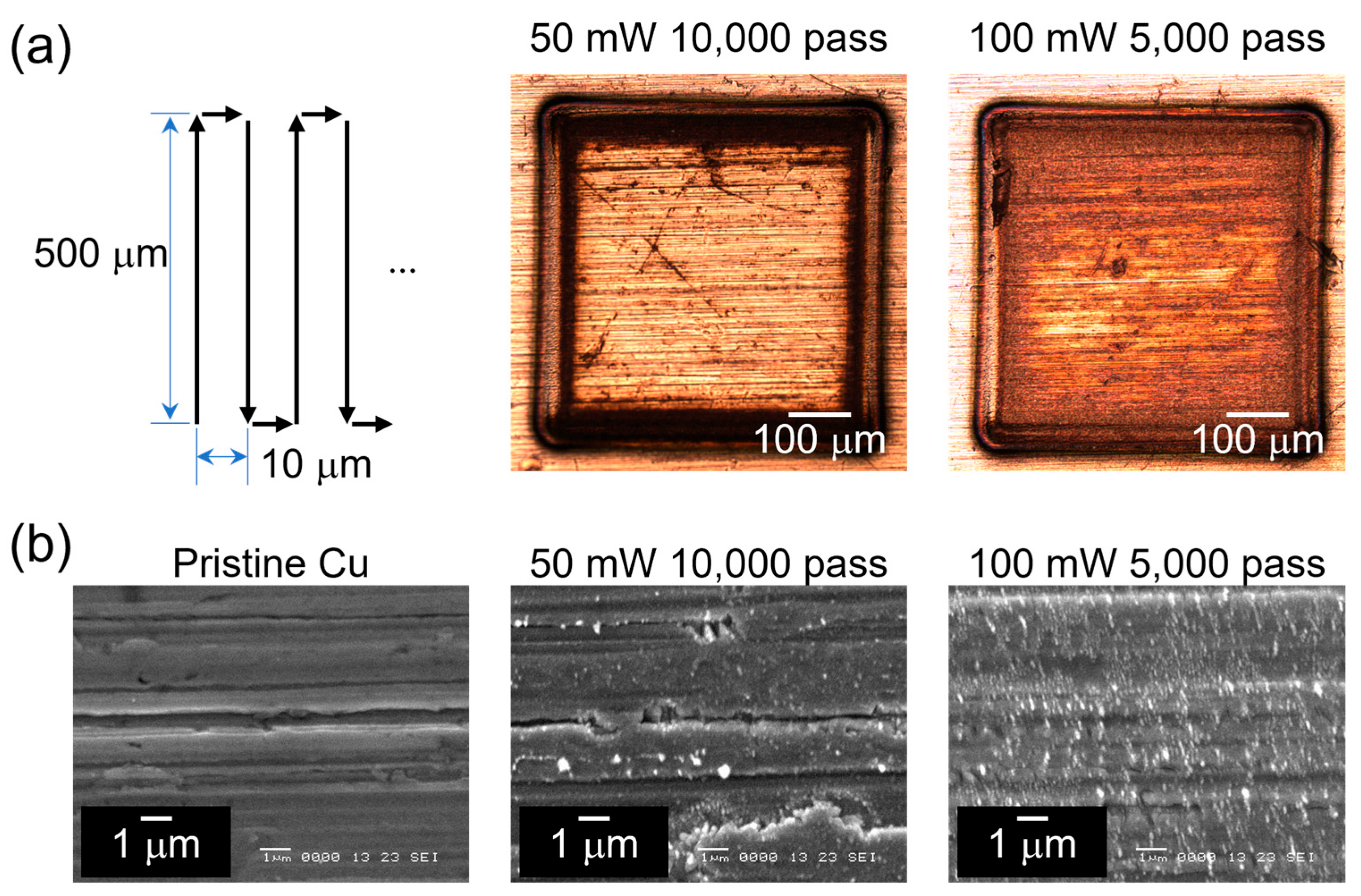
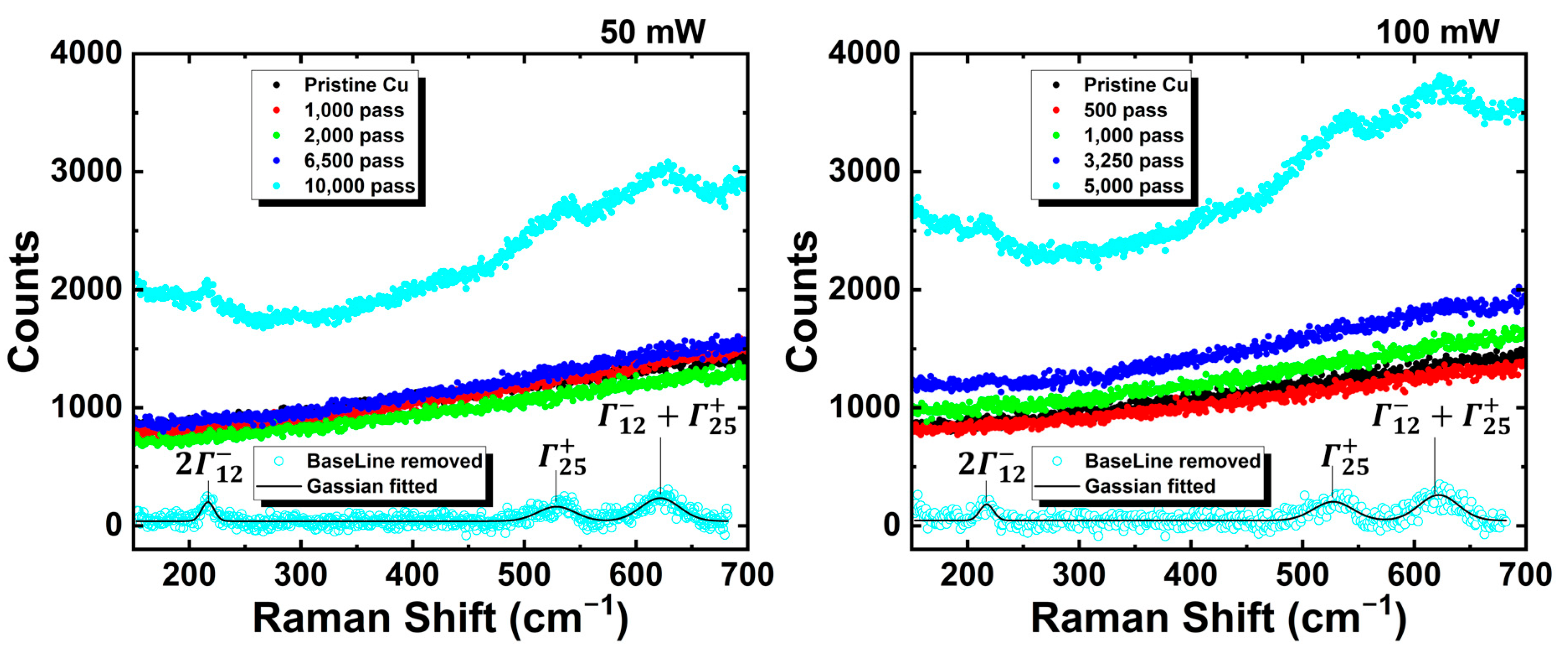
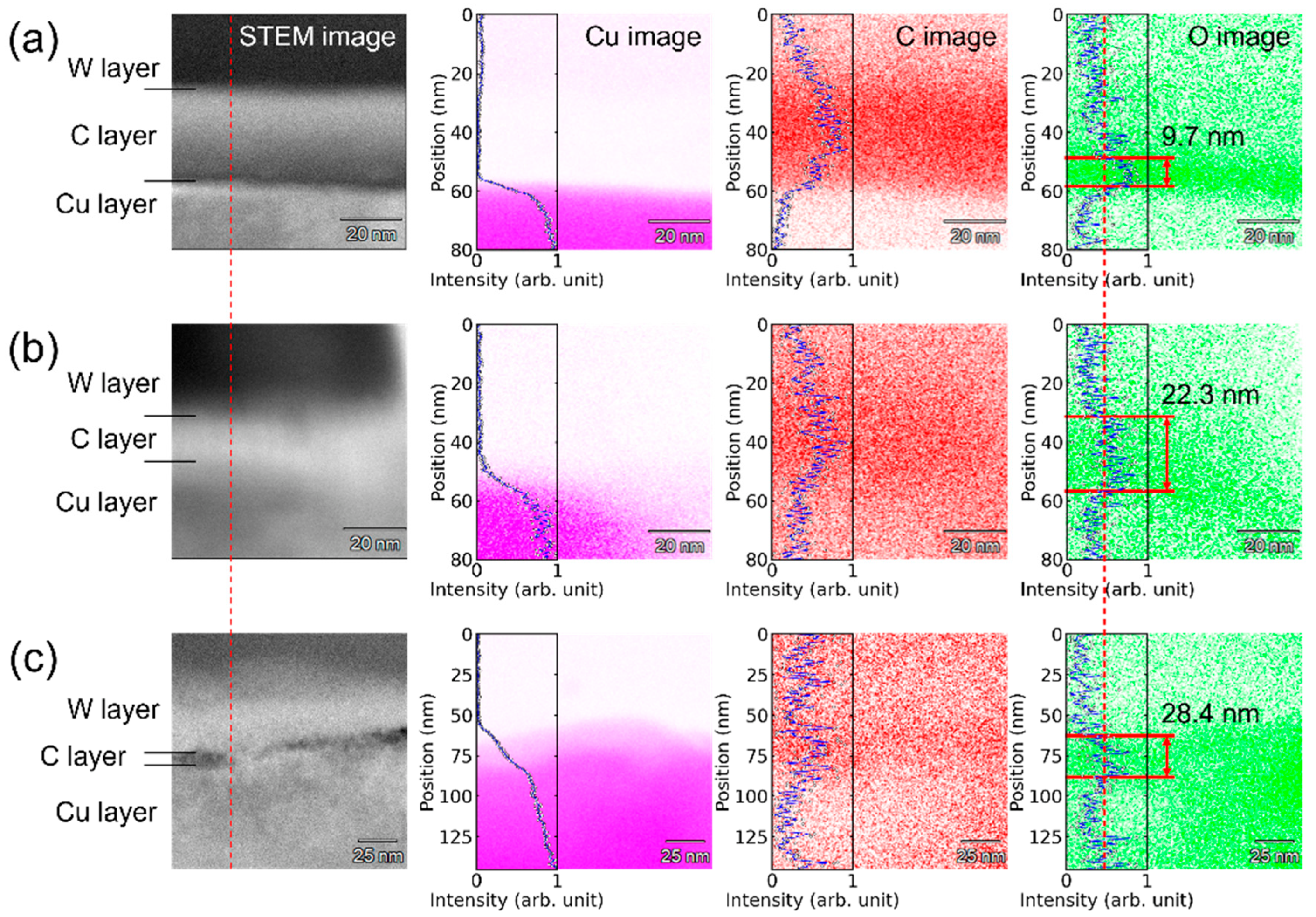
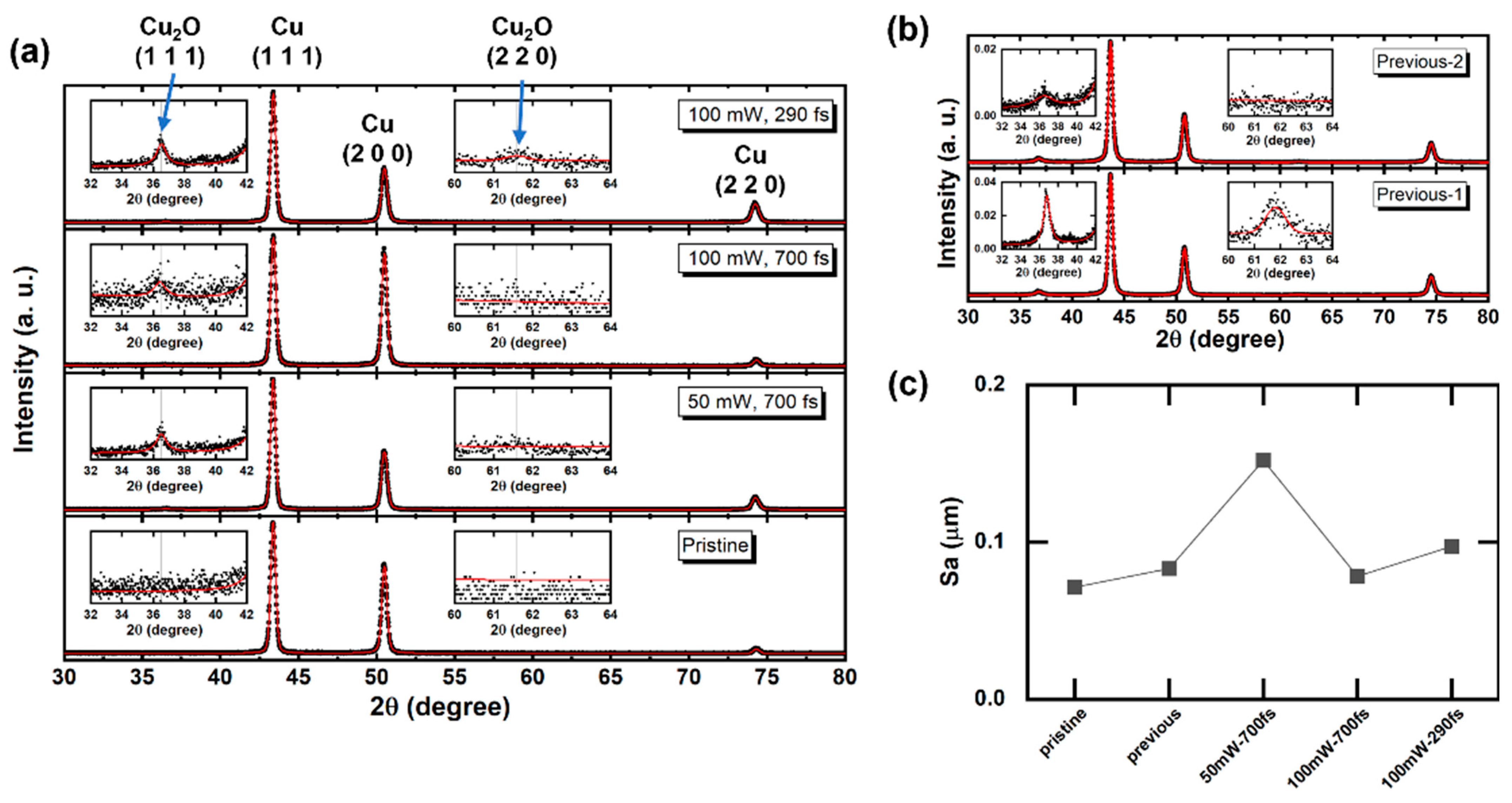
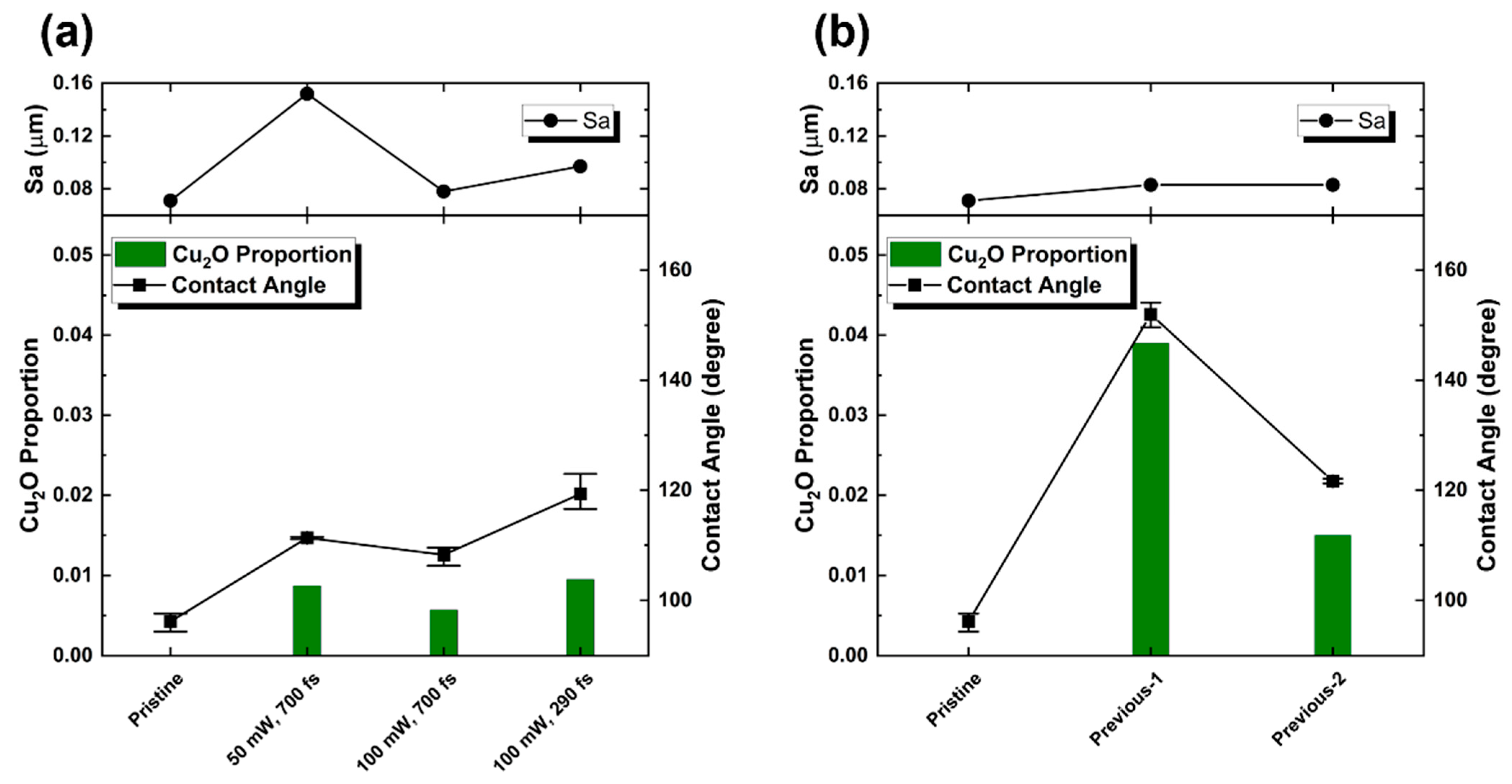
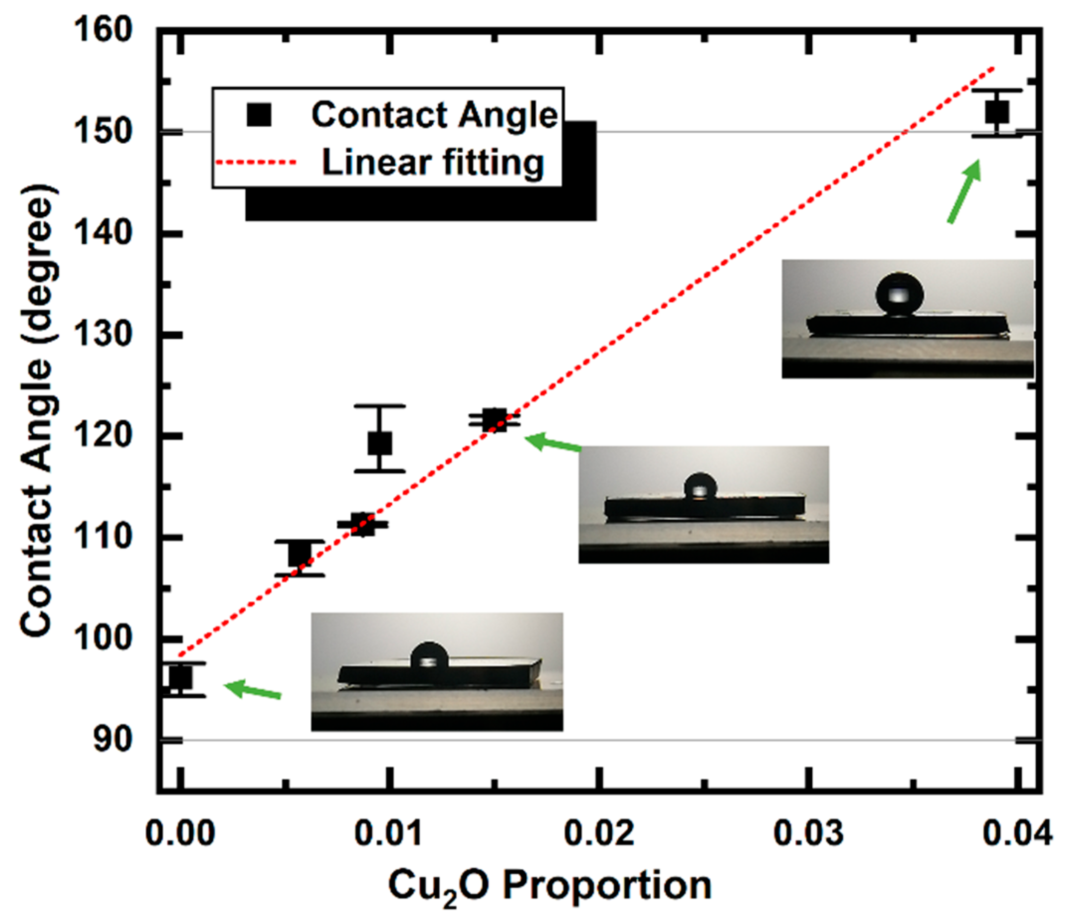
3. Results and Discussion

Figure 1 shows the spot diameter square (D2) as a function of pulse energy (Epulse). The measured D2 was fitted to D 2 = 2 ω 0 2 ln E pulse E th , where Eth is the ablation threshold energy, and the slope of the fitting is the beam radius at the surface (ω0) [30]. According to the fitting result, Eth is 5.1 μJ, and ω0 is 19.9 μm. When the pulse energy is less than Eth (5.1 μJ), the irradiated area shows no visible discoloration in the CLSM image. The 0.5 mm × 0.5 mm samples were irradiated by femtosecond laser pulses with an Epulse of 0.5 μJ (50 mW at a 100 kHz repetition rate) and 1 μJ (100 mW at a 100 kHz repetition rate), which are much lower than Eth. Laser-induced plasma was not observed during the laser irradiation. The scanning patterns and their images are shown in Figure 2a. The laser beam was guided using a galvanometer scanner head, and the scan speed was 1000 mm/s with respect to the substrate surface. The scanning line space is 10 μm. The 100 mW-irradiated area showed a more pronounced discoloration than the 50 mW-irradiated area, even though they were treated with the same total input energy. Figure 2b shows the SEM image of the pristine and laser-irradiated areas. Instead of the general microstructure fabricated by laser ablation, the low-fluence-treated surfaces showed nanoprotuberances. Mori et al. reported similar nanoprotuberances on a plasma-treated Cu surface, and they also confirmed the formation of the Cu1+ on the Cu surface with these nanostructures [31]. The pristine Cu showed brushing trenches on the surface, and these trenches remained after the low-fluence irradiation.
Figure 3 shows the Raman spectra of the low-fluence-treated Cu surface. The solid dots indicate the measured results. The hollow dots show the baseline-removed Raman spectrum [32], and the black line is Gaussian-fitted results from the baseline-removed Raman spectrum. Three peaks were observed for the 10,000- and 5000-pass-treated samples. Based on the fitting results, the three peaks at 216, 524, and 625 cm−1 are attributed to Cu2O for the second-order overtone of the silent Γ 12 mode, the Raman-active Γ 25 + mode, and the combination mode of Γ 12 + Γ 25 + [33,34,35,36,37], respectively. To confirm the crystallinity of the laser-irradiated area, we cross-sectionally picked up thin specimens from the irradiated center of the 500 μm × 500 μm samples using the focused ion beam (FIB) technique (Hitachi FB2100, Japan) and evaluated them by STEM-EDX. It is difficult to identify the type of oxidation based on the measured lattice space because those of Cu, Cu2O, and CuO are very close. EDX element mapping showed the thickness of the oxidized layer (Figure 4). Based on the mapping results, oxygen (O) layers were sandwiched between the carbon (C) and Cu layers, indicating that the oxygen was on the Cu surface before the FIB processing. A 9.7 nm-thick O layer due to natural oxidation was observed on the surface of the pristine Cu substrate. Its thickness increased by more than two times for the 50 mW-irradiated surface and three times on the surface of the 100 mW-irradiated surface. The thickness of the O layer was facilitated by laser irradiation, and higher power resulted in thicker oxidation layers owing to the longer laser penetration lengths.
Table 1 shows the fabrication conditions and experiment date of laser processing, XRD, and contact angle measurement. Three samples (current samples in Table 1) with a 4 mm × 4 mm area (scanning line space: 10 μm, laser wavelength: 1030 nm, repetition rate: 100 kHz) were fabricated to evaluate the relationship between their wettability and surface oxidation conditions, and a sample from our previous study (previous sample in Table 1, fabricated using another laser with a wavelength of 1045 nm, a pulse duration of 700 fs, and a repetition rate of 100 kHz at 25 mW) [27] was also evaluated.
Figure 5a,b show the XRD pattern of the laser-irradiated Cu surfaces. The black dots indicate the measured data, and the red lines show the PseudoVoigt function fitting results [38,39]. Compared with the pristine Cu surface, a peak attributed to Cu2O (1 1 1) with a lattice spacing (d) of 2.09 Å was observed for all laser-irradiated samples. In Figure 5b, the Previous-1 and Previous-2 are XRD patterns with different measurement dates for the same sample from our previous work. Additionally, the Previous-1 XRD pattern shows a peak attributed to Cu2O (2 2 0) (d: 1.28 Å). The orientation of (2 2 0) was also observed for the pristine Cu substate. Compared with the monoclinic structure of CuO, Cu2O has the same cubic structure as Cu, which may promote the growth of Cu2O on a Cu substrate. Barton et al. [40] reported epitaxial electrodeposition of Cu2O on single-crystal Cu owing to the similar cubic cell structures of Cu2O and Cu. They also reported that an epitaxial-grown Cu2O (2 0 0) (d: 1.81 Å) thin film on Cu (2 0 0) (d: 2.13 Å) has a thickness limitation. On a Cu (2 0 0) substrate, Cu2O (1 1 1) first grows instead of Cu2O (2 0 0), and Cu2O (2 0 0) appears when the film is thicker than 360 nm. Previous-2 showed a weaker Cu2O (1 1 1) peak than that of Previous-1 and no Cu2O (2 2 0) peak. This weakening of the Cu2O peak can be attributed to the natural oxidation of Cu2O to CuO, and the increased proportion of CuO was too low to be detected by XRD. Kwon et al. [16] reported that CuO was formed in the laser ablation center; in contrast, Cu2O was formed in the surrounding where it has lower energy density, i.e., laser fluence, than that of the center due to the Gaussian distribution of fluence. In the laser-irradiated spot, the fluence distribution determines the temperature distribution, thus determining the type of formed oxide. Lower fluence is associated with lower temperature, which facilitates the formation of Cu2O. Consequently, the low-fluence treatment in this study favored Cu2O formation. The arithmetical mean height (Sa) was used to evaluate the surface roughness as shown in Figure 5c. Sa increased less than 0.1 μm when irradiated by low laser fluence.
Figure 6 plots the CA, Sa, and Cu2O proportion of the pristine and laser-irradiated samples. The Cu2O proportion was obtained from the ratio of the peak area (PseudoVoigt function fitting) attributed to Cu2O to that of Cu. In Figure 6a, the Sa increased by less than 0.1 μm, and in Figure 6b the Sa is almost kept the same for the pristine and the previous sample. The low-fluence laser-treated samples did not change too much in the surface roughness, which cannot significantly change the CA [25,41]. On the contrary, the proportion of Cu2O showed a positive correlation to the CAs. These results suggest that the surface free energy will be dominant to the static CA when the surface roughness insignificantly changes. Figure 7 shows the relationship between the Cu2O proportion and CA of the samples. CA increased linearly with the Cu2O proportion. The oxidation of metal copper may mitigate the surface free energy of pristine Cu, consequently enhancing the surface hydrophobicity. Meanwhile, a lower amount of oxygen results in lower surface energy [24], and Cu2O facets show different surface energies: E111 < E110 < E100 [42], i.e., Cu2O (1 1 1) exhibits higher hydrophobicity than other faces. In the report of Kwon et al. [43], Cu2O showed the largest CA than that of Cu and CuO due to their different interparticle bonds [44]. These results suggest that, besides the surface structure in micro-order, the chemical composition is an important factor determining the wettability of the surface. In addition, hydrophobicity is controllable by this simple method because surface chemical compositions can be controlled by varying the laser conditions to create different reaction conditions and atmospheres.

4. Conclusions

In conclusion, via one-step laser irradiation, we fabricated hydrophobic surfaces on Cu substrates owing to the formation of low-free-energy Cu2O. The temperature of a laser-irradiated area could be adjusted by controlling the laser fluence, which determines the chemical composition of the copper oxides. The CA of the Cu surface exhibited enhanced hydrophobicity after the simple one-step process, showing a linear increase in the Cu2O proportion. The laser-induced Cu2O showed the same plane orientation as the Cu substrate owing to their similar cubic cell structures, implying an epitaxial growth of Cu2O on Cu. This simple one-step technique can promote the application of laser-induced functional surfaces and demonstrates the potential of laser-assisted epitaxial growth of metal oxides via direct laser irradiation in the atmosphere.

Author Contributions

Conceptualization, X.Y. and S.O.; methodology, X.Y., T.K., T.I., M.K.; software, X.Y.; validation, X.Y., T.K.; formal analysis, X.Y.; investigation, X.Y., Y.T., T.K., and T.I.; resources, X.Y., K.S., M.K., F.I. and S.O.; data curation, X.Y.; writing—original draft preparation, X.Y.; writing—review and editing, all the authors; visualization, X.Y.; supervision, M.K. and S.O.; project administration, M.K. and S.O.; funding acquisition, X.Y., F.I., M.K. and S.O. All authors have read and agreed to the published version of the manuscript.

Funding

This study was sponsored by KAKENHI (Grant No. 21H04637); Amada Foundation (Grant No. AF-2019213-B2); Iketani Science and Technology Foundation (Grant No. 0341176-A); Strategic Foundational Technology Improvement Support Operation; Grants-in-aid for the Program for Building Regional Innovation Ecosystem “Aichi Innovation Ecosystem Project for Next-Generation Automobile” from the Ministry of Education, Culture, Sports, Science and Technology of Japan; Osawa Scientific Studies Grants Foundation; Hirose Foundation.

Data Availability Statement

The data that support the findings of this study are available from the corresponding author upon reasonable request.

Conflicts of Interest

The authors declare no conflict of interest associated with this manuscript.

References

  1. Papadimitriou, L.; Economou, N.A.; Trivich, D. Heterojunction Solar Cells on Cuprous Oxide. Sol. Cells 1981, 3, 73–80. [Google Scholar] [CrossRef]
  2. Michael, J.J.; Iniyan, S. Performance Analysis of a Copper Sheet Laminated Photovoltaic Thermal Collector Using Copper Oxide–Water Nanofluid. Sol. Energy 2015, 119, 439–451. [Google Scholar] [CrossRef]
  3. Rakhshani, A.E. Preparation, Characteristics and Photovoltaic Properties of Cuprous Oxide—A Review. Solid-State Electron. 1986, 29, 7–17. [Google Scholar] [CrossRef]
  4. Chandrasekaran, S. A Novel Single Step Synthesis, High Efficiency and Cost Effective Photovoltaic Applications of Oxidized Copper Nano Particles. Sol. Energy Mater. Sol. Cells 2013, 109, 220–226. [Google Scholar] [CrossRef]
  5. Zuo, C.; Ding, L. Solution-Processed Cu2O and CuO as Hole Transport Materials for Efficient Perovskite Solar Cells. Small 2015, 11, 5528–5532. [Google Scholar] [CrossRef]
  6. Hara, M.; Kondo, T.; Komoda, M.; Ikeda, S.; Kondo, J.N.; Domen, K.; Hara, M.; Shinohara, K.; Tanaka, A. Cu2O as a Photocatalyst for Overall Water Splitting under Visible Light Irradiation. Chem. Commun. 1998, 2, 357–358. [Google Scholar] [CrossRef]
  7. Bagal, I.V.; Chodankar, N.R.; Hassan, M.A.; Waseem, A.; Johar, M.A.; Kim, D.-H.; Ryu, S.-W. Cu2O as an Emerging Photocathode for Solar Water Splitting—A Status Review. Int. J. Hydrogen Energy 2019, 44, 21351–21378. [Google Scholar] [CrossRef]
  8. de Jongh, P.E.; Vanmaekelbergh, D.; Kelly, J.J. Cu2O: A Catalyst for the Photochemical Decomposition of Water? Chem. Commun. 1999, 1069–1070. [Google Scholar] [CrossRef]
  9. Mall, A.K.; Kumar, P.; Garg, A.; Gupta, R. Synthesis, Growth, and Characterizations of CuO Single Crystal. In Proceedings of the AIP Conference Proceedings, Bikaner, India, 24–25 November 2017; Volume 1953, p. 070008. [Google Scholar]
  10. Bush, A.A.; Shkuratov, V.Y.; Kuz’menko, A.B.; Tishchenko, E.A. Growth and Morphological Study of Copper Oxide Single Crystals. Crystallogr. Rep. 2002, 47, 335–339. [Google Scholar] [CrossRef]
  11. Papadimitriou, L.; Economou, N.A. Preparation of Bulk Single Crystals of Cu2O by the Plastic Flow Method and Investigation of Their Electrical Properties. J. Cryst. Growth 1983, 64, 604–608. [Google Scholar] [CrossRef]
  12. Ebisuzaki, Y. Preparation of Monocrystalline Cuprous Oxide. J. Appl. Phys. 1961, 32, 2027–2028. [Google Scholar] [CrossRef]
  13. Toth, R.S.; Kilkson, R.; Trivich, D. Preparation of Large Area Single-Crystal Cuprous Oxide. J. Appl. Phys. 1960, 31, 1117–1121. [Google Scholar] [CrossRef]
  14. Su, M.; Liang, Z.; Zhao, C.; Liu, P.; Yue, S.; Xie, W. Preparation of High Quality Cu2O Crystal and Its Opto-Electronic Properties. Mater. Lett. 2016, 170, 80–84. [Google Scholar] [CrossRef]
  15. Chen, L.-C.; Chen, C.-C.; Liang, K.-C.; Chang, S.H.; Tseng, Z.-L.; Yeh, S.-C.; Chen, C.-T.; Wu, W.-T.; Wu, C.-G. Nano-Structured CuO-Cu2O Complex Thin Film for Application in CH3NH3PbI3 Perovskite Solar Cells. Nanoscale Res. Lett. 2016, 11, 402. [Google Scholar] [CrossRef] [Green Version]
  16. Kwon, H.; Kim, J.; Ko, K.; Matthews, M.J.; Suh, J.; Kwon, H.J.; Yoo, J.H. Laser-Induced Digital Oxidation for Copper-Based Flexible Photodetectors. Appl. Surf. Sci. 2021, 540, 148333. [Google Scholar] [CrossRef]
  17. Sedaghat, S.; Nejati, S.; Bermejo, L.H.; He, Z.; Alcaraz, A.M.; Roth, A.; Li, Z.; Pol, V.G.; Wang, H.; Rahimi, R. Laser-Induced Atmospheric Cu: XO Formation on Copper Surface with Enhanced Electrochemical Performance for Non-Enzymatic Glucose Sensing. J. Mater. Chem. C 2021, 9, 14997–15010. [Google Scholar] [CrossRef]
  18. Long, J.; Fan, P.; Gong, D.; Jiang, D.; Zhang, H.; Li, L.; Zhong, M. Superhydrophobic Surfaces Fabricated by Femtosecond Laser with Tunable Water Adhesion: From Lotus Leaf to Rose Petal. ACS Appl. Mater. Interfaces 2015, 7, 9858–9865. [Google Scholar] [CrossRef]
  19. Long, J.; Fan, P.; Zhong, M.; Zhang, H.; Xie, Y.; Lin, C. Superhydrophobic and Colorful Copper Surfaces Fabricated by Picosecond Laser Induced Periodic Nanostructures. Appl. Surf. Sci. 2014, 311, 461–467. [Google Scholar] [CrossRef]
  20. Long, J.; Pan, L.; Fan, P.; Gong, D.; Jiang, D.; Zhang, H.; Li, L.; Zhong, M. Cassie-State Stability of Metallic Superhydrophobic Surfaces with Various Micro/Nanostructures Produced by a Femtosecond Laser. Langmuir 2016, 32, 1065–1072. [Google Scholar] [CrossRef]
  21. Pan, Q.; Sun, B.; Liu, W.; Xue, W.; Cao, Y. Hyper Gyrating Droplets Generated on a Selective Laser Textured Heterogeneous Wettability Surface. Langmuir 2020, 36, 8123–8128. [Google Scholar] [CrossRef]
  22. He, A.; Liu, W.; Xue, W.; Yang, H.; Cao, Y. Nanosecond Laser Ablated Copper Superhydrophobic Surface with Tunable Ultrahigh Adhesion and Its Renewability with Low Temperature Annealing. Appl. Surf. Sci. 2018, 434, 120–125. [Google Scholar] [CrossRef]
  23. Ma, L.; Wang, L.; Li, C.; Guo, J.; Shrotriya, P.; Deng, C.; Zhao, J. Hybrid Nanosecond Laser Processing and Heat Treatment for Rapid Preparation of Super-Hydrophobic Copper Surface. Metals 2019, 9, 668. [Google Scholar] [CrossRef] [Green Version]
  24. Akbari, R.; Mohammadizadeh, M.R.; Khajeh Aminian, M.; Abbasnejad, M. Hydrophobic Cu2O Surfaces Prepared by Chemical Bath Deposition Method. Appl. Phys. A 2019, 125, 190. [Google Scholar] [CrossRef]
  25. Akbari, R.; Ramos Chagas, G.; Godeau, G.; Mohammadizadeh, M.; Guittard, F.; Darmanin, T. Intrinsically Water-Repellent Copper Oxide Surfaces; An Electro-Crystallization Approach. Appl. Surf. Sci. 2018, 443, 191–197. [Google Scholar] [CrossRef]
  26. Zhao, W.; Fu, W.; Yang, H.; Tian, C.; Li, M.; Li, Y.; Zhang, L.; Sui, Y.; Zhou, X.; Chen, H.; et al. Electrodeposition of Cu2O Films and Their Photoelectrochemical Properties. CrystEngComm 2011, 13, 2871. [Google Scholar] [CrossRef]
  27. Yu, X.; Sudo, M.; Itoigawa, F.; Ono, S. Patterning Oxidation via Femtosecond Laser Irradiation on Copper Substrate. In Proceedings of the Conference on Lasers and Electro-Optics/Pacific Rim, Hong Kong, China, 29 July–3 August 2018; OSA: Washington, DC, USA, 2018; p. W3A.93. [Google Scholar]
  28. Thomas, K.; Raymond, K.; Chadwick, J.; Waldock, M. The Effects of Short-term Changes in Environmental Parameters on the Release of Biocides from Antifouling Coatings: Cuprous Oxide and Tributyltin. Appl. Organomet. Chem. 1999, 13, 453–460. [Google Scholar] [CrossRef]
  29. Sears, W.M.; Fortin, E. Preparation and Properties of Cu2O/Cu Photovoltaic Cells. Sol. Energy Mater. 1984, 10, 93–103. [Google Scholar] [CrossRef]
  30. Yu, X.; Itoigawa, F.; Ono, S. Femtosecond Laser-Pulse-Induced Surface Cleavage of Zinc Oxide Substrate. Micromachines 2021, 12, 596. [Google Scholar] [CrossRef]
  31. Mori, H.; Sakakibara, A.; Itoigawa, F. Fine Protrusion Formation on Copper Substrate Using Atmospheric-Pressure Plasma Treatment. J. Surf. Finish. Soc. Jpn. 2019, 70, 471–476. [Google Scholar] [CrossRef] [Green Version]
  32. Zhang, Z.-M.; Chen, S.; Liang, Y.-Z. Baseline Correction Using Adaptive Iteratively Reweighted Penalized Least Squares. Analyst 2010, 135, 1138. [Google Scholar] [CrossRef]
  33. Gao, H.; Zhang, J.; Li, M.; Liu, K.; Guo, D.; Zhang, Y. Evaluating the Electric Property of Different Crystal Faces and Enhancing the Raman Scattering of Cu2O Microcrystal by Depositing Ag on the Surface. Curr. Appl. Phys. 2013, 13, 935–939. [Google Scholar] [CrossRef]
  34. Yu, P.Y.; Shen, Y.R. Resonance Raman Studies in Cu2O. I. The Phonon-Assisted 1s Yellow Excitonic Absorption Edge. Phys. Rev. B 1975, 12, 1377–1394. [Google Scholar] [CrossRef]
  35. Yu, P.Y.; Shen, Y.R. Multiple Resonance Effects on Raman Scattering at the Yellow-Exciton Series of Cu2O. Phys. Rev. Lett. 1974, 32, 373–376. [Google Scholar] [CrossRef]
  36. Compaan, A.; Cummins, H.Z. Resonant Quadrupole-Dipole Raman Scattering at the 1S Yellow Exciton in Cu2O. Phys. Rev. Lett. 1973, 31, 41–44. [Google Scholar] [CrossRef]
  37. Yu, P.Y.; Shen, Y.R.; Petroff, Y.; Falicov, L.M. Resonance Raman Scattering at the Forbidden Yellow Exciton in Cu2O. Phys. Rev. Lett. 1973, 30, 283–286. [Google Scholar] [CrossRef]
  38. Sánchez-Bajo, F.; Cumbrera, F.L. The Use of the Pseudo-Voigt Function in the Variance Method of X-ray Line-Broadening Analysis. J. Appl. Crystallogr. 1997, 30, 427–430. [Google Scholar] [CrossRef]
  39. Enzo, S.; Fagherazzi, G.; Benedetti, A.; Polizzi, S. A Profile-Fitting Procedure for Analysis of Broadened X-ray Diffraction Peaks. I. Methodology. J. Appl. Crystallogr. 1988, 21, 536–542. [Google Scholar] [CrossRef]
  40. Barton, J.K.; Vertegel, A.A.; Bohannan, E.W.; Switzer, J.A. Epitaxial Electrodeposition of Copper(I) Oxide on Single-Crystal Copper. Chem. Mater. 2001, 13, 952–959. [Google Scholar] [CrossRef]
  41. Li, C.; Zhang, J.; Han, J.; Yao, B. A Numerical Solution to the Effects of Surface Roughness on Water–Coal Contact Angle. Sci. Rep. 2021, 11, 459. [Google Scholar] [CrossRef]
  42. Maimaiti, Y.; Nolan, M.; Elliott, S.D. Reduction Mechanisms of the CuO(111) Surface through Surface Oxygen Vacancy Formation and Hydrogen Adsorption. Phys. Chem. Chem. Phys. 2014, 16, 3036. [Google Scholar] [CrossRef]
  43. Kwon, M.H.; Jee, W.Y.; Chu, C.N. Fabrication of Hydrophobic Surfaces Using Copper Electrodeposition and Oxidation. Int. J. Precis. Eng. Manuf. 2015, 16, 877–882. [Google Scholar] [CrossRef]
  44. Voinea, M.; Vladuta, C.; Bogatu, C.; Duta, A. Surface Properties of Copper Based Cermet Materials. Mater. Sci. Eng. B 2008, 152, 76–80. [Google Scholar] [CrossRef]
Figure 1. Relationship between the laser pulse energy (Epulse) and the spot diameter square of the discolored area (D2). The discolored area is shown in the inserted CLSM images.
Micromachines 14 00185 g001
Figure 2. (a) Laser scanning pattern and images of the laser-irradiated samples. (b) SEM images of pristine, 50 mW-, and 100 mW-irradiated samples.
Micromachines 14 00185 g002
Figure 3. Raman spectra of the low-fluence laser-irradiated Cu substrate surface.
Micromachines 14 00185 g003
Figure 4. STEM images (cross-sectional view), Cu, C, and O mappings of (a) pristine, (b) 50 mW- irradiated, and (c) 100 mW-irradiated Cu surfaces. The red dotted line in the O image indicate the half maximum of the normalized intensity.
Micromachines 14 00185 g004
Figure 5. (a) XRD patterns of current samples and a pristine Cu substrate. (b) XRD patterns of the previous sample measured on different dates with a four-year interval. (c) Surface roughness of these samples and a pristine Cu substrate.
Micromachines 14 00185 g005
Figure 6. Contact angle, Sa, and Cu2O proportion of the pristine and laser-irradiated samples. (a) 4 mm × 4 mm samples. (b) Previous sample with different experiment dates of CA and XRD. The droplets used for the CA measurement have a volume of 3 μL. The CAs were automatically confirmed by pre-installed software which can automatically detect the edge of droplets.
Micromachines 14 00185 g006
Figure 7. Relationship between Cu2O proportion and CA.
Micromachines 14 00185 g007
Table 1. The details of fabrication conditions and experiment date. These samples were kept in sample cases which were stored in a desiccator, and a clean tweezer was used to pick these samples when they needed to be moved.
SamplesCurrent samplesPrevious sample
50 mW, 700 fs100 mW, 700 fs100 mW, 290 fsPrevious-1Previous-2
laser wavelength1030 nm1030 nm1030 nm1045 nm
pulse duration700 fs700 fs290 fs700 fs
pulse energy0.5 μJ1 μJ1 μJ0.25 μJ
repetition rate100 kHz100 kHz100 kHz100 kHz
scan speed1 m/s1 m/s1 m/s1.53 m/s
scan line space10 μm10 μm10 μm22.5 μm
fabricated date5 April 202231 March 202218 March 202210 January 2018
XRD date12 May 202212 May 202212 May 202215 January 201812 May 2022
CA date23–25 May 202223–25 May 202223–25 May 202220 July 202023–25 May 2022
Sa date27 December 202227 December 202227 December 202227 December 2022
Disclaimer/Publisher’s Note: The statements, opinions and data contained in all publications are solely those of the individual author(s) and contributor(s) and not of MDPI and/or the editor(s). MDPI and/or the editor(s) disclaim responsibility for any injury to people or property resulting from any ideas, methods, instructions or products referred to in the content.

