Abstract
4H-SiC wafer bonding has been achieved by the modified surface activated bonding (SAB) method without any chemical-clean treatment and high temperature annealing. Strong bonding between the SiC wafers with tensile strength greater than 32 MPa was demonstrated at room temperature under 5 kN force for 300 s. Almost the entire wafer has been bonded very well except a small peripheral region and few voids. The interface structure was analyzed to verify the bonding mechanism. It was found an amorphous layer existed as an intermediate layer at the interface. After annealing at 1273 K in vacuum for 1 h, the bonding tensile strength was still higher than 32 MPa. The interface changes after annealing were also studied. The results show that the thickness of the amorphous layer was reduced to half after annealing.
Export citation and abstract BibTeX RIS
1. Introduction
Power electronic devices are becoming widespread in consumer electronics, electric vehicles, grid control and industrial applications.1) Due to the unique material properties of SiC like wide band gap, high electric field breakdown strength, high resistance to radiations and high thermal conductivity, SiC power devices can have smaller size, lower losses, higher operation temperature and higher operation frequency, compared with Si counterparts.2–4) Recently, significant progress has been made in achieving high quality 4H-SiC wafer, which leads to commercially available 4H-SiC based power devices such as schottky diodes, bipolar junction transistors (BJTs), metal–oxide–semiconductor field-effect transistors (MOSFETs), and junction field-effect transistors (JFETs). Also, SiC insulated-gate bipolar transistor (IGBT) has already been developed in some labs.2,5–8)
Wafer bonding plays a significant role in Si device fabrication and integration, similarly SiC wafer bonding will also be indispensable with further commercial development of SiC devices. To date, only a few research about SiC bonding have been published. Yushin et al. accomplished 12 × 22 mm2 6H-SiC bonding under 20 MPa with annealing at 1073–1373 K for 15 h in ultrahigh vacuum (UHV), following a hydrophilic chemical process and a desorption process at 573–773 K for several hours and 1373 K for 1 h in UHV.9) Grekhov et al. also successfully bonded 10 × 10 mm2 6H-SiC in deionized water, followed 368–373 K and 1523 K heat treatment for 4 and 2 h, respectively, under the same pressure (∼50 kPa).10,11) However, both of their bonding methods were operated at a very high temperature for a long time, which may induce large thermal stress and affect other materials. Therefore, low temperature bonding methods with a simple process are strongly desired.
Surface activated bonding (SAB) is a promising method to achieve bonding at room temperature.12,13) The principle of SAB is straightforward: The surfaces to be bonded are activated by Argon (Ar) atom or ion beam bombardment in an UHV environment, which removes contaminants and oxide layer from the surfaces for bonding. After bombardment, the surfaces become so active that they can form chemical bonds with each other spontaneously even at room temperature. This method has been successfully applied to metals, Si, and III–V semiconductors at room temperature.14–18) However, SAB is not effective for ionic materials such as glass, sapphire and silicon oxide.19–21) To overcome this limitation of the conventional SAB method, a modified SAB was proposed and successfully demonstrated in the bonding of Si–LiNbO3, Si–Al2O3, Si–glass, SiO2–SiO2, and SiO2–SiN wafers. The deposition of Fe–Si intermediate nano-layer during or following surface activated process was deployed in the modified SAB method.22–29)
Therefore, the modified SAB method was used to bond SiC wafer. After bonding, the bonding tensile strength was tested. The interface characteristics of bonded wafer were analyzed through scanning acoustic microscopy (SAM), high-resolution transmission electron microscopy (HR-TEM), and scanning transmission electron microscopy–energy dispersive X-ray spectroscopy (STEM–EDX). In addition, the tensile strength of the bonded wafer after annealing at 1273 K in vacuum for 1 h was tested, and the influence of annealing on the interface was also investigated.
2. Experimental procedure
2.1. Bonding material
In all bonding experiments, 4° off-axis Si-face (0001) 4H-SiC wafers (Cree) were used. SiC wafers were n-type doped and wafer diameter was 76.2 mm. Si-face (0001) polished by chemical mechanical method was used as experimental bonding face. Its root-mean-square (rms) roughness was measured by an atomic force microscopy (AFM; Bruker Nanoscope D3100) working in a tapping mode. Figures 1(a) and 1(b) show the AFM image and the surface profile of the chemical mechanical polished Si-face of SiC wafer, respectively. The measurement revealed an average surface roughness of ∼0.2 nm.

Download figure:
Standard image High-resolution image
Fig. 1. (a) AFM image and (b) raw surface profile of the chemical mechanical polished Si-face of SiC wafer.
Download figure:
Standard image High-resolution image2.2. Bonding process
The SiC wafer bonding process was performed in a UHV-bonding machine, which consists of load-lock chamber, process chamber and bonding chamber. In the process chamber, is an Argon ion beam source and a Si target. A Liner type ion source made of stainless steel was employed for cleaning and sputtering. The Si target was used for Si nano-layer deposition. At the beginning, wafers were set into the load-lock chamber and then transferred to the process chamber. After processing, the wafers were moved to the bonding chamber for bonding.
Figure 2 shows the detailed modified SAB method of SiC wafer bonding. At first, the contaminations and oxide layer on wafer surface were cleaned by Ar ion beam bombardment in the process chamber. Simultaneously, ∼1 nm adhesive layer of Fe, which was main constituent element of stainless steel ion source, was sputter deposited on the wafer surface. Next, ∼10 nm Si intermediate layer was deposited by ion beam sputtering in the process chamber. After that, like in the first step, the Si intermediate layer was also activated by Ar ion beam irradiation and ∼1 nm Fe adhesion layer was deposited on the Si layer at the same time. Finally, the activated surfaces were brought into contact to each other under 5 kN force for 300 s at room temperature in the bonding chamber. The background vacuum of the bonding chamber was kept below 10−5 Pa.

Fig. 2. Procedure of SiC wafer bonding by modified SAB method.
Download figure:
Standard image High-resolution image2.3. Bonding characterization
After bonding, the bonded wafers were immerged in distilled water and observed by an SAM (Hitachi FineSAT FS300) to check the bonding state at the interface. Next, the bonded wafer pairs were diced into 10 × 10 mm2 pieces. Some of the samples were annealed at 1273 K in vacuum for 1 h. The bonding strength between SiC wafers was tested by a tensile pulling tester (Shimadzu AG-X). Figure 3 shows the tensile strength test, in which small samples were attached to fixtures with adhesive (epoxy). In addition, HR-TEM (JEOL JEM-2010F) and EDX point analysis were used to characterize the composition and characteristics of the interface before and after annealing. Furthermore, to figure out what happened at the interface during annealing, EDX line scanning analysis across the interface before and after annealing was carried out.

Fig. 3. Tensile strength test of the bonded SiC wafers.
Download figure:
Standard image High-resolution image3. Results and discussion
3.1. Results
Figure 4 shows the SAM image of a bonded SiC wafer. Although the wafers were not cleaned by wet chemistry solution and were bonded at room temperature, almost the whole wafer is bonded very well except the small peripheral region and few voids in the non-peripheral region.

Fig. 4. SAM image of the bonded SiC wafers.
Download figure:
Standard image High-resolution imageTo inspect the bonding strength of SiC wafers, five samples were used in the tensile strength test. The strength test results are shown in Table I. It can be seen that the tensile strength ranges from 32.1 to 38.7 MPa. It should be noted that the bonding between SiC wafers is so strong that fractures always happened at the interface between adhesive and sample, as shown in Fig. 5. This indicates the accurate bonding strength between SiC wafers should be even greater than the values we obtained.

Fig. 5. Fracture surfaces of one sample.
Download figure:
Standard image High-resolution imageTable I. Tensile strength (MPa) of five tested samples.
| Sample number | Tensile strength |
|---|---|
| 1 | 32.1 |
| 2 | 33.0 |
| 3 | 33.3 |
| 4 | 35.7 |
| 5 | 33.0 |
Figure 6 shows a HR-TEM cross-sectional image of the SiC–SiC bonding interface, which was obtained by the modified SAB method without high temperature annealing. There is a bright intermediate layer (∼16 nm) at the interface, which should be amorphous because it has no lattice fringes and is distinct from adjacent crystalline phase.
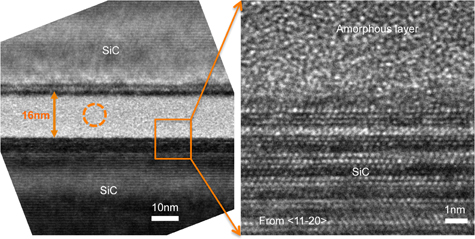
Fig. 6. HR-TEM Cross-sectional image of the SiC–SiC bonding interface without high temperature annealing.
Download figure:
Standard image High-resolution imageThe intermediate layer in Fig. 6 (circle area) was analyzed by the EDX point analysis. From the result shown in Fig. 7, it can be known that the intermediate amorphous layer contains Si, Fe, O, C, Ar, and Cr. The peaks of Cu in Fig. 7 should be from copper mesh, which was the sample holder used in TEM experiment. The Fe should be from the deposition of nano Fe adhesion layer. The C and Cr should be coming from the stainless steel ion source together with the Fe. The origin of Ar is most likely the remainder of the Ar ion beam used for activation. In addition, the nano Fe adhesion layer at the interface between the bulk SiC and the intermediate layer disappeared. It is assumed that the nano Fe adhesion layer has already diffused.

Fig. 7. EDX point analysis result of the circle area in Fig. 6.
Download figure:
Standard image High-resolution imageAfter annealing at 1273 K in vacuum for 1 h, the bonding strength of SiC wafers was also inspected. Since the samples were not enough, only two samples were used in the tensile strength test. Their tensile strengths are 32.8 and 32.7 MPa, respectively. This means the bonding strength between SiC wafers is still very higher after annealing.
Figure 8 shows a HR-TEM cross-sectional image of the SiC–SiC bonding interface after annealing at 1273 K for 1 h in vacuum. It can be seen that the thickness of the intermediate layer at the interface was reduced from ∼16 to ∼8 nm. The intermediate layer was still amorphous and there was no specific layer observed between the amorphous intermediate layer and SiC. The EDX point analysis results of the intermediate layer (circle 1 in Fig. 8) and SiC wafer (circle 2 in Fig. 8) were shown in Figs. 9(a) and 9(b). In the intermediate layer, the disappearance of Fe, Cr, Ar was revealed by the EDX analysis. In the SiC wafer side, only the C and Si, which are the composition of SiC, were detected.

Fig. 8. HR-TEM Cross-sectional image of the SiC–SiC bonding interface after annealing at 1273 K.
Download figure:
Standard image High-resolution image
Download figure:
Standard image High-resolution image
Fig. 9. EDX point analysis results of the intermediate layer (circle 1 in Fig. 8) and SiC wafer (circle 2 in Fig. 8).
Download figure:
Standard image High-resolution imageThe results of EDX line scanning analysis across the interface before and after annealing were shown in Figs. 10(a) and 10(b). From Fig. 10(a), it can be seen that the composition of the intermediate layer before annealing is mainly Si, Fe, and C. Only little Cr, Ar, and O exist. In addition, the Fe concentration profile does not have some remarkable peaks at the positions of the deposition of Fe layers. After annealing, only Si, C, and O were detected in the intermediate layer, as shown in Fig. 10(b). Corresponding to the intermediate layer, each profile of Si, C, and O has a composition change after annealing. For C, its mass ratio in the intermediate layer is much higher than that in SiC. For Si, it is the exactly opposite. Moreover, the mass ratio of O in the intermediate layer is considered to be constant.

Download figure:
Standard image High-resolution image
Fig. 10. EDX line scanning analysis of the interface before (a) and after (b) annealing, the inset in (a) shows the enlarged view of C, O, Ar, Cr, and Fe profiles in (a) from position 15 nm to position 55 nm.
Download figure:
Standard image High-resolution image
3.2. Discussion
3-in. 4H-SiC wafer bonding has been achieved by the modified SAB method at room temperature under 5 kN force for 300 s without any chemical-clean treatment and high temperature annealing. The bonding tensile strength between SiC wafers is greater than 32 MPa, and only a small peripheral region and few voids were un-bonded, which may be caused by the absence of close contact along the beveled wafer edges and the contamination from the environment during wafer transfer after surface activation. These un-bonded regions can be reduced by higher bonding pressure and cleaner environment.
During the analysis of the cross-section of the bonded wafer without high temperature annealing, an amorphous intermediate layer including Si, Fe, Cr, C, Ar, and O was found at the interface. No Fe layer was observed, which means that Fe–Si inter-diffusion have already occurred before annealing and also agrees with the gently changed Fe concentration profile.
Although there seems to be no affect on the bonding strength after annealing at 1273 K in vacuum for 1 h, the thickness of the amorphous intermediate layer at the interface was reduced to half, and while the amount of C and O increased, metal elements (Fe, Cr) and Ar disappeared. The reduction of thickness may be caused by the densification of the intermediate layer and the out-diffusion of some elements. As the disappeared elements were not detected in the SiC wafer side during the EDX analyses, it is assumed that Ar and the metal elements (Fe, Cr) diffused out via the interface and O diffused into the intermediate layer from the environment, and the intermediate layer might be oxidized. In addition, Kaplan et al. had reported that the thin Fe film (∼3 nm) could react with SiC substrate at 673 K to form Fe silicide, and after annealing at 723 K for 90 min, some graphite will be formed at the Fe surface because of the C freed from SiC diffusing to the surface.30) In this case (∼1 nm Fe), it is also possible that some reactions between SiC and Fe happened at the interface to form Fe silicide and graphite at the interface. Then the Fe in the silicide will diffuse at high temperatures like 1273 K, while the formed graphite can diffuse into the intermediate layer. This explanation is also reasonable for the increase of C elements in the intermediate layer after annealing.
4. Conclusions
SiC–SiC wafer bonding at room temperature was accomplished by the modified SAB method. Although without high temperature annealing, almost the entire wafer was bonded, and has a bonding tensile strength greater than 32 MPa. An amorphous intermediate layer was found at the interfaces before and after annealing. While no affect on the bonding strength, the high temperature annealing will cause the thickness reduction of the amorphous layer and the out-diffusion of some elements. Some reactions between the Fe layer and SiC wafer may be also caused by the annealing.
Acknowledgments
This research was partially supported by a Grant-in-Aid for Scientific Research (A), 2011, 23246125 from the Ministry of Education, Culture, Sports, Science and Technology.