

Abstract
The exceptionally high thermal conductivity of polycrystalline diamond (>2000 W m−1 K−1) makes it a very attractive material for optimizing the thermal management of high-power devices. In this paper, the thermal conductivity of a diamond sample capturing grain size evolution from nucleation towards the growth surface is studied using an optimized 3ω technique. The thermal conductivity is found to decrease with decreasing grain size, which is in good agreement with theory. These results clearly reveal the minimum film thickness and polishing thickness from nucleation needed to achieve single-crystal diamond performance, and thus enable production of an optimal polycrystalline diamond for heat-spreading applications.
Export citation and abstract BibTeX RIS
Polycrystalline diamond (PCD) components have been gaining popularity in recent years in industry and research as a result of the unparalleled properties of diamonds, such as high hardness, transparency, and high thermal conductivity.1) The growing range of applications includes thermal management (e.g., heat spreaders) for high-power electronics2) and optics for X-ray lasers, high-power lasers, and gyrotrons.3–5) Polycrystalline diamond is typically grown via chemical vapor deposition (CVD); the size and shape of grains, the concentration of defects, the quality of grain boundaries, etc. are rather sensitive to the chemistry used in the growth reactor.6–8) These factors determine the thermal conductivity of polycrystalline diamond, which ranges from a few watts per meter kelvin up to 2500 W m−1 K−1.9) Hence, to optimize the thermal performance of CVD diamond components, a thorough understanding of the mechanisms affecting their thermal conductivity is essential.
CVD-PCD is a complex material, exhibiting a columnar grain structure with grain sizes expanding through several orders of magnitude, increasing from the nucleation layer at the nanometer scale and through the material to the micrometer scale [see Figs. 1(a) and 1(b)]. This gradient in the grain size strongly affects phonon transport in the diamond; for instance, it is known that the thermal conductivity of the first microns of CVD-PCD is 10–20 times lower than the bulk values.9) Thus, to maximize the spreading of heat in the PCD film, the diamond should be grown up to some thickness at which the grains are sufficiently large to minimize their effect on phonon flow. Furthermore, the nucleation face should be polished to remove the small grain region, which reduces the heat-spreading properties of the film. To optimize this process, it is necessary to correlate the local thermal conductivity with the grain structure of the sample, which is typically circumvented by measuring samples of different thicknesses.10) However, there are limitations to the accuracy as the measurements are not all performed on the same sample. Therefore, accurate local measurements are required to adequately describe and predict the PCD thermal properties.
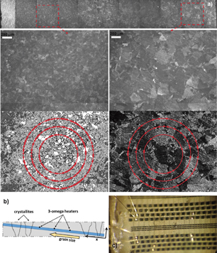
Fig. 1. (a) Optical micrographs showing the crystalline structure of and the grain size gradient in an oblique-cut diamond wafer. The local average grain size was determined by digitally enhancing the micrographs and counting the grain boundaries (marked by dots) intersecting a pattern consisting of three concentric circles, i.e., via the Abrams method,20) as illustrated. (b) A schematic showing the structure of a 290-µm-thick sample polished at 5.9° from a diamond slab. (c) A 3ω heater set covering the whole sample, showing one heater wire-bonded for measurement.
Download figure:
Standard image High-resolution imageMeasuring the thermal conductivity of diamond and other materials with high thermal conductivity to high accuracy generally poses significant challenges for measurement instrumentation. Laser flash and hot bar techniques have been adapted for this purpose and enable measurement accuracies better than 10%.11–13) However, these techniques measure the average thermal conductivity over large sample volumes in which the effect of the local grain structure is lost.
In this letter, we present the local, grain size-dependent thermal conductivity along the growth direction of a specially designed diamond sample with high accuracy. This allows in determining the effect of grain size on the thermal conductivity of PCD, revealing the minimum PCD thickness and polishing thickness needed to obtain similar heat-spreading performance to the more expensive and typically only 5–10 mm in size single-crystal diamond. For this purpose, the 3ω technique, which was originally designed for materials with lower thermal conductivity, is extended from the frequency range that is typically used14) to the higher frequencies needed for high thermal conductivity materials.
To capture the effect of grain size on the heat spreading properties of diamond films, a unique diamond sample with a thickness of 290 µm and lateral dimensions of 20 mm by 20 mm was prepared by polishing both sides of a 2-mm-thick CVD diamond slab at an angle of 5.9°, as shown in Fig. 1(b). The resultant oblique-cut wafer exhibits a gradient in grain size in the lateral direction (x), while the grain size is constant in the other lateral direction (y) [Fig. 1(a)]. The CVD diamond was grown following a commercial process recipe, which yields high-quality diamonds exhibiting average bulk thermal conductivity values above 2000 W m−1 K−1 for sample thicknesses above 600 µm.15) The oblique-cut wafer was oxygen-terminated through ozone treatment, and a dense grid of 3ω heaters was deposited via photolithography so that the heaters were perpendicular to the direction of the grain size gradient. The distance between the nearest heaters was 60 µm [Fig. 1(c)]. The heaters consisted of a 50 nm Ti adhesion layer and a 150 nm Pd layer with a width of 10 µm and an overall length of 1235 µm. This dense set allowed the thermal conductivity of the sample to be probed with high spatial resolution, and in turn the dependence of the thermal conductivity on the grain size to be extracted with high accuracy. Since the measurements were performed on a single sample, this ensured the results were not affected by sample-to-sample fluctuations that can occur when multiple samples are grown in a reactor. The heaters were wire-bonded and the sample was placed in a Linkam THMS600 thermal stage for measurement in a temperature-controlled environment.
The 3ω method applies a sinusoidal voltage of angular frequency ω to a metal line heater deposited on a sample, which gives rise to a temperature oscillation (ΔT) of angular frequency 2ω in the heater. This carries information about the thermal conductivity of the sample and causes a 3ω frequency component (V3ω) to emerge in the voltage drop along the line heater. The frequency-dependent ΔT(2ω) in the heater can be derived from the measured V3ω as:
where V0 is the ω component of the voltage drop along the heater and β is the temperature-resistance coefficient of the heaters, which was calibrated separately for each measured heater.
The ΔT(2ω) generated in an infinitely long heater with half-width b, located on the surface of a sample of infinite thickness with thermal conductivity κ, and operated at RMS power prms is given by14)

where
ω is the angular frequency, δ is the thermal penetration depth, cp is the specific heat capacity, and ρ is the density of the sample. From Eq. (1), it is clear that ΔT(2ω) is inversely proportional to the thermal conductivity and that it decreases monotonically with ω, vanishing in the high-frequency limit. When δ(ω) is in the range d ≫ δ ≫ b, ΔT(2ω) can be approximated with a linear function of ln ω:

where d is the thickness of the sample and ξ is a constant. Hence, in this frequency regime, the thermal conductivity can be extracted with high accuracy via a simple linear fitting of the measured ΔT vs ln ω; this is the so-called slope method.14)
In most reported studies using the 3ω method, the excitation frequency range does not exceed a few kilohertz. However, when the heat wave penetration depth is comparable to the thickness of the sample, i.e., the excitation frequency is lower than a critical value, the real temperature oscillation deviates from the one predicted by Eq. (4), and the accuracy of the thermal conductivity measurement is reduced. It is worth noting that the thermal penetration depth is proportional to the square root of the ratio of the thermal conductivity and the frequency as shown by Eq. (3). Therefore, Eq. (4) can be applied only to samples well over 250 µm thick in the typically used frequency range for good quality diamond. Hence, higher frequencies are required for diamond; herein, the 20–100 kHz range was used, corresponding to a probed depth of ∼150 µm. The combination of high frequency and high thermal conductivity results in a very low signal-to-carrier ratio, which is two orders of magnitude lower than it is for typically measured 3ω signals. This can cause significant measurement issues due to harmonic distortion of the electronics.16)
In order for this technique to be applicable in this low signal-to-carrier ratio scenario, the harmonic distortion was minimized. This was accomplished by using a signal generator with low output distortion to provide a driving signal and a differential input stage with a high common-mode rejection ratio and low input distortion for subtracting signals from the heater and the reference resistor (inset of Fig. 2). A Zürich Instruments HFLI lock-in amplifier was used for generating the driving signal and subtraction, and for detecting the 3ω signal. To achieve a high common-mode cancellation ratio, and to eliminate additional distortion produced by the differential amplifiers present in traditional 3ω setups, a highly tunable Wheatstone bridge, consisting of only passive elements, was chosen over the differential amplifier configuration (inset of Fig. 2).17) Resistors with a low thermal coefficient of resistance (±15 ppm/K) were chosen and the net resistance of the Wheatstone bridge was matched to the 50 Ω output impedance of the lock-in amplifier. The resistances of the arms of the Wheatstone bridge were equal, to minimize any phase differences due to the input capacitance of the lock-in. The ratio Rh/R1 was chosen to be ∼ , hence most of the power was dissipated in the heater. The resistor R2, with resistance close to that of the 3ω heater, was connected in series with a 20-turn trimmer resistor (Rv), which enabled the fine balancing of the bridge, and hence ensured the high common mode cancellation ratio needed for measuring the diamond sample. The change in ΔT over the scanned frequency range was ∼5–10 m·K and it exhibited a highly linear behavior in the frequency range used, as shown in Fig. 2. The uncertainty of the local thermal conductivity values determined via this method was less than 8%, with the error arising mainly from residual harmonic distortion of the electronics.

Fig. 2. Plots of the typical ratio of temperature change (ΔT) to electrical power (P) versus the logarithm of angular frequency (ln ω), measured on the diamond sample; the gradient is inversely proportional to the thermal conductivity. Red triangles correspond to the region with larger grains (right axis). The inset shows a schematic of the Wheatstone bridge used for obtaining the 3ω signal.
Download figure:
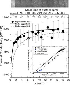
Standard image High-resolution imageThe thermal conductivities measured along the sample are shown in Fig. 3. There is an apparent decrease in the thermal conductivity from 2200 W m−1 K−1, i.e., single-crystal values, in the region with large grain size to around 1900 W m−1 K−1 in the region with smaller grains. The maximum values are thus close to what has been reported for II-a single-crystal diamond.18)
Fig. 3. Measured thermal conductivity (solid circles) as a function of the lateral coordinate in the oblique-cut diamond wafer. The origin of the x-axis corresponds to the low-grain-size edge of the wafer; see the micrograph aligned with the axis. Solid and dashed lines represent the thermal conductivity values predicted by a phonon scattering model using the estimated upper and lower limits of the thickness vs surface grain size, shown in the inset.9,10,21)
Download figure:
Standard image High-resolution image
In order to further understand the observed thermal conductivity dependence measured along the diamond wafer, we analyzed the thermal conductivity of this sample by means of the phonon scattering model described in Ref. 9. This model can distinguish between the contributions from different scattering mechanisms. The thermal conductivity is defined as
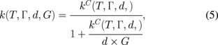
where Γ is a parameter characterizing the quality of the lattice, which, given the high thermal conductivity, can be assumed here to be equal to that of natural diamond, as fully described by Morelli et al.19) This also means that the concentrations of dislocations, extended defects, and vacancies can be assumed to be negligible and the dominant scattering mechanisms are isotope scattering and grain boundary scattering. Next, G is the thermal conductance between grains, taken to be the highest value reported in Ref. 9 (3 GW/m2·K). Finally, kC is the intra-grain lattice thermal conductivity; calculated through the Callaway–Holland model detailed in Ref. 9, which includes the effect of grain boundary scattering.
In principle, this phonon scattering mechanism is frequency dependent, since some of the phonons are specularly scattered at the grain boundaries, depending on their frequency. However, this effect is only noticeable in diamond well below room temperature, and thus it is possible to assume frequency-independent grain boundary scattering in the investigated temperature range without loss of generality.20) Therefore, under this approach, the phonon grain boundary scattering rate can be defined as

where vi is the sound velocity of each phonon branch and LGS is a measure of the average mean free path between scattering events by grain boundaries. Given the columnar structure of this diamond, this distance can be characterized by the average lateral distance between grain boundaries, and thus by the lateral average grain size, as described in Ref. 9.
Therefore, in this simplified formalism, there is no free parameter, and only the average grain size (d) and its evolution with the thickness — which can be obtained from the grain size at the surface — is needed for this model to compare to the measured experimental data. Based on the optical micrographs, the local average grain sizes over parts of the wafer were determined using the Abrams method.21) After digital enhancement, a pattern consisting of three concentric circles of adequate radii was drawn on the images and the number of grain boundaries intersecting the pattern was counted [Fig. 1(a)], from which the average grain size at the surface was calculated. However, at the low grain size side of the sample, it was not possible to obtain a good quality micrograph, owing to the roughness of the back side of the sample and the low grain size; hence, the grain size measurement resulted in values with high uncertainty, as shown by the error bars in Fig. 3 inset. To circumvent this limitation, i.e., to obtain a more accurate grain size distribution over the whole sample, our grain size data were combined with the data reported in the literature for grain size at the surface vs the diamond thickness (Fig. 3, inset).9,19,22)
A strong correlation of over three orders of magnitude between the grain size and the thickness from near the nucleation region was observed, which also describes the evolution of average lateral grain size with thickness. However, since the local grain size follows a rather broad distribution in our sample, as shown in the inset of Fig. 3, we determined upper and lower limits for the grain size evolution, rather than a single average trend. The predicted dependence of the thermal conductivity along the sample as a function of grain size is given in Fig. 3. Excellent agreement with the experimental data is observed, regardless of whether the upper or lower limits of the grain size estimation are used in the thermal conductivity model. The results shown in Fig. 3 accurately show the impact of grain size at room temperature and above in samples with thickness of ≥100 µm, which are commonly used for heat sinking applications. In addition, it is clear from Fig. 3 that, to achieve thermal conductivity in single-crystal diamond (>20 W cm−1 K−1), the diamond film should be thicker than 500 µm (corresponding to ∼5 mm in the lateral coordinate x) and therefore at least >220 µm should be polished from the nucleation face for this particular material. Furthermore, the model enables extrapolation of the thermal conductivity below 100 µm, showing that for a diamond film with a thickness of only 50 µm (non-polished) the thermal conductivity drops to 13–16 W cm−1 K−1, i.e., 60% of the single-crystal thermal conductivity.
It is worth noting that in diamond at room temperature almost all the heat is carried by phonons with a mean free path smaller than 10 µm.23) As a consequence, the thermal conductivity reduction at room temperature and above only becomes significant when the grain size is reduced to below ∼20 µm. This threshold however shifts to lower grain sizes at high temperatures as intra-grain scattering processes become dominant. On the other hand, the strength of grain boundary scattering would increase even for grain sizes well above 20 µm at cryogenic temperatures, and hence the grain-size dependence of the thermal conductivity would be significantly enhanced.
In conclusion, we have shown the effect of grain size on thermal conductivity of CVD diamond films typically used as heat-spreaders by using an optimized low-noise 3ω technique, which is also suitable for measuring other materials with high thermal conductivity. The experimental data compares well with a theoretical model describing phonon scattering in CVD diamond, which also enabled extrapolation of thermal conductivity below 100 µm in thickness, showing that for 50-mm-thick PCD films, the thermal conductivity is 60% of that observed in single crystal-diamond. We have also shown that, to achieve single-crystal performance, the PCD film should be thicker than 500 µm and that ∼200 µm should be removed from the nucleation face. These findings are important for the optimization of the growth, fabrication, and thermal properties of heat spreaders and other CVD diamond components used in high-power applications.
Acknowledgments
We acknowledge the financial support from the Engineering and Physical Sciences Research Council (EPSRC). We thank our colleagues at the University of Bristol, namely James W. Pomeroy and David Cussans for their advice regarding the 3ω electronics and Maire J. Power for proofreading of the manuscript. This work is in part supported by DARPA Contract No. FA8650-15-C-7517, monitored by Dr. Avram Bar Cohen and Dr. John Blevins and supported by Dr. Joseph Maurer and Dr. Abirami Sivananthan. Any opinions, findings, and conclusions or recommendations expressed in this material are those of the authors and do not necessarily reflect the views of DARPA.