

Abstract
The directional atomic layer etching (ALE) of GaN and AlGaN has been developed. The GaN ALE process consists of cyclic Cl2 plasma chemisorption and Ar ion removal. The etch per cycle (EPC) was 0.4 nm within the self-limiting regime, which is 50 to 100 V. The root-mean-square surface roughness RRMS was 0.6 nm, which was improved from an initial roughness of 0.8 nm. For AlGaN ALE, BCl3 was added to the chlorine step to obtain a smooth surface with RRMS of 0.3 nm and stoichiometry similar to the initial sample. The ultra smooth surface obtained by etching is promising for use in next-generation power devices.
Export citation and abstract BibTeX RIS
1. Introduction
As next-generation power devices, wide-band-gap semiconductors are being developed. GaN is a promising candidate because of its excellent high-power and high-speed performance. The high electron mobility of GaN devices is realized by an AlGaN/GaN heterojunction, which induces two-dimensional electron gas (2DEG). However, owing to the structure, electrons always exist under the gate electrode unless it is negatively biased (normally on). For commercial applications, the normally on operation is not preferable. To make the device normally off, several structural approaches have been proposed such as a recessed gate1) and p-GaN gate.2) Since feature size fidelity is important to make the devices operate as designed, they are expected to be fabricated by plasma dry etching. Because of the chemically inert nature of GaN, simple wet etching using an acid or base is difficult,3) and the other conventional technique of ion milling causes serious damage.4) Plasma dry etching of GaN using a number of chemistries, mostly halogens or methane,4–13) has been studied, mainly for the purpose of obtaining a high etching rate and anisotropy. However, exposure to plasma also induces various types of damage,14–23) which cause the degradation of device performance. Although several post-treatments have been proposed,24–28) a damage-free etching process is desirable and atomic layer etching (ALE) is one of the promising candidates.
ALE is expected to achieve atomic-scale etching control for nanoscale device fabrication.29,30) Ultra thin layers of the material are removed by a multi step cycling process, which consists of self-limiting surface modification and removal. Several approaches can be considered for surface modification such as chemisorption, deposition, converting the top layer, and extraction. For removal, the use of thermal, chemical and bombarding energy can be considered. With the exception of removal by bombardment, process characteristics will be isotropic. ALE has been studied as a derivative of atomic layer deposition (ALD) and recently highlighted as a method that can break through the limitations of continuous etching processes. Whereas all species interact simultaneously in continuous processes, in the ALE process, surface modification and removal are functionally separated, which enables more precise process control and less ion-induced damage. High selectivity and better uniformity across the wafer are also achievable.29) Moreover, since it is necessary to maintain post etching stoichiometry, ALE has been investigated for various compound semiconductors.30) In previous reports of GaN/AlGaN ALE, the surface was first oxidized with either O2 plasma31,32) or H2O2 solution33) and then removed with either HCl acid solution31,33) or BCl3 plasma.32)
In our study, a directional type of ALE is used to examine GaN and AlGaN etching for the fabrication of p-GaN gate-type devices. In our ALE approach, the surface is modified using chlorination instead of oxidation. The removal step uses Ar ion bombardment, which enables directionality in a patterned feature.
2. Experimental methods
All experiments were performed in a commercially established transformer coupled plasma (TCP) etching system (Kiyo® F Series conductor etch system) equipped with advanced mixed mode pulsing (AMMP). AMMP provides fast, repeatable, and reliable power/gas switching, which ensures the sufficient robustness of the process for production. GaN and AlGaN blanket samples were used to examine the amount of etching and surface roughness. Each sample was cleaned in advance by HF to remove native oxide on the surface and N2 dried. The ALE process consisted of cyclic plasma chlorination followed by Ar ion bombardment with applied bias voltages ranging from 20 to 150 V. The pressure in the non-biased chlorination step was 60 mT and the duration was 2.5 s. The pressure applied for Ar removal was 5 mT and the duration was 5.0 s. These step times were determined in preliminary studies to be sufficient lengths for each reaction to be fully completed under the conditions. Between these steps, a non-plasma purge step was inserted to minimize interactions. For comparison with the ALE process, a continuous process was also analyzed. The continuous process used Cl2/Ar chemistry simultaneously and was operated at 50 V bias.
The etch per cycle (EPC) of the ALE process was calculated by dividing the total amount etched by the number of cycles. The etch depth was measured by ellipsometry (Woollam M-2000) and transmission electron microscopy (TEM; FEI Tecnai TF-30). Atomic force microscopy (AFM; Veeco Vx310) was used to measure the surface roughness for plasma damage estimation. The initial surface roughnesses RRMS were 0.8 and 0.4 nm for GaN and AlGaN, respectively. The stoichiometry of the AlGaN surface was determined by X-ray photoelectron spectroscopy (XPS; Thermo Scientific K-Alpha with 0.1–0.2% detection limits) since the composition ratio will affect device characteristics.
3. Results and discussion
Figure 1 shows the EPC of GaN as a function of RF bias voltage. Three different process regimes are visible, consistent with previous studies of silicon.34) In regime I (0–50 V bias) and regime III (>100 V bias), the EPC increased with the bias voltage, while in regime II (50 to 100 V), the EPC is almost constant. From our prediction of GaN ALE mechanism, which is surface modification by Cl2 plasma and the desorption of volatile by-products such as GaCl3 and N2 formed by the energy delivered from Ar ion bombardment, this behavior can be explained as follows. In regime I, the ion energy is insufficient to remove plasma-modified compounds completely. In regime III pure sputter etching occurs, where the ion energy exceeds the physical sputtering threshold. The boundary, 100 V is in good agreement with the reported threshold energy of approximately 100 eV for GaN obtained by experiment35) and molecular dynamics simulation.36) In regime II, a self-limited EPC was observed and the regime can be considered as the ALE window30) for this system. The EPC in this regime of 0.4 nm corresponds to one or two layers of GaN crystal. Since the ion energy is below the sputtering threshold, it suggests that only a few layers of GaN are chemisorbed by the preceding chlorination step. As compared with the Si ALE window of 40–60 eV,34) the GaN window of 50–100 eV is notably shifted to higher energies. According to basic sputtering theory, the sputter threshold, represented by the upper limit of the ALE window, scales with the surface binding energy. For example, the Si surface binding energy is 4.7 eV,37) compared with the stronger GaN surface binding energy of 8.6 eV.38) This widens the overall process window as observed, and is consistent with trends recently reported for other materials.39)

Fig. 1. EPC of GaN as a function of bias voltage for a fixed Ar step time of 5 s.
Download figure:
Standard image High-resolution imageIn the ALE window (80 V), etching synergy was confirmed by comparison between the EPC of ALE (full cycle), chlorination only, and Ar sputtering only (Fig. 2). Each step was executed individually for 90 cycles. The EPC of chlorination was negligible and Ar sputter was 0.05 nm, contributing only ∼10–15% of the ALE process. The result showed that the basic concept of reactive ion etching, synergistic effect of neutrals and ion bombardment40) was confirmed, and was completely separated in this process.
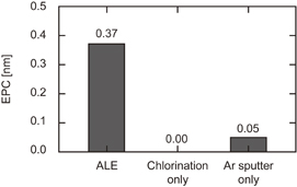
Fig. 2. Results of EPC synergy test at 80 V bias.
Download figure:
Standard image High-resolution imageThe RRMS GaN surface roughness after ALE of 0.6 nm was an order of magnitude less than that of 4.0 nm after the continuous plasma process with the same etched depth. The TEM image in Fig. 3(a) suggests that crystal structures were kept intact beneath the etch front of ALE. Although we have to take into account the effect of UV light irradiation,21,22) from the surface morphology point of view, this smoothness is attributed to the layer-by-layer self-limiting nature of ALE and is a characteristic advantage over the conventional continuous plasma process. Moreover, the injection of reactive ions such as Cl+ or Cl2+ is minimized in ALE, which may prevent the increase in surface roughness seen in the continuous process.
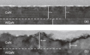
Fig. 3. Cross-sectional TEM images of GaN processed with (a) ALE and (b) continuous plasma process.
Download figure:
Standard image High-resolution imageFor AlGaN ALE, we first employed the same ALE process as that used as for GaN, expecting that the same etching mechanism would form volatile metal chlorides. However, in contrast to GaN, measurable surface roughness was observed with the Cl2-only ALE approach. As shown in Figs. 4(a) and 4(b), RRMS was 1.8 nm as compared with 0.4 nm for the pre-etch sample. XPS measurements detected higher amount of O on the roughened surface [Fig. 5(b)], suggesting the formation of non-volatile AlO, which act as a micromask and roughens the surface. Oxygen is assumed to be provided from the ceramic parts inside the chamber. Therefore, BCl3 was added to the chlorination step to prevent oxidization by scavenging BClO.41–43) With BCl3/Cl2 ALE, the stoichiometry post-ALE became similar to that of the initial pre-etch sample (Fig. 5). As further evidence that ALE was working properly, RRMS recovered to 0.3 nm [Fig. 4(c)].
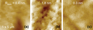
Fig. 4. AFM images of AlGaN surface. (a) Initial, (b) Cl2 ALE, and (c) BCl3/Cl2 ALE.
Download figure:
Standard image High-resolution image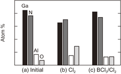
Fig. 5. Results of XPS analysis of AlGaN surface. (a) Initial, (b) Cl2 ALE, and (c) BCl3/Cl2 ALE.
Download figure:
Standard image High-resolution image
4. Conclusions
A GaN and AlGaN etching process to obtain an ultra smooth surface was realized by ALE. The ALE window was observed for GaN by cyclic Cl2 plasma modification and Ar ion removal process. In the ALE window of 50–100 V, the EPC was around 0.4 nm. For the AlGaN process, BCl3 was added to scavenge oxidized materials on the etch front. The post-ALE RRMS obtained was 0.3 nm, and the stoichiometry was similar to that of the initial pre-etch sample. Further work is required to confirm the correspondence between these characteristics and actual device electrical properties.