
Abstract
We report on InGaN edge emitting laser diodes with a top metal electrode located beside the laser ridge. Current spreading over the ridge is achieved via a highly doped n+-type GaN layer deposited on top of the structure. The low sheet resistance of the n+-GaN layer ensures excellent lateral current spreading, while carrier injection is confined all along the ridge thanks to current tunneling at the interface between the n+-GaN top layer and the p++-GaN layer. Continuous-wave lasing at 400 nm with an output power of 100 mW is demonstrated on uncoated facet devices with a threshold current density of 2.4 kA·cm−2.
Export citation and abstract BibTeX RIS

Content from this work may be used under the terms of the Creative Commons Attribution 4.0 license. Any further distribution of this work must maintain attribution to the author(s) and the title of the work, journal citation and DOI.
The pioneering work performed on III–nitride semiconductors, particularly on Mg doping of GaN by Amano et al.1) and Nakamura et al.2) at the end of the last century has resulted in the development of high-efficiency light-emitting diodes (LEDs) and laser diodes (LDs) in the near-UV and visible spectral range. These devices are nowadays widely used for solid-state lighting and high-density data storage. Despite the huge progress in device performance, p-type III–nitride layers are still a bottleneck for future GaN optoelectronics because of the fact that the Mg acceptor species exhibits a high activation energy,3,4) the holes possess a large effective mass, and the contacts require metals with high work functions. Consequently, the specific contact resistance on p-GaN is rather high, typically in the 10−4 Ω·cm2 range, and the layer resistivity is limited to 0.2 Ω·cm.5) Such modest electrical properties are likely detrimental when dealing with high-power lasers. In addition, the tensile strain that builds up in the AlGaN alloy when deposited on GaN imposes laser structures featuring low-Al-content AlGaN cladding layers. As a consequence, the refractive index contrast between the waveguide and the cladding is marginal, which makes mandatory the use of thick cladding layers, and thus a large series resistance, especially from the p-side. The cladding issue in GaN laser technology becomes even more critical when pushing the wavelength emission toward green, since the refractive index contrast between GaN and AlGaN decreases in this spectral range. This may induce additional optical losses as a result of the optical mode overlap with the upper metallic contact. These material constraints make the realization of efficient LDs very challenging in both the green spectral range6,7) and below 360 nm.8,9) Thus, alternative strategies to the standard AlGaN cladding layers have been proposed but have yielded no clear benefit so far.10–12) One promising solution is to reduce the thickness of the AlGaN top cladding while completing the top laser structure with a transparent conductive contact, possibly with a low refractive index. Such a laser design was successfully demonstrated using indium tin oxide.13)
In this paper, we report on InGaN LDs with transparent n+-GaN top layers and with the top metallic contact beside the ridge. Current spreading from the metallic contact to the ridge is ensured by the n+-GaN layer, while the carrier injection on top of the ridge is achieved via a tunnel junction.14–16) This geometry relaxes the constraint of the low modal field at the ridge surface and allows for a device with a very thin AlGaN top cladding layer. In this work, we demonstrate InGaN LDs with only a 200 nm p-type Al0.06Ga0.94N cladding in continuous wave (cw) operation and with a threshold current density of 2.4 kA·cm−2.
The laser structure was grown by combining metalorganic vapor phase epitaxy (MOVPE) and molecular beam epitaxy (MBE). In order to highlight the potential of a lateral top contact (LTC) electrode set aside from the ridge, we designed a LD with a reduced Al0.06Ga0.94N:Mg top cladding thickness of 200 nm compared with standard reference devices featuring 500-nm-thick top claddings. The laser structure is completed with a 50-nm-thick p++-GaN layer and terminated by 150 nm of n+-GaN serving as a contact and current-spreading layer. A schematic representation of the final device architecture is shown in Fig. 1. The optical modes in the reference and LTC lasers were simulated using a commercial three-dimensional finite difference eigenmode solver.17) Plasmonic effects that could arise from the high n-type doping concentrations were not considered in the simulation.18) The thicknesses of the p-AlGaN, p++-GaN, and n+-GaN top layers were chosen to keep the waveguide thickness and the active region separation from the bottom cladding the same with respect to reference LD structures. It is worth noting that the reduced thickness of the top cladding with respect to reference structures allowed the bottom AlGaN cladding thickness to be increased by 100 nm in order to decrease the leakage of the optical mode into the substrate.
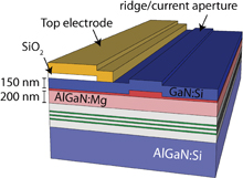
Fig. 1. Schematic view of the LTC device architecture (blue: n-type layers; red: p-type layers).
Download figure:
Standard image High-resolution imageThe main parameters considered in this study were the mode overlap with the active region (ΓQWs), the p-type cladding layer (ΓCL), and the p++ layer ( ) for both LTC-LDs and standard LDs. Results from the simulation (Table I) show that the overlap with the active region remains essentially unchanged, while the overlaps with the top cladding layer and the p++ cap are slightly larger, as expected from the thinner AlGaN:Mg cladding. We therefore expect a slight increase in the internal losses owing to the higher overlap with the top cladding layer (ΓCL) and the heavily doped p-type cap (
 ).19,20) However, this drawback might be counterbalanced by the lack of absorption in the top contact electrode (no longer present at the ridge surface).
Table I. Modal overlaps among various regions of the standard LD and the LTC-LD (in %).
| Device | ΓQWs | ΓCL |  |
|---|---|---|---|
| Standard LD | 4.3 | 10.6 | 0.008 |
| LTC-LD | 4.1 | 12.0 | 1.5 |
The realization of the LTC-LDs with a targeted emission wavelength of 400 nm started with the MOVPE growth of the structure up to the GaN:Mg++ cap layer. Epitaxy was performed on a freestanding (FS) c-plane GaN substrate with a dislocation density in the 1 − 5 × 106 cm−2 range. Standard patterning technology was used to define the ridge and the current aperture: the p++-GaN cap layer was protected by a photoresist mask in the current aperture/ridge regions and was partially etched/passivated outside. The sample was then transferred into an MBE reactor for the deposition of 150 nm of highly doped n-type GaN, similarly to the method described in Refs. 21 and 22. High Si doping levels above 1 × 1020 cm−3 were used at the regrowth interface and at the contact surface to obtain efficient tunneling and low contact resistances, respectively. The doping level was lowered to the 1019 cm−3 range in the inner part of the layer to keep potential absorption losses at a minimum value. Note that a degradation of the surface morphology of the n+-type GaN layer was observed by reflection high-energy electron diffraction during the MBE growth, which could negatively impact the LD performance.
Following the MBE growth step, LD devices with a design suitable for the LTC were fabricated. A SiO2 isolation layer was deposited on the surface, except on the ridges and their close surroundings. Ti/Au metallization was used for both the lateral top contact on the n+-GaN spreading layer and for the bottom electrode. Cavities were formed by cleaving the laser bar and the facets were left uncoated.
The electrical characteristics of the n+-GaN spreading layers were studied by the transfer line method on specifically processed test structures. Sheet and specific contact resistances of 30 Ω/□ and <1 × 10⁻⁵ Ω·cm2, respectively, were systematically obtained. LED test structures were also fabricated in order to estimate the injection uniformity. The carrier spreading length (Ls) was estimated using the method described in Refs. 23 and 24. For a bias voltage of 5 V, Ls is on the order of 100 µm, which demonstrates the suitability of such layers for efficient current spreading. The injection homogeneity was further confirmed in the LTC-LDs through micro-electroluminescence (µ-EL) imaging performed on top of the ridge surface. Figure 2(a) shows a 40 × 40 µm2 µ-EL mapping. The emission intensity is quite homogeneous at the resolution scale (8 µm), as well as at a much larger scale under an optical microscope [Fig. 2(b)].
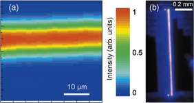
Fig. 2. (a) 40 × 40 µm2 µ-EL intensity mapping of an 8-µm-wide ridge, and (b) optical micrograph of a 1000 × 8 µm2 device electrically injected at 11 A/cm2.
Download figure:
Standard image High-resolution imageThe L–I–V characteristics of the LTC-LDs were finally recorded. The laser bars were mounted with indium on a copper plate as a heat sink, and lasing was successfully achieved under cw operation. Lasing was observed above a threshold current density (JTh) of 2.4 kA·cm−2 on 1000 × 8 µm2 devices with a slope efficiency of ∼0.4 W/A. The L–I–V characteristics are plotted in Fig. 3(a) along with the corresponding far-field pattern [Fig. 3(b)]. The L–I characteristics were also measured under pulsed operation (1% duty cycle; 1 µs pulse width) to investigate the role of heating effects, if any, on the LTC-LD performance. Both JTh and the slope efficiency remained unchanged with respect to those obtained from the cw measurements. The far-field comparison with a standard LD is shown in Fig. 4. The intensity dip observed in the far-field pattern of the reference laser [Fig. 4(a)] is absent in the case of the LTC-LDs [Fig. 4(b)]. This feature is a characteristic signature of parasitic mode leakage into the GaN substrate.7) This result is in good agreement with simulations (not shown here), and indicates an optical guided mode stretched toward the upper surface in the structure with an n+-GaN spreading layer.
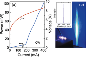
Fig. 3. (a) L–I–V characteristics of a 1000 × 8 µm2 uncoated device under cw operation, and (b) far-field pattern with corresponding lasing emission spectrum in inset.
Download figure:
Standard image High-resolution image
Fig. 4. Far-field patterns of (a) standard laser and (b) LTC-LD.
Download figure:
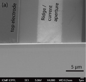
Standard image High-resolution imageWhen the L–I characteristics are compared with standard LDs measured under the same conditions, we observe an increase in the threshold currents by ∼20% and a decrease in the slope efficiency by ∼40%, which are likely due to several factors. As aforementioned, the n+-type GaN layers have a tendency to become rough during MBE growth. Scanning electron microscopy (SEM) was performed on the laser structures (Fig. 5). While the growth beside the ridge area produced a smooth n+-GaN surface, a pronounced surface roughening was observed on top of the current aperture [Fig. 5(b)]. Such three-dimensional growth is attributed to contamination at the regrowth interface induced by the photoresist mask used to create the current apertures/ridges. Such a surface roughness combined with the increased ΓCL and  may be responsible for an increase in the optical losses. In addition, absorption losses can also take place in heavily doped GaN layers. Experiments are currently under way to extract the actual absorption in n+-GaN layers as a function of the doping level.

Download figure:
Standard image High-resolution image
Fig. 5. (a) SEM image of an 8-µm-wide ridge laser. The top metal contact is 5 µm beside the ridge. (b) Magnified view of the surface of the n+-GaN layer grown on top of the ridge.
Download figure:
Standard image High-resolution image
The I–V characteristics of the LTC-LDs are affected by the presence of a reverse-biased TJ (n–p) at the top of the standard (p–n) device structure. This introduces an additional resistance, which is inversely proportional to the hole tunneling probability through the n–p interface, to the characteristics of the p–n junction. The voltage at the threshold (VTh) of the LTC-LDs is 3.5 V higher than that measured on reference LDs. Given the very low specific contact resistance of n+-GaN used in the LTC-LDs (measured by the transmission line method to be <1 × 10⁻⁵ Ω·cm2), we attribute the increase in VTh to the TJ. This increase may be due to the nonoptimized doping profile and/or to process-induced surface contamination prior to n+-GaN regrowth, as revealed by the poor surface morphology of the n+-GaN layer on top of the ridge. In this regard, an improvement of the I–V characteristics of the LTC-LDs is expected by implementing a careful surface cleaning procedure prior to the MBE growth and by increasing the doping levels at the interface.
In conclusion, we demonstrated InGaN lasers with a metal-free ridge using an n+-GaN top layer. Current spreading from the top metallic contact to the ridge is ensured by the n+-GaN layer, while the carrier injection is achieved via a tunnel junction. This geometry relaxes the constraint of low modal field at the ridge surface and allows for a device with only a 200 nm p-type AlGaN cladding layer. Those lasers work under cw operation and with a threshold current density of 2.4 kA·cm−2. The reduced thickness of the p-type cladding layers in combination with the highly conductive and transparent n-type spreading GaN layer could ultimately improve the performance of UV and high-power LDs, and give rise to new device concepts.
Acknowledgment
This work was supported by the CTI-KTI project "High power GaN-lasers for white light generation" 17519.1 PFEN-NM.