
Abstract
We investigated ultrafast photogenerated carrier dynamics on a semi-insulating GaAs surface using femtosecond time-resolved core-level photoelectron spectroscopy. We observed a transient change in the surface potential where the Ga-3d core-level peak instantaneously shifted by ∼350 meV toward a higher binding energy within 2 ps of a 100 fs laser irradiation. A comparison of the experimental results with numerical simulations based on a drift-diffusion model of a semi-insulating semiconductor revealed that the transient surface potential change was mainly due to the photo-Dember effect, whereby the large difference in the carrier diffusion between the electron and hole instantaneously induced a surface photovoltage.
Export citation and abstract BibTeX RIS
The dynamical behavior of non-equilibrium carrier transport in semiconductor surface regions has been investigated intensively from both scientific and technological viewpoints. This is because it is the key factor for aspects such as the performance, response speed, and conversion efficiency in various semiconductor applications, including photosensing, photovoltaics, photocatalysis, and photoemission.1–4) Terahertz radiation technology based on photo-excited semiconductor surfaces is described as an outstanding example. Various terahertz emission properties are closely related to non-equilibrium photogenerated free carrier transport.5,6) In addition, the recent emergence of a wide variety of two-dimensional (2D) materials and their heterostructures, which has opened the door for novel higher-speed or more efficient photonic devices, demands a better understanding of the dynamics of the photogenerated carrier transport in such 2D systems.7) Thus, the importance of the non-equilibrium carrier transport in the surface region has increased continuously as we have progressed from traditional semiconductors to 2D materials.
Previously, the dynamical behavior of the photogenerated free carriers was mainly investigated using time-resolved reflectivity techniques based on an ultrashort pulse laser.7,9) Time-resolved core-level photoelectron spectroscopy in the extreme ultraviolet region (TR-EUV-PES) based on a synchrotron radiation source has been used as a more direct approach than such optical measurements.10,11) Although synchrotron-based TR-EUV-PES can directly probe the surface potential change as a result of the carrier transport with sufficient surface sensitivity,12) its temporal resolution is limited to the sub-nanosecond to microsecond range. This is far slower than the fundamental time scale of the surface carrier processes, i.e., from femtosecond to picosecond.
Recent technological progress in high-order harmonic generation (HHG) has provided us an opportunity to improve the temporal resolution significantly down to the femtosecond level.13–15) Despite its technological potential, time-resolved core-level PES based on HHG has not yet been applied for the measurements of non-equilibrium carrier transport, except in a pioneering work.14) In that work, the technical usefulness of time-resolved core-level PES based on HHG was demonstrated, but the physics remain to be detailed.
Here, we report a study combining a femtosecond core-level PES experiment based on an HHG source and a numerical simulation using the drift-diffusion model for the ultrafast dynamics of photogenerated free carriers with near band-gap excitation on a semi-insulating GaAs surface. We showed that the transient Ga-3d peak shift of ∼350 meV observed in the experiment is caused by the photo-Dember effect, which induces an instantaneous spatial electron–hole separation due to the large difference in the carrier diffusion between the electron and hole, and the resultant photovoltage.
We performed time-resolved core-level PES experiments with the femtosecond TR-EUV-PES system that we developed by combining a 59th harmonic (92.5 eV) source and a time-of-flight (TOF) photoelectron energy analyzer. The basic design of the femtosecond TR-EUV-PES system is very similar to that described in our previous study; however, we significantly improved its temporal resolution to the 100 fs level from a few hundred picoseconds.16) The use of a 92.5 eV harmonic pulse as a PES probe made it possible to achieve the ultimate surface sensitivity on the scale of a few atomic layers. The temporal resolution of this system is limited by the pulse duration of the 59th harmonic, which was estimated as 100 to 200 fs in our previous pulse-duration measurements of high-order harmonics.17) The sample that we used in this experiment was a semi-insulating GaAs(001) substrate, which we annealed at 400 °C for 15 min in an ultrahigh vacuum after employing chemical etching to remove a native oxidation layer from the GaAs sample. All the pump and probe measurements were performed at room temperature.
Figure 1(a) shows a typical photoelectron spectrum of GaAs(001) measured with our PES system. This figure shows the valence bands and the core level peak of GaAs in the binding energy from 0 to 25 eV. In the pump and probe experiment, we specifically measured the change in the Ga-3d peak near 20 eV induced by the pump irradiation. Figure 1(b) shows a typical transient change in the Ga-3d peak at a delay time of 1 ps after the pump pulse irradiation. The spectrum clearly shows that the Ga-3d peak shifts by approximately 350 meV toward a higher binding energy compared with that of the reference sample. A similar transient core-level peak shift from 250 to 350 meV with a pulsed laser irradiation was observed in p-type GaAs in several previous studies.10,11,18) Because it is generally accepted that an energy shift of a core-level photoelectron peak directly reflects the surface potential, e.g., the band bending in semiconductors,12) the previous studies concluded that the transient core-level energy shift corresponds to a transient modification of the surface potential induced by the laser irradiation. Thus, the energy shift shown in Fig. 1(b) is likely to be related to be the transient modification of the surface potential, as discussed later. The time-delay variation of the Ga-3d peak with the pump pulse irradiation is mapped in Fig. 1(c). The peak rapidly shifts toward a higher binding energy within 2 ps. After that, the peak position remains almost unchanged for 15 ps despite showing a slight tendency to relax to its original position.
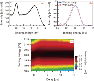
Fig. 1. Typical photoelectron spectrum of GaAs(001) over the entire energy region measured using our femtosecond core-level PES system (a). Spectra of the Ga-3d core-level peak obtained with (red) and without (blue) laser irradiation at a time delay of 1 ps (b). The fluence of the pump pulse was 0.1 mJ/cm2, which corresponds to 1 × 10⁹ W/cm2. Photo-induced transient change in the Ga-3d peak at various time delays (c). All the spectra were obtained from an accumulation of 18,000 laser shots.
Download figure:
Standard image High-resolution imageThe transient core-level peak shift of doped GaAs with laser irradiation was reported in several previous studies.11,18) With doped semiconductors, the origin of the surface potential change is generally explained by the effect of the "built-in" electric field on the photogenerated free carrier transport. In contrast to doped semiconductors, the "built-in" electric field is generally negligible in semi-insulating semiconductors because the band is almost flat, suggesting that the peak shift observed in our experiment is not attributed to the "built-in" electric-field effect.
With semi-insulating semiconductors, the most probable mechanism driving the change in the surface potential is the photo-Dember effect.8,19) The essence of the photo-Dember effect is the large difference between the diffusion of the electrons and that of the holes. In GaAs, the electrons have a far higher mobility than the holes. Because the diffusion coefficient is proportional to the mobility according to a generalized Einstein relation [Eq. (2)], the electrons diffuse considerably further away than the holes. The large difference in the diffusion drives the spatial separation of the photogenerated electrons and holes and results in the accumulation of more positive charges in the surface region compared with the bulk region. Subsequently, the resultant electric field induced by the charge separation modifies the surface potential. Therefore, in the absence of any other effect, the photo-Dember effect induces the change in the surface potential. This contrasts the mechanism in doped semiconductors, wherein an intense "built-in" electric field of several hundred kV/cm, which is generally produced by pre-existing band bending in the doped semiconductor surface region, drives the drift motion of the photogenerated electrons and holes in the opposite direction; then, the resultant spatial separation of the photogenerated electrons and holes modifies the surface potential.12,18)
To confirm the aforementioned scenario, we performed numerical simulations of the photogenerated electron and hole transport in the GaAs surface region. We used a standard one-dimensional (1D) drift-diffusion equation (DDE) for the simulations.20) The electron and hole densities  , (i = e, h), are calculated in the DDE:

where  represents the initial carrier density generated by the laser irradiation. This was calculated using the laser pulse intensity I(t), which has a Gaussian temporal profile with a duration of 100 fs. Here, the x-axis corresponds to the depth direction from the surface (x = 0) to the bulk. When we use the mobility and temperature, μi and Ti, respectively, for the electron and hole, the diffusion coefficient Di and drift velocity
  are given by the generalized Einstein relation
and the usual linear relation between the drift velocity and electric field

respectively. Here, we used the electron and hole mobilities for GaAs at room temperature: μe = 8600 cm2 V−1 s−1 and μh = 400 cm2 V−1 s−1, respectively.21) The electron and hole temperatures, Te and Th, should be distinguished in the non-equilibrium state immediately after the photo-excitation.20) In GaAs, the excess energies of the photogenerated carriers, which correspond to the two carrier temperatures, differ because the effective mass of the photogenerated hole in the valence band is significantly greater than that of the photogenerated electron in the conduction band.22) Consequently, the hole temperature Th is generally well below the electron temperature Te with respect to the lower excess energy of the photogenerated hole.20) According to Poisson's equation, the induced Dember field  is calculated after obtaining
  at each numerical time step:

where ε0 and ε are the dielectric constants of a vacuum and GaAs, respectively. The Dember voltage  was obtained by the spatial integration of the calculated Dember field
  . In this simulation, we assumed that the carrier temperature instantaneously rises within the pump pulse duration, and we ignored the cooling of the carrier temperature because it is typically on the order of a few picoseconds.
Typical simulation results are presented in Fig. 2. Figure 2(a) shows a temporal and spatial distribution of the differential carrier density between the photogenerated electrons and holes in the surface region for 10 ps at a 100 fs laser pulse irradiation with an intensity of 1 × 10⁹ W/cm2. We observe that the differential carrier density in the vicinity of the surface at a depth of about 30 nm rapidly increases during the initial stage of about 1 ps as a result of the photo-Dember effect. Once the laser pulse has been totally absorbed, the distribution of the differential carrier density gradually broadens owing to the carrier diffusion from the surface to the bulk region from 1 to 10 ps, with a decrease in the peak value of the differential carrier density. For comparison, we calculated the differential carrier density without considering the drift motion induced by the resultant Dember field, i.e., ignoring the third term in Eq. (1) [Fig. 2(b)]. In contrast to Fig. 2(a), the differential carrier density continuously increases and broadens into the bulk region. This is because the electrons continue diffusing much further away than the holes as a result of ignoring the drift motion induced by the Dember field, whose direction is such that it accelerates the holes and slows the electrons.
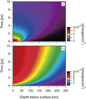
Fig. 2. Differential density distributions between the photogenerated electrons and holes estimated from numerical simulations according to a 1D DDE model. Here, we defined that the laser pulse peak reached the sample surface at t = 0.3 ps. The positive charge density in this figure represents that the hole density is higher than the electron density. We compared the differential density distributions calculated with the diffusion coefficients of De = 600 and Dh = 10 cm2/s, including the carrier drift motion induced by the resultant Dember field (a), to that calculated without the carrier drift motion but with the same diffusion condition (b). The laser irradiation conditions of 100 fs and 1 × 10⁹ W/cm2 are the same as those in the experiment.
Download figure:
Standard image High-resolution imageUsing the simulation of the differential carrier density, we calculated the temporal evolution of the surface potential  for comparison with the transient Ga-3d peak shift observed in our measurement (Fig. 3). As clearly shown in Fig. 3(b), the calculated surface potential change under a moderate temperature (Te = 950 K and Th = 300 K) probably reproduced the experimental results. For comparison, we also plotted the simulation results at the electron temperatures of Te = 1100 K and Th = 800 K, as shown in Fig. 3(b). These results roughly explain the experimental results within the error. Here, we assumed the hole temperature to be room temperature because it should be well below the electron temperature, as discussed above. Because the electron diffusion coefficient mainly depends on the electron mobility μe, which is far higher than the hole mobility μh, the hole temperature has a minor effect on the simulation results. In Fig. 3(a), at a high temperature (Te = Th = 1900 K), the surface potential significantly exceeds the experimental value, although the rising time is similar to that in the experimental results. As indicated by Fig. 2(b), when we disregarded the drift motion, the surface potential increased monotonically and exceeded 5 eV. This does not wholly agree with the experimental results, thus suggesting that the induced Dember field, whose direction is opposite to the diffusion direction, plays an important role in suppressing the carrier transport with diffusion. Therefore, the initial rapid increase in the surface-potential change observed in our experiment is most likely to correspond to the time at which the diffusion currents and drift currents induced by the Dember field reach an equilibrium state. In addition, it should be noted that the calculated result at room temperature is similar to the experimental result, although the equilibrium surface potential is clearly lower than the experimental value. This is probably because the carriers were moderately thermalized by the excess energy of the photogenerated carriers arising from the fact that the photon energy of the pump laser (1.57 eV) is slightly higher than the band-gap energy of GaAs (1.43 eV). In fact, the electron temperature is roughly estimated to be 1060 K, when approximated from the excess energy 3/2kBTe ∼ (hν − Eg). This simple estimation agrees with the electron temperature obtained from the comparison between the experimental and simulation results. Thus, the above consideration well supports the validity of the scenario wherein the transient Ga-3d peak shift observed in the experiment results from the photo-Dember effect at a moderate electron temperature of roughly 800 to 1100 K.

Download figure:
Standard image High-resolution image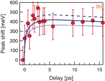
Fig. 3. The surface potential was calculated at various carrier temperatures (a): room temperature, Te = Th = 300 K (green), a moderate temperature, Te = 950 K and Th = 300 K (red), a high temperature, Te = Th = 1900 K (blue), and a moderate temperature (Te = 950 K and Th = 300 K) without the drift motion, i.e., ve = vh = 0 (gray). The experimental results were obtained with a Ga-3d peak shift as a function of the time delay (b). Three numerical simulations with moderate temperatures of Te = 800 K and Th = 300 K (blue dotted line), Te = 950 K and Th = 300 K (blue solid line), and Te = 1100 K and Th = 300 K (blue dashed line), are also plotted for comparison with the experimental results in (b).
Download figure:
Standard image High-resolution image
Finally, we briefly discuss the relaxation of the photogenerated carriers. In our experiment, no clear relaxation of the Ga-3d peak shift was observed within a time delay of 15 ps [Fig. 3(b)]. This long relaxation time contrasts the 7 ps relaxation time for n-type GaAs and 15 ps relaxation time for p-type GaAs from previous reports.18,23) Although the cause of this discrepancy is presently unclear, one possible reason is that the carrier scattering in doped semiconductors is likely to be far stronger than that in semi-insulating semiconductors, thus resulting the long relaxation time observed in our measurement. A further systematic investigation is needed for a comprehensive understanding of the surface-potential dynamics.
In summary, we investigated the initial time evolution of the surface potential on semi-insulating GaAs(001) by combining the time-resolved core-level PES experiment and numerical simulations using a standard DDE model for the transport dynamics of the photogenerated carriers. The time-resolved core-level PES enabled us to directly measure the transient modification of the surface potential using the core-level photoelectron peak shift with a femtosecond resolution. We clarified that the temporal shift of the Ga-3d-core level photoelectron peak by ∼350 meV toward a higher binding energy can be attributed to the transient surface potential induced by the Dember effect. The core-level surface PES technique with femtosecond resolution will be a promising tool for investigating ultrafast dynamics on not only semiconductor surfaces corresponding to a few atomic layers but also a wide variety of single-layer materials, such as graphene and its related materials, as well as transition metal dichalcogenides.
Acknowledgments
We thank Professor Takeda, Professor Katayama (Yokohama National University), and Dr. H. Yamamoto (NTT BRL) for helpful discussions regarding surface PES, as well as Dr. Y. Furukawa (RIKEN) for providing photoelectron detection processing software. This work was partly financed by the Ministry of Education, Culture, Sports, Science and Technology of Japan under Grant-in-Aid for Scientific Research No. 23310086.