

Summary
A protocol for graphene-assisted growth of high-quality AlN films on nano-patterned sapphire substrate is presented.
Abstract
This protocol demonstrates a method for graphene-assisted quick growth and coalescence of AlN on nano-pattened sapphire substrate (NPSS). Graphene layers are directly grown on NPSS using catalyst-free atmospheric-pressure chemical vapor deposition (APCVD). By applying nitrogen reactive ion etching (RIE) plasma treatment, defects are introduced into the graphene film to enhance chemical reactivity. During metal-organic chemical vapor deposition (MOCVD) growth of AlN, this N-plasma treated graphene buffer enables AlN quick growth, and coalescence on NPSS is confirmed by cross-sectional scanning electron microscopy (SEM). The high quality of AlN on graphene-NPSS is then evaluated by X-ray rocking curves (XRCs) with narrow (0002) and (10-12) full width at half-maximum (FWHM) as 267.2 arcsec and 503.4 arcsec, respectively. Compared to bare NPSS, AlN growth on graphene-NPSS shows significant reduction of residual stress from 0.87 GPa to 0.25 Gpa, based on Raman measurements. Followed by AlGaN multiple quantum wells (MQWS) growth on graphene-NPSS, AlGaN-based deep ultraviolet light-emitting-diodes (DUV LEDs) are fabricated. The fabricated DUV-LEDs also demonstrate obvious, enhanced luminescence performance. This work provides a new solution for the growth of high quality AlN and fabrication of high performance DUV-LEDs using a shorter process and less costs.
Introduction
AlN and AlGaN are the most essential materials in DUV-LEDs1,2, which have been widely used in various fields such as sterilization, polymer curing, biochemical detection, non-line-of-sight communication, and special lighting3. Due to the lack of intrinsic substrates, AlN heteroepitaxy on sapphire substrates by MOCVD has become the most common technical route4. However, the large lattice mismatch between AlN and sapphire substrate leads to stress accumulation5,6, high density dislocations, and stacking faults7. Thus, the internal quantum efficiency of LEDs are reduced8. In recent decades, using patterned sapphire as substrates (PSS) to induce AlN epitaxial lateral overgrowth (ELO) has been proposed to solve this problem. In addition, great progress has been made in the growth of AlN templates9,10,11. However, with a high surface adhesion coefficient and bonding energy (2.88 eV for AlN), Al atoms have low atomic surface mobility, and the growth of AlN tends to have a three-dimensional island growth mode12. Thus, the epitaxial growth of AlN films on NPSS is difficult and requires higher coalescence thickness (over 3 μm) than that on flat sapphire substrates, which causes longer growth time and requires high costs9.
Recently, graphene shows great potential for use as a buffer layer for AlN growth due to its hexagonal arrangement of sp2 hybridized carbon atoms13. In addition, the quasi-van der Waals epitaxy (QvdWE) of AlN on graphene may reduce the mismatch effect and has paved a new way for AlN growth14,15. To increase the chemical reactivity of graphene, Chen et al. used N2-plasma treated graphene as a buffer layer and determined the QvdWE of high quality AlN and GaN films8, which demonstrates the utilization of graphene as a buffer layer.
Combining the N2-plasma treated graphene technic with commercial NPSS substrates, this protocol presents a new method for quick growth and coalescence of AlN on a graphene-NPSS substrate. The completely coalesce thickness of AlN on graphene-NPSS is confirmed to be less than 1 µm, and the epitaxial AlN layers are of high quality and stress-released. This method paves a new way for AlN template mass production and shows great potential in the application of AlGaN-based DUV-LEDs.
Subscription Required. Please recommend JoVE to your librarian.
Protocol
CAUTION: Several of the chemicals used in these methods are acutely toxic and carcinogenic. Please consult all relevant material safety data sheets (MSDS) before use.
1. Preparation of NPSS by nanoimprint lithography (NIL)
- Deposition of SiO2 film
- Wash the 2" c-plane flat sapphire substrate with ethanol followed by deionized water three times.
- Dry the substrate with a nitrogen gun.
- Deposit 200 nm SiO2 film on the flat sapphire substrate by plasma-enhanced chemical vapor deposition (PECVD) under 300 °C. The deposition rate is 100 nm/min.
- Spinning nanoimprint resist
- Wash the sapphire substrate with ethanol followed by deionized water 3x.
- Dry the substrate with a nitrogen gun.
- Spin a 200 nm nanoimprint resist (NIR) TU-2 on the flat sapphire substrate at 3000 r/min for 60 s.
- Thermoplastic imprinting
- Place a patterned mold onto the nanoimprint resist polymer film.
- Apply high pressure as 30 bar at 60 °C to heat the sapphire substrate to above the glass transition temperature of the polymer.
- Expose to ultraviolet irradiation for 60 s and maintain for 120 s after turning off the UV source to solidify the NPR TU-2.
- Cool down the sapphire substrate and mold to room temperature (RT).
- Release the mold.
- Pattern transfer
- Etch the sapphire substrate exposed from the nano-holes on the NIR by inductive coupled plasma reactive ion etching (ICP-RIE) with BCl3 to transfer the pattern onto the sapphire substrate. The etching power is 700 W and etching time is 3 min.
- Remove the residual NPR TU-2 by O2 plasma etching in a RIE system for 20 s. The etching pressure is 5 mTorr and etching power is 100 W. Finally, the width of the unetched regions is 300 nm and the depth is 400 nm. The period of pattern is 1 μm.
NOTE: NIL is not the only way to get NPSS. The NPSS are commercialized and could be bought elsewhere.
2. APCVD growth of graphene on NPSS
- Rinse the NPSS with acetone, ethanol, and deionized water 3x.
- Dry the NPSS with a nitrogen gun.
- Load the NPSS into a three-zone high temperature furnace for long, flat temperature zone. Heat the furnace to 1050 °C and stabilize for 10 min under 500 sccm Ar and 300 sccm H2
- Introduce 30 sccm CH4 into the reaction chamber for the growth of graphene on NPSS for 3 h. After the growth of graphene, switch off the CH4 and naturally cool.
3. N2-plasma treatment
- Rinse the graphene-NPSS with deionized water.
- Dry the NPSS with a nitrogen gun.
- Etch the graphene-NPSS by N2-plasma with a N2 flow rate of 300 sccm for 30 s and power of 50 W in a reactive ion etching (RIE) chamber.
4. MOCVD growth of AlN on graphene-NPSS
- Edit the MOCVD recipe for AlN growth and load the graphene-NPSS and its NPSS counterpart into the homemade MOCVD chamber.
- After heating for 12 min, the temperature is stabilized at 1200 °C. Introduce 7000 sccm H2 as ambient, 70 sccm trimethylaluminum (TMAl), and 500 sccm NH3 for the growth of AlN for 2 h.
5. MOCVD growth of AlGaN MQWs
- Lower the temperature of MOCVD chamber to 1130 °C to grow 20-period AlN (2 nm)/Al0.6Ga0.4N (2 nm) layer superlattice (SL) with periodic changes in TMAl flow to adjust the deposition component. The ambient gas is H2. The mole flow rates of TMAl, TMGa, and NH3 for AlN are 50 sccm, 0 sccm, and 1000 sccm; and for AlGaN are 32 sccm, 7 sccm, and 2,500 sccm, respectively.
- Lower the temperature of MOCVD chamber to 1002 °C and introduce a silicane flow for the growth of a 1.8 µm n-Al0.55Ga0.45N layer. The ambient gas is H2 and concentration of n-type AlGaN is 5 x 1018 cm-3.
- Grow 5-period Al0.6Ga0.4N (3 nm)/Al0.5Ga0.5N (12 nm) MQWs by switching the TMAl from 24 sccm to 14 sccm, and TMGa from 7 sccm to 8 sccm, for each period at 1002 °C. The ambient gas is H2.
- Deposit 50 nm Mg-doped p- Al0.65Ga0.35N electron blocking layer (EBL) at 1002 °C. The mole flow rates of TMAl, TMGa, and NH3 are 40 sccm, 6 sccm, and 2500 sccm. The ambient gas is H2.
- Deposit 30 nm p-Al0.5Ga0.5N cladding layer with NH3 flow of 2500 sccm. The ambient gas is H2.
- Deposit 150 nm p-GaN contact layer with an NH3 flow of 2500 sccm. The ambient gas is H2. The mole flow rates of TMGa and NH3 are 8 sccm and 2500 sccm. The hole concentration of p-AlGaN is 5.4 x 1017 cm-3.
- Lower the temperature of MOCVD chamber to 800 °C and anneal the p-type layers with N2 for 20 min. The ambient gas is N2.
6. Fabrication of AlGaN-based DUV-LEDs
- Spinning photoresist 4620 on the wafers and lithography. The UV exposure time, developing time, and rinsing time are 8 s, 30 s, and 2 min, respectively.
- ICP etching of p-GaN. The etching power, etching pressure, and etching rate of GaN are 450 W, 4 m Torr, and 5.6 nm/s, respectively.
- Put the sample into acetone at 80 °C for 15 min followed by washing the sample with ethanol and deionized water 3x.
- Spinning negative photoresist NR9 and lithography. The UV exposure time, developing time, and rinsing time are 12 s, 20 s, and 2 min, respectively.
- Wash the sample with acetone, ethanol, and deionized water 3x.
- Deposit Ti/Al/Ti/Au by electron beam (EB) evaporation.
- Spin negative photoresist NR9 and lithography. The UV exposure time, developing time, and rinsing time are 12 s, 20 s, and 2 min, respectively.
- Wash the sample with acetone, ethanol, and deionized water 3x without ultrasonication.
- Deposit Ni/Au by EB evaporation.
- Wash the sample with ethanol and deionized water 3x to clean the sample.
- Deposit 300 nm SiO2 by plasma enhanced chemical vapor deposition (PECVD). The deposition temperature is 300 °C and deposition rate is 100 nm/min.
- Spin photoresist 304 and lithography. The UV exposure time, developing time, and rinsing time are 8 s, 1 min, and 2 min, respectively.
- Immerse the wafers into 23% HF solution for 15 s.
- Wash the sample with ethanol and deionized water 3x and dry with a nitrogen gun.
- Deposit Al/Ti/Au by EB evaporation after photolithography. The photolithography process is the same as that performed in steps 6.4-6.7.
- Wash the sample with ethanol and deionized water 3x.
- Grind and polish the sapphire to 130 µm by mechanical polishing.
- Wash the sample with dewaxing solution and deionized water.
- Cut the whole wafer into pieces of 0.5 mm x 0.5 mm devices with a laser and cut it into chips using a mechanical dicer.
Subscription Required. Please recommend JoVE to your librarian.
Representative Results
Scanning electron microscopy (SEM) images, X-ray diffraction rocking curves (XRC), Raman spectra, transmission electron microscopy (TEM) images, and electroluminescence (EL) spectrum were collected for the epitaxial AlN film (Figure 1, Figure 2) and AlGaN-based DUV-LEDs (Figure 3). The SEM and TEM are used to determine the morphology of the AlN on graphene-NPSS. XRD and Raman are used to calculate the dislocation densities and the residual stress. EL is used to illustrate the illumination of the fabricated DUV-LEDs.

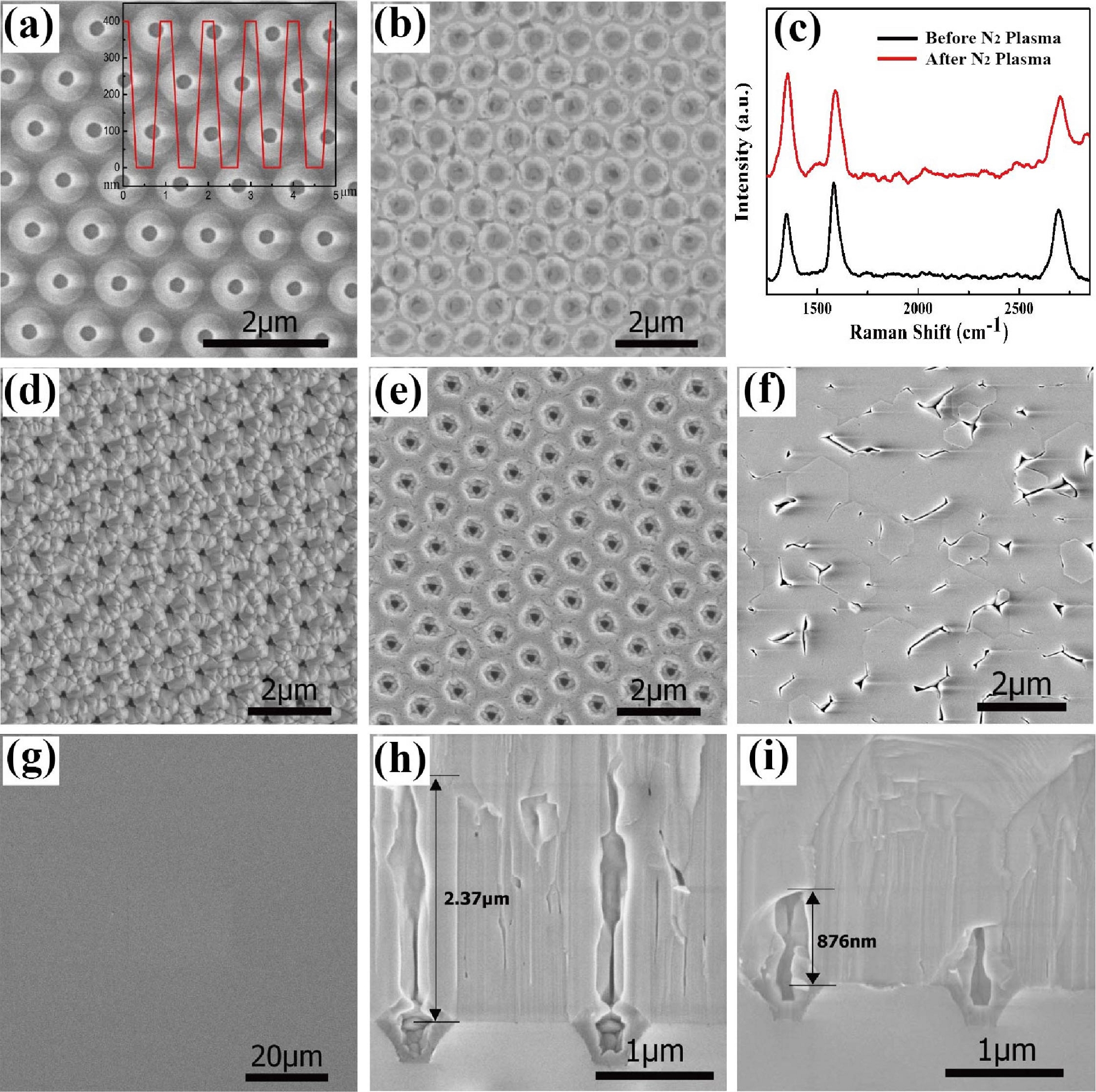
Figure 1: Growth of AlN film on N2 plasma-treated graphene-NPSS substrate.
(A) SEM image of the bare NPSS. The inset shows the line profile of the patterns of NPSS by AFM. (B) SEM image of the as-grown graphene films on NPSS. (C) Raman spectra of graphene film before N2 plasma treatment (black) and after N2 plasma treatment (red). (D, F) are the SEM images of the initial 10 min and 2 h growth of AlN films on NPSS without graphene interlayer. (E and G) are the SEM images of the initial 10 min and 2 h growth AlN films on NPSS with graphene interlayer. (H, I) are the cross-sectional SEM images of AlN films on NPSS without and with graphene interlayer. This figure has been modified from Chang et al.20. Please click here to view a larger version of this figure.

Figure 2: The characterization of AlN grown on N2 plasma-treated graphene-NPSS substrate.
XRC of (A) (0002) and (B) (102) for AlN films grown on NPSS with and without graphene interlayer. (C) Raman spectra of AlN layers grown on NPSS with and without graphene interlayer. (D) HRTEM image of the AlN/ graphene/NPSS interface. (E, F) are the SAED patterns taken from the AlN layer and interface between AlN and graphene/NPSS. (G) Bright-field cross-sectional TEM images of AlN grown on graphene/NPSS with g = [0 10]. This figure has been modified from Chang et al.20. Please click here to view a larger version of this figure.

Figure 3: The performance of as-fabricated DUV-LED.
(A) Schematic diagram of the AlGaN-based DUV-LED structure. (B) EL spectra of the DUV-LEDs with and without graphene interlayer. This figure has been modified from Chang et al.20 Please click here to view a larger version of this figure.
Subscription Required. Please recommend JoVE to your librarian.
Discussion
As shown in Figure 1A, the NPSS prepared by the NIL technique illustrates the nano-concave cone patterns with 400 nm depth, 1 μm period of pattern, and 300 nm width of the unetched regions. After the APCVD growth of graphene layer, the graphene-NPSS is shown in Figure 1B. The significant increased D peak of N-plasma treated graphene in Raman spectra Figure 1C demonstrates the increase of dangling bonds generated during the RIE process16. After directly MOCVD growth of AlN for 10 min, Figure 1D shows 3D growth of irregular AlN islands on bare NPSS while Figure 1E shows a lateral 2D manner and rapid coalescence of AlN on graphene-NPSS. After 2 h of growth, the surface of AlN film on graphene-NPSS becomes continuous and flat (Figure 1G) due to the quick lateral growth and rapid coalescesence of AlN on graphene. On the contrary, Figure 1F shows the rough surface of AlN directly grown on bare NPSS. Also, from the cross-sectional SEM images of the as-grown AlN on NPSS and graphene-NPSS shown in Figure 1H,I, it is clear that with the assist of the graphene interlayer, AlN displays quick coalescence on graphene-NPSS.
The (0002) and (102) XRC of AlN films shown in Figure 2A,B confirms the high quality of the AlN grown on graphene-NPSS, with significantly reductions in FWHM XRC from 455.4 arcsec to 267.2 arcsec and 689.2 arcsec to 503.4 arcsec, respectively, compared to AlN grown on bare NPSS. Thus, the estimated densities of screw dislocations of AlN on bare NPSS is 4.51 x 108 cm-2, which is reduced to 1.55 x 108 cm-2 with the assistance of graphene. These results show improvement quality of AlN on NPSS with a graphene buffer, which is more suitable for DUV-LEDs17.
The Raman spectrum of E2 phonon mode of AlN (Figure 2C), which is sensitive to the biaxial stress18, demonstrates stress-released AlN on graphene-NPSS with the E2 peak located at 658.3 cm-1, closer to the stress-free AlN (657.4 cm-1), compared to AlN on the bare NPSS (660.6 cm-1). The residual stress estimated based on Raman spectra shows significantly reduced from 0.87 GPa to 0.25 GPa with the assistance of graphene.19
Figure 2D shows an HRTEM image of the AlN/graphene/NPSS interface with smooth epitaxy of AlN on NPSS with the assistance of graphene, indicating quasi-van der Waals epitaxy of AlN. Figure 2E shows the selected area electron diffraction (SAED) pattern of the AlN, demonstrating that the as-grown AlN on graphene-NPSS is wurtzite structure. The crystal orientation is along the c-axis. As shown in Figure 2F, the orientation relationship of AlN and Al2O3 is as follows: (0002) AlN/(0006) Al2O3 and (010) AlN/( 20) Al2O3. Figure 2G shows the forming of air void over the cones during the lateral growth of AlN. Some dislocations near the void bend and annihilate at the climax of void; thus, the threading dislocation density of AlN is reduced. The TEM measurements explain the released stress and reduced dislocation density of AlN on graphene due to QvdWE growth.
EL spectrum (Figure 3B) of AlGaN-based DUV-LEDS on graphene-NPSS shows 2.6x stronger luminescence at a peak wavelength of 280 nm and current of 40 mA, compared to that of bare NPSS. The protocol demonstrates a method for the growth of high quality stress-released AlN films on NPSS with the assistance of CVD-growth graphene interlayer by MOCVD. N2 plasma treatment enhances the chemical reactivity of graphene and realizes QvdWE growth of AlN. However, the selective growth of graphene on NPSS still warrants in-depth studies. Using this method, the growth and coalescence rates of AlN on NPSS are also increased, which is essential for mass production with lower cost and shortened time requirements. The AlN template grown on graphene-NPSS shows great potential in the application of AlGaN-based DUV-LEDs.
Subscription Required. Please recommend JoVE to your librarian.
Disclosures
The authors have nothing to disclose.
Acknowledgments
This work was financially supported by the National Key R&D Program of China (No. 2018YFB0406703), the National Natural Science Foundation of China (Nos. 61474109, 61527814, 11474274, 61427901), and the Beijing Natural Science Foundation (No. 4182063)
Materials
| Name | Company | Catalog Number | Comments |
| Acetone,99.5% | Bei Jing Tong Guang Fine Chemicals company | 1090 | |
| APCVD | Linderberg | Blue M | |
| EB | AST | Peva-600E | |
| Ethonal,99.7% | Bei Jing Tong Guang Fine Chemicals company | 1170 | |
| HF,40% | Beijing Chemical Works | 1789 | |
| ICP-RIE | AST | Cirie-200 | |
| MOCVD | VEECO | P125 | |
| PECVD | Oerlikon | 790+ | |
| Phosphate,85% | Beijing Chemical Works | 1805 | |
| Sulfuric acid,98% | Beijing Chemical Works | 10343 |
References
- Sakai, Y., et al. Demonstration of AlGaN-Based Deep-Ultraviolet Light-Emitting Diodes on High-Quality AlN Templates. Jappanese Journal of Applied Physics. 49, 022102 (2010).
- Yun, J., Hirayama, H. Investigation of the light-extraction efficiency in 280 nm AlGaN-based light-emitting diodes having a highly transparent p-AlGaN layer. Journal of Applied Physics. 121, 013105 (2017).
- Khan, A., Balakrishnan, K., Katona, T. Ultraviolet light-emitting diodes based on group three nitrides. Nature Photonics. 2, 77-84 (2008).
- Balushi, Z. Y. A., et al. The impact of graphene properties on GaN and AlN nucleation. Surface Science. 634, 81-88 (2015).
- Motoki, K., et al. Growth and characterization of freestanding GaN substrates. Journal of Crystal Growth. 237, 912-921 (2002).
- Kim, Y., et al. Remote epitaxy through graphene enables two-dimensional material-based layer transfer. Nature. 544, 340-343 (2017).
- Hemmingsson, C., Pozina, G. Optimization of low temperature GaN buffer layers for halide vapor phase epitaxy growth of bulk GaN. Journal of Crystal Growth. 366, 61-66 (2013).
- Chen, Z., et al. High-Brightness Blue Light-Emitting Diodes Enabled by a Directly Grown Graphene Buffer Layer. Advanced Materials. 30, 1801608 (2018).
- Dong, P., et al. 282-nm AlGaN-based deep ultraviolet light-emitting diodes with improved performance on nano-patterned sapphire substrates. Applied Physics Letters. 102, 241113 (2013).
- Imura, M., et al. Epitaxial lateral overgrowth of AlN on trench-patterned AlN layers. Journal of Crystal Growth. 298, 257-260 (2007).
- Kueller, V., et al. Growth of AlGaN and AlN on patterned AlN/sapphire templates. Journal of Crystal Growth. 315, 200-203 (2011).
- Kneissl, M., et al. Advances in group III-nitride-based deep UV light-emitting diode technology. Semiconductor Science & Technology. 26, 014036 (2010).
- Kunook, C., Chul-Ho, L., Gyu-Chul, Y. Transferable GaN layers grown on ZnO-coated graphene layers for optoelectronic devices. Science. 330, 655-657 (2010).
- Kim, J., et al. Principle of direct van der Waals epitaxy of single-crystalline films on epitaxial graphene. Nature Communications. 5, 4836 (2014).
- Han, N., et al. Improved heat dissipation in gallium nitride light-emitting diodes with embedded graphene oxide pattern. Nature Communications. 4, 1452 (2013).
- Gupta, P., et al. MOVPE growth of semipolar III-nitride semiconductors on CVD graphene. Journal of Crystal Growth. 372, 105-108 (2013).
- Heinke, H., Kirchner, V., Einfeldt, S., Hommel, D. X-ray diffraction analysis of the defect structure in epitaxial GaN. Appllied Physics Letters. 77, 2145-2147 (2000).
- Lughi, V., Clarke, D. R. Defect and Stress Characterization of AlN Films by Raman Spectroscopy. Appllied Physics Letters. 89, 2653 (2006).
- Li, Y., et al. Van der Waals epitaxy of GaN-based light-emitting diodes on wet-transferred multilayer graphene film. Jappanese Journal of Applied Physics. 56, 085506 (2017).
- Chang, H., et al. Graphene-assisted quasi-van der Waals epitaxy of AlN film for ultraviolet light emitting diodes on nano-patterned sapphire substrate. Applled Physics Letters. 114, 091107 (2019).
