
Abstract
Far-UV light sources have attracted much attention for human-safe viral inactivation and bacterial disinfection. Due to large optical nonlinearity and transparency to this wavelength region, AlN is a promising material for compact and low-cost far-UV second harmonic generation (SHG) devices. In this study, a transverse quasi-phase-matched AlN channel waveguide with vertical polarity inversion was designed and fabricated. From wavelength spectra and a pump power dependence of an SH intensity, far-UV SHG via the largest nonlinear optical tensor component d33 was successfully confirmed under ultrashort pulse laser excitation.
Export citation and abstract BibTeX RIS

Content from this work may be used under the terms of the Creative Commons Attribution 4.0 license. Any further distribution of this work must maintain attribution to the author(s) and the title of the work, journal citation and DOI.
UV light sources are used in various fields, such as inactivation and disinfection, sensing, and material processing. In recent years, far-UV light in a wavelength range of 210–230 nm has attracted considerable attention for viral inactivation and bacterial disinfection without harm to exposed human skin and eyes owing to strong absorption on non-living surface tissues. 1–3) Excimer lamps at a wavelength of 222 nm are commercially available, however, they have disadvantages, such as the use of expensive gases, low efficiency, and short lifetime. The efficiency of LEDs drops sharply at a wavelength shorter than 250 nm. 4) However, an LED with the shortest emission wavelength at 210 nm 5) has been achieved using AlN 5) with a wide bandgap of ≈6.0 eV. 6,7) To date, the shortest lasing wavelength for AlGaN laser diodes (LDs) is 271.8 nm. 8) The difficulty in far-UV LEDs and LDs is due to the insulating nature of AlGaN. Therefore, the development of novel far-UV light sources is crucial.
Wavelength conversion is another technology to realize far-UV light sources. Far-UV wavelength conversion systems using bulk crystals, such as β-BaB2O4 (BBO) and CsLiB6O10 (CLBO), 9,10) are widely used for industrial applications. Although the nonlinear optical constants of these crystals are small, high conversion efficiency is realized under high-power excitation. In waveguide devices with quasi-phase-matched (QPM) structures which has periodic polarity inversion in the longitudinal direction, the high normalized conversion efficiency can be obtained due to long interaction lengths while maintaining high-power density even under low power excitation. These devices for a wavelength longer than 300 nm were usually made of ferroelectric crystals, such as LiNbO3 and LiTaO3, because of their large optical nonlinearity. 11–13) Although LaBGeO5 is transparent down to a wavelength of 190 nm, high-efficiency wavelength conversion cannot be realized due to small optical nonlinearity. 14)
AlN is an attractive material owing to its large optical nonlinearity 15) and transparency to far-UV light. UV second harmonic generation (SHG) at 306 nm in an AlN waveguide with a thickness satisfying a modal dispersion phase matching (MDPM) condition has been demonstrated without the QPM structure. 16) In order to increase the conversion efficiency, a third-order QPM structure was fabricated in the AlN channel waveguide and UV SHG at 344 nm was demonstrated. 17) While AlN waveguides with first-order QPM structures for 250–275 nm UV light were fabricated, 18,19) SHG has not been reported so far. The wavelength conversion efficiency can be enhanced by employing a vertically polarity-inverted multilayer structure satisfying the MDPM condition, 20,21) which is called a transverse QPM structure. In our previous work, blue SHG at 438 nm was demonstrated from the transverse QPM GaN channel waveguide. 22) Vertical polarity inversion of AlN layers by epitaxial growth has been reported. 23–25) In this study, a transverse QPM SHG channel waveguide with a vertically polarity inverted AlN bilayer was designed. From the channel waveguide consisting of a −c/+c-AlN bilayer fabricated by sputtering and post-deposition face-to-face annealing (FFA), 24) 229 nm far-UV SHG was successfully demonstrated.
A schematic of the transverse QPM SHG device with a vertically polarity inverted AlN bilayer is shown in Fig. 1. A channel waveguide consists of upper −c-AlN and lower +c-AlN layers on a c-plane sapphire substrate. Even though a slight reduction of optical confinement occurs, a SiO2 cladding layer is necessary to protect the channel waveguide during the formation of the end faces. The cross-sectional dimension of the channel waveguide was designed to satisfy the MDPM condition between a fundamental wave of a first-order TM00-guided mode and an SH wave of a high-order TM0q
mode. The TM-polarized fundamental wave was chosen for utilizing the largest nonlinear optical tensor component d33 of AlN, and the TM-polarized SH wave was generated. The electric field distributions in the y-axis direction for the fundamental wave Eω
(x, y) and SH wave E2ω
(x, y) are shown in Fig. 1. When the MDPM condition is satisfied, the wavelength conversion efficiency η can be calculated as  where κ is the nonlinear coupling coefficient, L is the waveguide length, and P0 is the fundamental wave power in the waveguide.
26)
κ is calculated by
where κ is the nonlinear coupling coefficient, L is the waveguide length, and P0 is the fundamental wave power in the waveguide.
26)
κ is calculated by

where ω is the angular frequency of the fundamental wave; ε0 is the dielectric constant in vacuum and d33(x, y) is the distribution of the nonlinear optical constant. The coordinates are shown in Fig. 1. The overlap integral in Eq. (1) represents how strongly Eω and E2ω are coupled via d33. Because the positive and negative antinodes of E2ω cancel the integral in Eq. (1), κ is small for a single AlN layer with constant d33. By polarity inversion of the AlN layer at an appropriate position to modify the sign of d33, κ can be significantly increased. According to Eq. (1), κ is maximized when the polarity is inverted at all node positions of E2ω . Due to the difficulty in the fabrication of multiple-polarity inverted structures, this study discusses κ for the polarity inverted AlN bilayer channel waveguide. Polarity inversion at a node close to the peak of Eω (around the center of the channel waveguide in the y-direction) enhances κ efficiently.

Fig. 1. Schematic of transverse QPM SHG device with vertical polarity inverted AlN bilayer.
Download figure:
Standard image High-resolution imageThe effective refractive indices and electric field distributions of the fundamental and SH-guided modes were calculated by the finite difference method. 27) The wavelength dispersions of the refractive indices for the −c/+c-AlN bilayer and a SiO2 layer deposited by plasma-enhanced chemical vapor deposition (PECVD) were measured by a spectroscopic ellipsometer, assuming that the refractive index of the AlN layer was independent of the polarity. As the measurement range of the spectroscopic ellipsometer was from 245 nm to 1000 nm, the refractive indices were extrapolated to 230 nm based on the Cauchy model. The refractive index of the sapphire substrate was based on the literature values. 28) The dependences of the effective refractive indices of the first-order fundamental and high-order SH modes on the waveguide thickness for a channel waveguide width of 0.6 μm are shown in Fig. 2(a). The waveguide thicknesses satisfying the MDPM conditions between the fundamental TM00 mode and the SH TM02, TM03, and TM04 modes were estimated to be 176, 269, and 358 nm, respectively. The largest κ values for the TM02, TM03, and TM04 mode SH waves were calculated as 5.9, 6.2, and 4.2 W−1/2 cm−1 when the polarity inversion positions from the AlN/sapphire interface were 47, 129, and 135 nm, respectively. κ for these SH waves in the AlN single-layer channel waveguide were 0.9, 0.1, and 0.3 W−1/2 cm−1. Macroscopic defects tend to emerge on the surface of a thin AlN layer grown by sputtering and post-deposition FFA. 24,29) Therefore, the SH TM04 mode was employed to prevent macroscopic defects. As shown in the inset of Fig. 2(b), E2ω for the SH TM04 mode has two nodes close to the center of the channel waveguide. To investigate the second largest κ and a position error tolerance, the dependence of κ on the polarity inversion position between the fundamental TM00 and SH TM04 modes was calculated as shown in Fig. 2(b). It shows that κ is obtained as large as 4.0 W−1/2 cm−1 for the polarity inversion position of 213 nm and a 10 nm position error gives an 8% reduction of κ.
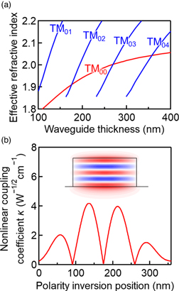
Fig. 2. (a) Dependences of effective refractive indices of fundamental (red line) and SH (blue lines) modes on waveguide thickness for waveguide width of 0.6 μm. (b) Dependence of nonlinear coupling coefficient κ between fundamental TM00 and SH TM04 modes on polarity inversion position. Inset shows the electric field distribution of SH TM04 mode.
Download figure:
Standard image High-resolution imageThe fabrication process is illustrated in Fig. 3. As reported in Ref. 24 the polarity of the FFA sputtered AlN layer can be controlled by changing sputtering targets, and an abrupt polarity inversion domain boundary (IDB) of a fabricated −c/+c-AlN bilayer was observed using scanning transmission electron microscopy. (a) A 210 nm-thick +c-AlN layer was deposited on a c-plane sapphire substrate by radio frequency (RF) sputtering with a sintered AlN target. 29) An FFA of the sample was performed at 1700°C in a nitrogen atmosphere to improve its crystallinity. 30) Then, a 280 nm-thick −c-AlN layer was deposited by RF sputtering with a metallic Al target on the +c-AlN layer, followed by a second post-deposition FFA. 24) (b) The AlN bilayer was thinned by inductively coupled plasma-reactive ion etching (ICP-RIE) using Cl2 and BCl3 gases. BCl3 gas was used to remove unintentionally formed oxides at the surface. 31,32) The antenna and bias powers were set at 250 and 10 W, respectively, which are lower than those used in the channel formation process to reduce the etching rate for accurate thickness control. The thickness was carefully adjusted by alternating between ICP-RIE etching and thickness measurements using the spectroscopic ellipsometer. A polarity-inverted −c-AlN/+c-AlN layer with a thickness of 352 nm was obtained. Another chip from the same wafer was used for surface roughness measurement. After ICP-RIE under the same condition, a root mean square surface roughness measured by an atomic force microscope for a 5 × 5 μm2 area was slightly increased from 0.3 nm to 2.4 nm. It would not cause a large waveguide loss. (c) A 200 nm-thick SiO2 layer was deposited by PECVD. A negative EB resist was used to form the channel patterns by EB lithography. The SiO2 masks were formed by capacitively coupled plasma RIE (CCP-RIE) using CF4/H2 gas. (d) The channel waveguides were formed by ICP-RIE at antenna and bias powers of 400 and 50 W, respectively. Relatively smooth sidewalls were obtained. Since lateral optical confinement of the TM mode is strong in the channel waveguide, the influence of the sidewall roughness on the waveguide loss is considered to be small. The waveguide loss needs to be evaluated in the future. (e) A 1 μm thick SiO2 cladding layer was deposited by PECVD and the end faces of the channel waveguides were formed by dicing and polishing with diamond slurry. The length of the fabricated waveguide was approximately 2 mm. From the cross-sectional SEM image shown in Fig. 3(f), the top edge of the waveguide was slightly chipped and the sidewall angle of the AlN channel waveguide was approximately 70° due to low etching selectivity. The sidewall angle of 70° gives little influence on the phase matching wavelength and κ.
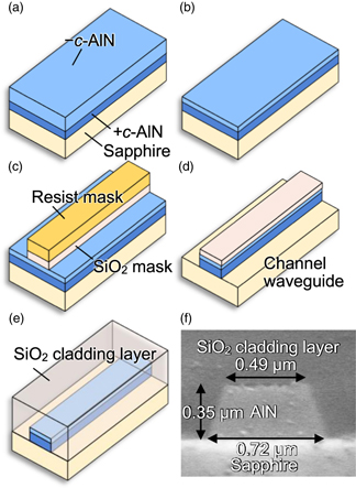
Fig. 3. Fabrication process of a transverse QPM SHG device with a vertical polarity inverted AlN bilayer. (a) Sputtering and post-deposition FFA of polarity-inverted AlN bilayer. (b) Adjustment of AlN layer thickness. (c) Formation of SiO2 mask. (d) Formation of the channel waveguide. (e) Deposition of SiO2 cladding layer, dicing, and end face polishing. (f) Cross-sectional SEM image of the fabricated channel waveguide.
Download figure:
Standard image High-resolution imageOptical experiments were performed using a tunable frequency-doubled femtosecond Ti:sapphire laser with a BBO crystal as a pump source. The polarization and power of the pump light were adjusted using a half-wave plate and a Glan–Thomson prism. The laser light was focused using a 100× objective lens and coupled to the channel waveguide in TM polarization. The output light from the waveguide was coupled into an optical fiber connected to a charge-coupled device spectrometer by a Cassegrain objective and an off-axis parabolic mirror. A bandpass filter with transmittances of 40% and 0.02% for wavelengths of 230 and 460 nm, respectively, was inserted between the Cassegrain objective and the off-axis parabolic mirror. The wavelength of the pump light was set to 458 nm, and the average pump power was 1.6 mW after the 100× objective lens. From the spot diameter of about 1 μm and the pulse width of 200 fs with the repetition frequency of 80 MHz, the corresponding temporal peak power density of the pump light was estimated as 13 GW cm−2. Figure 4(a) shows the measured wavelength spectra of the pump and SH lights through the waveguide (a resolution of 0.5 nm at a wavelength of 460 nm), and a far-UV light with a central wavelength of 229 nm was obtained. The full widths at half maximum of the pump and SH spectra were 2.7 nm and 1.0 nm, respectively. The wide spectral bandwidth of the SH light would be caused by group velocity walk-off between the pump and SH ultrashort pulses. 22) The peak intensity of the SH light was proportional to the square of the average pump power as shown in Fig. 4(b). Therefore, far-UV SHG in the vertical polarity inverted AlN bilayer channel waveguide was confirmed. From the wavelength spectra of the SH lights for TM- and TE-polarized pump lights as shown in Fig. 4(c), the SH intensity for the TM pump light was much stronger than that for the TE pump light. This result indicates that SHG via the nonlinear optical tensor component of d33 was achieved. The normalized wavelength conversion efficiency ηSH has not been estimated experimentally here, but is roughly estimated to be 10−4% W−1 assuming a d33 of 6.3 pm V−1 15) and no waveguide loss using the theoretical calculation reported in Ref. 22. Our quantitative efficiency determination for the case of blue SHGs from GaN transverse QPM channel waveguides with ultrashort pulse excitation indicates that ηSH should be also lower for AlN-based SHGs due to the short effective interaction length of about 20 μm, caused by the severe walk-off between the fundamental and SH wave peak positions due to group velocity dispersion. Note that with a continuous wave excitation in our ongoing experiment, significant improvement of the efficiency is expected, up to 60% W−1 for the 2 mm length device used in this study, since the effective interaction length should be extended to the entire length of the device due to perfect phase matching.

Fig. 4. (a) Wavelength spectra of the pump and SH waves. (b) Dependence of peak SH intensity on average pump power. (c) Dependence of SH wave spectra on the polarization of pump light.
Download figure:
Standard image High-resolution image
In conclusion, a transverse QPM channel waveguide was designed and fabricated using a vertical polarity inverted −c-AlN/+c-AlN bilayer, and 229 nm far-UV SHG via the largest nonlinear optical tensor component d33 was confirmed under ultrashort pulse laser pumping. The results show that the vertical polarity inverted AlN bilayer channel waveguide is a promising candidate for high-efficiency, compact, and low-cost far-UV light sources. Further optical characterization, including an SHG efficiency and a wavelength tolerance, is necessary for a detailed understanding.
Acknowledgments
This work was partly supported by JSPS KAKENHI Grant Nos. JP19H02631 and JP22H01970. We acknowledge the support of the R3 Institute for Newly-Emerging Science Design, Osaka University and the Photonics Center, Osaka University.