
Abstract
We have characterized charged states of a self-aligned Si quantum dot (QD) structure with an areal density as high as ∼1013 cm−2 by surface potential measurements by using atomic force microscopy (AFM)/Kelvin probe force microscopy (KFM). By line scanning with the electrically-biased AFM tip with respect to the substrate in a contact mode, the corresponding area was negatively charged caused by electron injection from the tip into QDs. Cross-sectional profiles of the surface potential were clearly changed, which depends on the tip bias voltages. Also, a stepwise shape in a relationship between the change of the surface potential (ΔV) and the tip bias voltages was observed, reflecting electron charging into the discrete energy levels due to the quantum confinement effect. By assuming a simple equivalent circuit model for KFM measurements of the self-aligned Si-QDs, calculated results for ΔV are in good agreement with the measured results. The agreements precisely clarified the charged states in Si-QDs.
Export citation and abstract BibTeX RIS
1. Introduction
Recently, silicon quantum dots (Si-QDs) with their unique physical properties associated with discrete charged states and/or quantum size effects at room temperature 1–6) have attracted attention since they can be applied to novel Si-based functional devices such as light-emitting diodes, 7–11) single-electron (or hole) transistors, 12–15) multi-valued metal-oxide-semiconductor memories, 16–18) electron field emission devices, 19,20) and spin-quantum bits. 21–24) So far, we have reported the self-assembling formation of Si-QDs using low-pressure chemical vapor deposition (LPCVD) with pure monosilane (SiH4) gas, 25) and demonstrated that amount of charges stored in each Si-QD can be evaluated from the surface potential changes due to electron injection to (and/or extraction from) Si-QDs using atomic force microscopy (AFM)/Kelvin probe force microscopy (KFM) techniques. 26,27) More recently, we have also succeeded in the formation of self-aligned Si-QDs for a vertical direction toward a Si(100) surface (that is to say, a dot formed on a dot) by a self-aligned process with a sequence consisting of selective Ge growth on pre-grown Si-QDs by LPCVD, in situ oxidation, thermal desorption of Ge-oxide and second Si-QDs formation. 28,29) These results indicate a possibility for flexible and controllable formation of Si-QDs even in a 3-dimensional structure. On the other hand, in the quantum devices, knowing the charged states of Si-QDs and the temporal stability of the charged states (that is to say retention time) leads to knowing the performances of the quantum devices. Therefore, investigations of the charged states and the temporal stability are quite meaningful for the improvement of the performances. Recently, we have evaluated the electrical charged states of the self-aligned Si-QDs on a ∼3.8 nm thick SiO2/Si(100) substrate after electron injection by AFM/KFM techniques and roughly quantified the number of electrons stored in the self-aligned Si-QDs by a simple equivalent circuit model in the KFM measurements. 30) In this paper, in detail, we analyzed the charged states from the surface potential of the self-aligned Si-QDs using a modified equivalent circuit model, resulting in an accuracy of the obtained results related to charging to the discrete energy levels originated from the quantum confinement effect.
2. Experimental
Chemically-cleaned n-type Si(100) with a resistivity of 8–10 Ωcm was oxidized at 1000 °C in an O2 ambient condition with a concentration of 2% to grow a ∼3.8 nm thick SiO2 film on the Si substrate surface. Here, the O2 gas was diluted with N2. After that, the substrate was slightly dipped in a diluted hydrogen fluoride solution with a concentration of 0.1% to obtain a SiO2 surface with a hydroxy (OH) group which enables us to increase nucleation sites for Si-QDs and reduce the dots size distribution. 25) Subsequently, the OH-terminated SiO2 surface was exposed to a GeH4 gas at room temperature. Here, the GeH4 gas was diluted with He, and the concentration (CG) of GeH4 was 10%. And then, domed-shaped Si-QDs with an areal dot density as high as ∼1013 cm−2 were self-assembled in the SiO2 with Si–OH bonds at 580 °C by controlling the early stages of LPCVD using 100% Si2H6 gas at a pressure of 27 Pa. 31) After that, Ge was selectively deposited on the pre-grown Si-QDs using GeH4 with CG of 5% 32) and followed by oxidation at 600 °C in a dry O2 ambient. Immediately after that, to remove surface Ge-oxide on the deposited Ge, the substrate was annealed at 1000 °C after the process chamber was evacuated down to ∼1 × 10⁻⁵ Pa. We already confirmed by high-resolution X-ray photoelectron spectroscopy 28) that the formed Si-QDs is changed to SiGe-QDs due to the high temperature. And then, to form the self-aligned Si-QDs, LPCVD was carried out again at 580 °C under a pressure of 4 Pa. Subsequently, the sample surface was oxidized at 850 °C for electrical isolation between the lower- and upper- dots. Finally, an Al film was deposited as a back contact electrode. As a result, we confirmed that the formation of the SiO2/Si-QDs/SiO2/Si(SiGe)-QDs/SiO2/Si(100) stacked structures with an areal dot density of ∼1013 cm−2 through topographic images by AFM measurements and cross-sectional views by high-resolution transmission electron microscopy (HRTEM) observations. 29)
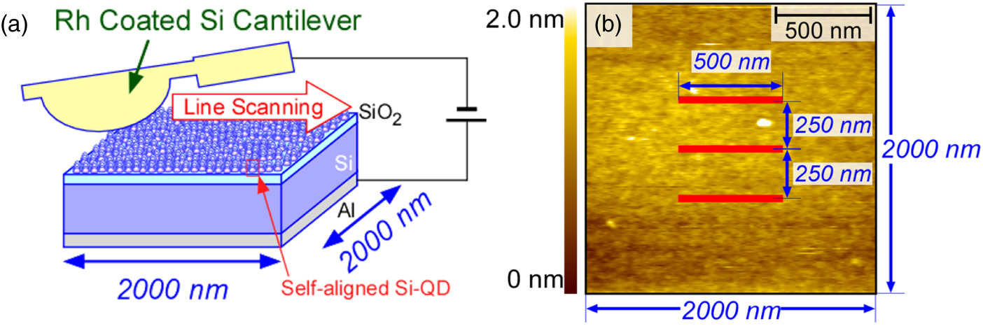
Charged states and charge retention characteristics of the self-aligned Si-QDs were carried out using a conductive Rh-coated Si cantilever at room temperature. Here, the radius of the tip apex of the cantilever and its spring constant was ∼10 nm and 1.7 N m−1, respectively. For charge injection into the QDs, the sample surface was electrically biased by the conductive Rh tip with a contact mode as scanning a line and space pattern changing the bias voltages as shown in Fig. 1(a). Here, the line width and spacing are 500 nm and 250 nm, respectively [Fig. 1(b)]. During the line scan, considering the tip radius and an areal dot density, the tip was simultaneously contacted to 2 dots. Before and after the electron injection, the topographic and corresponding surface potential images were simultaneously taken with a non-contact Kelvin-probe mode.

Fig. 1. (Color online) Schematic illustration of experimental procedure for surface potential measurements in the ultrahigh-density self-aligned Si-QDs. (a) Bias application with Rh tip for the self-aligned Si-QDs (Contact, line scan), and (b) corresponding AFM topographic image of the self-aligned Si-QDs during bias application.
Download figure:
Standard image High-resolution image3. Results and discussion
Surface potential images of self-aligned Si-QDs formed on ∼3.8 nm thick SiO2/n-Si(100) before and after applied voltages are shown in Figs. 2(a) and 2(b), respectively. In the case of the before applied voltage to the sample surface, a uniform surface potential image was observed. When the AFM tip was biased at −1.0, −1.5, and −2.0 V with respect to the sample surface, decreases in the surface potential at the scanned lines at each bias voltage were clearly observed. The decreases in the surface potential are associated with the electron injection from the Rh tip into Si-QDs and electron storage in the dots. From a cross-sectional potential profile along the dashed line from A to A' in Fig. 2(b), it is confirmed that changes in the surface potential depend on the applied tip bias, as shown in Fig. 2(c). Here, an average FWHM for the downward peaks in each cross-sectional potential in Fig. 2(c) is ∼107 nm, which corresponds to the diameter of the effective Rh tip electrode considering the spread of the electric field. In order to clarify the origin of the changes, the changes (ΔV) of the surface potential are plotted as a function of the applied bias, as presented in Fig. 3. Here, error bars in this figure are extracted from noise components in each cross-sectional potential profile. It is interesting to note that ΔV clearly indicates a stepwise shape, which could be owing to the discrete energy levels of Si-QDs. The following calculation makes it clear whether the origin is the discrete energy levels or not. Figure 4(a) shows a schematic diagram of the self-aligned Si-QDs based on the observed shape by HRTEM (Ref. 29). Figures 4(b) and 4(c) show simple equivalent circuit models for the self-aligned Si-QDs with different charged states. The models were modified from a model proposed in Refs. 26 and 27. Here, for simplicity, it is assumed that Si-QDs have a cylindrical structure with a radius (rhor.) and a thickness of rver.. In the actual case, the Si-QD has a hemispherical shape with an average height of ∼1.4 nm. The value is evaluated from a height distribution of Si-QDs by the lognormal distribution function in Ref. 31. This means a diameter (2 × rhor.) of the Si-QDs is 2.8 nm. Therefore, in our model, the value of 1.4 nm was used for both rhor. and rver.. Also, no Ge content in the lower Si-QD was assumed. Furthermore, it is assumed that the injected electron is located at the center of Si-QDs, reflecting the quantum confinement effects. In Fig. 4(b), an electron is injected in the upper dot and no electron is injected in the lower dot. In this case, a change (ΔVupper) of the surface potential can be given by ΔVupper = Δq/CB. Here, Δq and CB are the injected charge and capacitance with series capacitances between the center of the upper dot and the Si substrate, respectively. CB is given by CB = (εox
πr2)/tox. Here, εox and tox are dielectric constant of SiO2 and an equivalent oxide thickness (EOT) relating to the Si-QD/SiO2/Si-QD/SiO2/Si stack as shown in Fig. 4(b). According to the HRTEM image (Ref. 29), in Fig. 4(a), the bottom oxide thickness (tox1) and intermediate oxide thickness (tox2) are ∼3.8 nm and ∼1.0 nm, respectively. Furthermore, the thickness of the upper and lower QD is ∼1.4 nm, so the distance between the center of the upper QD and the interface of the SiO2/Si substrate is tox1 + rver. + tox2 + (rver./2) = ∼3.8 nm + ∼1.4 nm + ∼1.0 nm + (∼1.4 nm/2)  6.9 nm. On the other hand, the dielectric constant of Si and SiO2 are 11.9 and 3.9, respectively, so the thickness of Si-QD with the dielectric constant taken into account is thinner than the thickness of the actual structure. Therefore, tox is tox1 + (εox/ εSi)rver + tox2 + (εox/ εSi) (rver/2)
  5.5 nm. Furthermore, in the above-referenced formula, the series resistance CB is calculated by ∼9.0 aF. In Fig. 4(c), an electron is injected in the lower dot and no electron is injected in the upper dot. In this case, the change (ΔVlower) of the surface potential can be given by ΔVlower = Δq/C'B. Here, C'B is a capacitance with series capacitances between the center of the lower dot and the Si substrate. C'B is given by C'B = (εox
πr2)/t'ox. t'ox is EOT relating to the Si-QD/SiO2/Si stacks as shown in Fig. 4(c). As previously noted, the distance between the center of the lower QD and the interface of the SiO2/Si substrate is tox1 + (rver/2)
5.5 nm. Furthermore, in the above-referenced formula, the series resistance CB is calculated by ∼9.0 aF. In Fig. 4(c), an electron is injected in the lower dot and no electron is injected in the upper dot. In this case, the change (ΔVlower) of the surface potential can be given by ΔVlower = Δq/C'B. Here, C'B is a capacitance with series capacitances between the center of the lower dot and the Si substrate. C'B is given by C'B = (εox
πr2)/t'ox. t'ox is EOT relating to the Si-QD/SiO2/Si stacks as shown in Fig. 4(c). As previously noted, the distance between the center of the lower QD and the interface of the SiO2/Si substrate is tox1 + (rver/2)  4.5 nm. On the other hand, t'ox is tox1 + (εox/ εSi)(rver/2)
  4.0 nm, which is thinner than the thickness in the actual structure. In addition, plugging in the value of t'ox in the expression, the series resistance C'B is ∼12.2 aF. When a few electrons are simultaneously injected into the upper and lower dots, the change (ΔVtotal) of the surface potential can be given by ΔVtotal = ΔVupper + ΔVlower. According to the model, in the case of electron injection to the lower dot, ΔVtotal is −13 mV indicated by a red line in Fig. 3. It is found that the calculated ΔV value almost corresponds to the experimental results for the applied tip voltages from −0.1 to −0.55 V. In the applied voltages from −0.6 to −1.3 V, the observed ΔV values are in good agreement with the calculated result for two-electron injections in the upper and lower dots. In addition, in the range from −1.4 to −1.8 V, the experimental results are in good agreement with the calculated values that one electron is retained in the upper dot and two electrons are held in the lower dot. These agreements strongly indicate the stepwise ΔV as shown in Fig. 3 is attributable to the limited number of the stored electrons due to the discrete energy levels in Si-QDs.

Fig. 2. (Color online) A typical surface potential images taken (a) before, and (b) just after applied tip biases at −1.0, −1.5, and −2.0 V, and (c) corresponding cross-sectional potential profile along the line A–A' shown in (b).
Download figure:
Standard image High-resolution image
Fig. 3. (Color online) Change in surface potential evaluated by the surface potential as a function of tip bias.
Download figure:
Standard image High-resolution image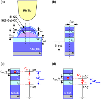
Fig. 4. (Color online) (a) A schematic diagram of the self-aligned Si-QD and (b) an equivalent cylindrical structure. (c) A corresponding circuit model to calculate the surface potential change due to electrons stored in the upper Si-QD and (d) in the lower Si-QD.
Download figure:
Standard image High-resolution imageTo investigate the temporal stability of the stored electrons in the self-aligned Si-QDs, we measured cross-sectional potential profiles along horizontal and vertical directions indicating white lines in insets in Figs. 5(a) and 5(b) passing times in 10 s, 30, 60, 90, and 120 min after the applied tip biases, as shown in Figs. 5(a) and 5(b). In Fig. 5(a), ΔV for each applied bias clearly decreases with time under non-contact Kelvin-probe mode. Also, the decrease in ΔV was observed in Fig. 5(b). We also confirmed that, for the case of the Si-QDs (single layer) with an areal density as low as ∼109 cm−2 formed on ∼3.8 nm thick SiO2/n-Si(100), no significant time dependence of ΔV was observed over ∼120 min, which could be attributed to stable storage of the electron into the Si-QDs (not shown). Therefore, the decreases in ΔV are surely owing to changes in the charged state in the self-aligned Si-QDs. In order to be more evident of the time dependence, the ΔV values at −0.5, −1.0, and −1.5 V are plotted as a function of the time, as shown in Fig. 6. When the electron was charged at −0.5 V, which means the electron is injected to the lower dot as discussed in Fig. 3, ΔV of −13 mV is stable until 120 min. On the other hand, in the case of −1.0 and −1.5 V, the steps are observed at ∼20 min and ∼40 min, respectively. After charging at −1.0 V until 20 min, ΔV is −31 mV, which is attributable to one electron being stored in the upper dot and another electron being stored in the lower dot as discussed in Fig. 3. Then, more than 20 min, ΔV becomes −26 mV, indicating that the two electrons are stored in the lower dot. This means that the electron stored in the upper dot moves to the lower dot due to the tunneling through the ultra-thin oxide layer. With an increase in the applied tip bias up to −1.5 V, ΔV is −44 mV, which is stable until ∼40 min. Then, ΔV becomes ∼39 mV for more than 40 min. These behaviors can be explained by the following. In less than 40 min, one electron is stored in the upper dot and two electrons are stored in the lower dot. At around 40 min, the electron stored in the upper dot moves to the lower dots. As a result, three electrons are stored in the lower dot. These results can be explained that the conduction band minimum (C.B.M.) of the lower SiGe-QD is expected to be slightly lower than that of the upper Si-QD and energy relaxation due to Coulomb force between the charged electrons and the donor ions in the n-Si substrate (that is to say shortening lines of electric force). Here, it should be noted that considering our sample fabrication process, the Ge content of the lower QD could be significantly low. Thus, C.B.M. of the upper- and lower QD can be regarded as almost the same. These results suggest that the number of electrons can be controlled by the bias voltage applied to the dots. On the other hand, at the same time, these results suggest that the stored electrons in the upper dot are not stable. In order to stabilize the stored electrons, further study is mandatory.
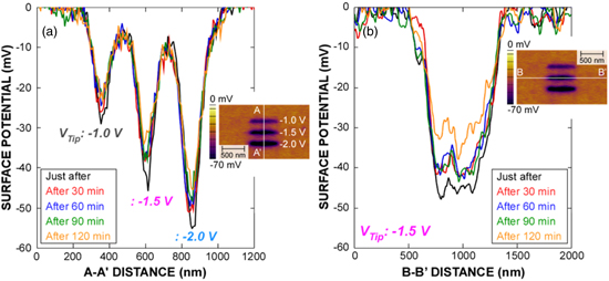
Fig. 5. (Color online) Cross-sectional potential profiles along (a) the line A–A', and (b) the line B–B', shown in the inset, taken just after, in 30, 60, 90, and 120 min applied tip biases at −1.0, −1.5, and −2.0 V.
Download figure:
Standard image High-resolution image
Fig. 6. (Color online) Room temperature decay characteristics of surface potential changes taken after applying tip biases at 0.5, −1.0, and −1.5 V.
Download figure:
Standard image High-resolution image
4. Conclusions
In this study, we have characterized the electron charged states after the electron injections to the self-aligned Si-QDs structure with the areal density of ∼1013 cm−2 by the surface potential measurements using the AFM/Kelvin probe technique. We have succeeded to detect the change in the charged states in Si-QDs due to the quantum effect at room temperature even in Si-QDs formed on the SiO2 layer with the high density, not from one dot. It was also found that the charge states can be controlled by changing the voltage applied to Si-QDs. On the other hand, since the electrons are preferentially stored in the lower dots, it is clear that the stability of electrons in the upper dots is an issue. This is quite informative in the realization of quantum dot devices operating at room temperature.
Acknowledgments
This work was supported in part by Grant-in-Aid for Scientific Research (A) 19H00762 and 21H04559 of MEXT Japan, and the Cooperative Research Project Program of the Research Institute of Electrical Communication, Tohoku University.