

Abstract
GaAsN films with different N distributions have been grown using the atomic layer epitaxy method to evaluate the effects of N distribution on the electrical properties of GaAsN. Three films, which had the same N composition with different N distribution were fabricated by alternate stack of GaAsN 1 monolayer (ML) and GaAs (0, 3, 5) ML. According to the X-ray diffraction measurement, periodicity and small N interdiffusion between GaAs and GaAsN layers in grown GaAsN films were confirmed. Thus, N distribution in the films were successfully modified in the order of a few unit lattice. Contribution of each scattering mechanisms on carrier mobility and densities of scattering centers in grown GaAsN films were evaluated. Compared with the film with 0 ML of GaAs, the density of N induced scattering center decreased with insertion of GaAs 3 ML between GaAsN 1 ML. It again increased the film with insertion of GaAs 5 ML. These results suggest that controlling N distribution intentionally not only degraded but also improved the electrical properties of GaAsN films.
Export citation and abstract BibTeX RIS
1. Introduction
It is known that a multi-junction solar cell structure is promising for improving efficiency. The lattice constants and band gap energies of constituent semiconductor materials are important for stacking different kinds of p–n junctions monolithically.1,2) Conventional three-junction solar cell of InGaP/(In)GaAs/Ge structure3) still have a problem such that the band gap energies are quite different between GaAs and Ge cells. This induced the current mismatch problem and reduced the conversion efficiency. Then, a new absorbent layer between the GaAs and Ge is desired. Since (In)GaAsN with compositions of In 9% and N 3% is lattice-matched to GaAs and Ge cell, it is expected as materials for ultra-high-efficiency multi-junction solar cells with a conversion efficiency of more than 45%.4) At the same time, nitrogen-containing III–V alloys have attracted attention because a very small amount of nitrogen lowered the alloy's band gap markedly.5–8) However, the electrical properties of (In)GaAsN, such as carrier lifetime and mobility deteriorate significantly with the addition by even a small amount of N to GaAs.9,10) This deterioration is considered to be originated from N-related point defects and/or fluctuations in the distribution of N.11–15) Recently, it has been reported that the electrical properties of GaAsN films were improved by using a chemical beam epitaxy (CBE).16,17) This improvement might be understood by characteristics of the CBE method, which is sensitive to the morphological characteristics of the growing surface than other growth technique such as molecular beam epitaxy (MBE) and metal organic chemical vapor deposition.18,19) This suggests that controlling the structure and morphology of the growth surface are key issues to improve the electrical properties of GaAsN. Actually, N induced scattering centers for carriers could be reduced by controlling the surface during growth.18) This method might improve homogeneity of N distribution; however, it was difficult to observe N distribution in the GaAsN films.
Therefore, in this study, to investigate the influence of spatial distribution of N on the electrical properties of GaAsN films, we performed following experiments. At first, we tried to grow GaAsN thin films with different N spatial distribution and evaluated actual N distribution in the films. Then, we evaluated scattering mechanisms and density of scattering centers for carriers of the films. So far spatial distribution of N atoms in films has been controlled by δ-doping technique. In this method, radical N atoms were used as N source and were supplied by RF plasma source. During MBE growth of GaAs films, radical N was supplied on GaAs surfaces to make δ-doping layer, and δ-doped superlattices of N atoms between GaAs layers were fabricated.20–23) Due to high energy of RF plasma, N atoms incorporated into the GaAs matrix not only on the surface but also several inside layers. In other words, N atoms distributed several layers. Thus, above studies focused on electrical properties of superlattice structures with long periods (∼a few nm)20,21,23) or luminesce property from single δ-doping layer.22) To reveal effects of N distribution on electrical properties, it is necessary to control N distribution in order of few atomic layers.
Therefore, we focused on the atomic layer epitaxy (ALE) method24) as a growth method that can explicitly change the distribution of N atoms and obtain a growth layer in atomic layer units. ALE technique can control the growing surface with an accuracy of a single atomic layer by the self-limiting mechanism (SLM).25,26) We have already found the optimal gas flow sequence and proposed the growth model of GaAsN.26,27) Then, we applied the ALE method to grow GaAsN films with different N distribution by combining sequences for GaAsN and GaAs atomic layers. Scattering mechanisms and their densities in grown GaAsN films were evaluated by temperature dependence of carrier mobility. Growth processes of GaAsN films with different N distribution and their temperature dependence of hole mobility are already reported in the previous abstract,28) detailed analysis of the N distribution in the films using X-ray diffraction (XRD), and a discussion of the origins for each scattering center were added in this paper.
2. Experimental procedure
GaAsN thin films were grown on semi-insulating GaAs (001) substrates using the ALE method. To control N distribution in GaAsN films, two gas flow sequences, as shown in Fig. 1, were used in combination. In ideal condition, one cycle of each sequence could grow one monolayer (ML) of GaAsN and GaAs. M and N cycles of sequence A and B were supplied alternatively as a set, and the set were repeated L times to grow GaAsN film. The films grown by these sequences were called (M:N). If the films are grown ideally as designed, (M:N) film has a superlattice structure with (M + N) times period along growth direction, and total thickness of the film is (M + N)L [ML]. For example, (1:3) means the superlattice structure repeating 1 ML of GaAsN and 3 ML of GaAs as shown Fig. 2(b) and has four times period along growth direction. (1:3) and (1:5) films were prepared in this study using this procedure. For comparison, we also grew GaAsN film using only sequence A, which was conventional GaAsN film grown by ALE and was called as (1:0). Repeating number L for (1:0), (1:3) and (1:5) were 720, 180, and 120, respectively. Thus, total thickness for all films were 720 ML (204 nm). To equalize average N composition in these films, N composition per ML grown by sequence A was controlled. N composition per 1 ML was controlled by changing N duration per cycle. Durations of N for (1:0), (1:3), and (1:5) were 0.53, 2.48, and 5.39 s, respectively. Schematic structures of grown GaAsN films were summarized in Fig. 2. Schematic structures of grown GaAsN films were summarized in Fig. 2. (1:5) has the most inhomogeneous distribution of N. GaAsN precursor gases were (CH3)3Ga (TMGa), H3N2CH3 (MMHy), and [N(CH3)2]3As (TDMAAs). Hydrogen was used as both the carrier and the purge gas. Details of our growth facilities were described in our previous papers.21) Flow rates of the source gases for N, As, and Ga were fixed as 9.60, 4.80, and 4.80, respectively. Durations for the As and Ga sources were fixed at 6.0 and 10 s. All films were grown at 480 °C under 12.6 Torr.
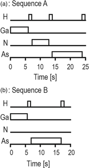
Fig. 1. Gas sequences for monolayer growth for (a) GaAsN and (b) GaAs. N precursor gas supplied at 0.53–5.39 s. Ga and As precursor gases supplied at 6 and 10 s, respectively.
Download figure:
Standard image High-resolution image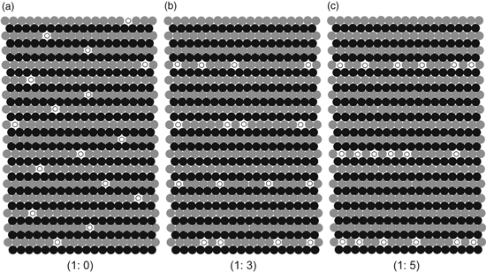
Fig. 2. Schematic models of GaAsN films grown in this study. Figure (a), (b) and (c) show (1:0), (1:3) and (1:5). The black, gray and white circles indicate Ga, As and N atoms, respectively.
Download figure:
Standard image High-resolution imageN composition and superlattice structures of the films were evaluated XRD. All films grown in this study showed p-type conductivity. Temperature dependence of carrier mobility of the films at 80–300 K was evaluated by the Hall-effect measurement by the van der pauw method. Four Ag electrode dots were evaporated on the film surfaces. Distance between adjacent electrodes was 3.5 mm. The electrodes were annealed at 400 °C for 30 min in N2 atmosphere to form an ohmic contact.
3. Results and discussion
XRD patterns around (004) diffraction for the GaAsN thin films with different N distributions are shown in Fig. 3(a). For comparison, simulation curve for the (1:5) film is also indicated in the figure. Peak positions of GaAsN (004) for all films are almost the same and clear thickness interference fringes were observed. Peak position, width, and spacing of fringe peaks of (1:5) are good agreement with the simulation. These indicated good crystallinity and the average of N composition is the same (∼0.4%). Thickness of the films calculated from spacing of the fringe peaks and XRD simulation was 229 nm, which was slightly larger than the designed value. This means SLM condition was not perfect and actual growth thickness per cycle in this study was 1.1 ML.

Fig. 3. XRD patterns of GaAsN thin films with different N distributions. (a) and (b) show around GaAsN (004) diffraction peak and superlattice diffraction peak, respectively.
Download figure:
Standard image High-resolution imageOn the lower side of (004) diffraction, as shown in Fig. 3(b), weak peaks were observed at around 60° and 58° for the (1:5) and (1:3) films. To analyze N distribution in the films, XRD simulation was performed and compared with experimental results. Experimental result of (1:5) and simulation result are shown in Fig. 4. Here, to equalize peak positions of GaAsN (004) and 1st satellite peak, N composition in each film and periodicity along the growth direction were modified. Intensities were normalized by GaAsN (004) peaks. 1st and 2nd satellite peaks were observed in the simulation. However, only 1st satellite peak can be observed in the experimental result. This is because, the intensity of the 2nd peak is lower than background. The inset of Fig. 4 shows enlarged pattern around the 1st satellite peak. The peak in experimental results is lower and broader than simulation. The GaAsN 004 peak did not broaden as shown in Fig. 3, the broadening of the 1st satellite peak was not originated from crystal defects and thinner thickness but from and fluctuation of superlattice period. This could be understood by fluctuation of growth rate per cycle on the growing surface. In other words, more than 1 ML films were grown in some region per cycle. The estimated period is 6.6– 7.2. This is consisted with the actual growth rate per cycle (1.1 ML s−1) estimated from the film thickness. Although peak heights are different, the integrated intensities of both experimental and simulation data are almost the same. This suggests that diffusion of N atoms into GaAs layers are small. The same analysis was applied for (1:3), and summarized in Table I.

Fig. 4. Superlattice GaAsN diffraction peaks of experience data (upper) and simulation data (lower). The inset shows enlarge pattern around the 1st satellite peak.
Download figure:
Standard image High-resolution imageTable I. Superlattice structure periods estimated by simulation fitting.
| (GaAsN:GaAs) | Estimated superlattice structure period |
|---|---|
| (1:3) | 4.4–4.8 |
| (1:5) | 6.6–7.2 |
Here, we would like to make small conclusion for growth. Although superlattice periods were slightly fluctuated, we have successfully grown GaAsN thin films with different N distribution In addition, we would like to note that the films grown in this study were different from the δ-doped ones discussed in the literature20–23) in points of small interdiffusion of N atoms and shorter period of superlattice. Thus, the effects of N distribution, in other words the effects of spacing of adjacent N atoms in GaAsN layers, on electrical properties could be evaluated using these films instead of superlattice structures with long period.
Figure 5 shows temperature dependence of mobility of GaAsN thin films. Less than 100 K, the values of (1:3) and (1:0) are almost the same. Above 100 K, (1:3) is larger than (1:0). In all measurement region, mobility of (1:5) is the lowest. Peak temperatures for (1:0) and (1:3) are 220 K, but that for (1:5) is 250 K. These suggest that the contribution of each scattering mechanism for grown films are different. Then, the contribution of scattering process on carrier mobility is separated by parameter fitting. Ionized impurity scattering ( ), alloy scattering (
 ), and phonon scattering (
 ) were considered. By assuming Mattiessen's rule, the total whole mobility (
 ) is given by the following equation
It is noted that alloy scattering mentioned here includes N induced scattering. Because alloy scattering and N induced scattering have the same temperature dependence. Due to low N composition, we assumed phonon scattering of the films are the same of GaAs. According to the literature, mobilities limited by ionized impurity scattering and alloy scattering can be written as  and
and  respectively.29) Here,
  and
and  were fitting parameters, and inverse numbers of them (
 and
and  ) are proportional to density of scattering centers.
  is correspond to density of ionized impurities. According to the previous reports,30) in p-type GaAsN, N induced scattering had the same temperature dependence with alloy scattering. Therefore, the
  represents the sum of alloy scattering and the N induced scattering. Figure 6. shows experimental and fitting results for (1:5). The three scattering mechanisms reproduce the experimental results well.

Fig. 5. Temperature dependence of mobility of GaAsN thin films.
Download figure:
Standard image High-resolution image
Fig. 6. Experimental and calculated hole mobilities for GaAsN (1:5) as a function of temperature. Filled triangles are experimental value  The solid lines are the total hole mobility
  acoustic phonon (
 ), alloy (
 ), and ionized impurity (
 ) scattering.
Download figure:
Standard image High-resolution imageThe relationship between the values of  and carrier density are shown in Fig. 7(a).
  for (1:0) and (1:3) are almost the same, and only that of (1:5) has higher value. Although
  increases with increasing carrier density, the relationship is not linear. This could be understood by compensation of donors and acceptors. The origins of carrier are residual impurities such as C and H from source gases. Especially, C and H comes from the N precursor.24) Complex defects including N and H atoms have been predicted as both donor and acceptor. In addition, it was reported that GaAsN film grown by CBE using the same precursors of this study were compensated. Thus, we concluded that the films were compensated and the (1:5) film has the highest concentration of residual impurities. Take into account the N duration and growth sequence for each film, total times of the N precursor flow for (1:0), (1:3) and (1:5) during film growth were 381.6, 446.4, and 646.8 s, respectively. This might be the origin of the high impurity concentration of (1:5).
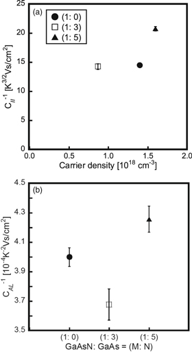
Fig. 7. Regression coefficients of grown GaAsN films. (a) and (b) are inverse of regression coefficients of ionized impurity ( ) and alloy (
 ) scattering, respectively.
Download figure:
Standard image High-resolution imageThe values of  are shown in Fig. 7(b). Although N composition of all films are the same,
  of (1:3), (1:0), and (1:5) increases in this order. These indicate that density of N induced scattering center are different. The (1:5) film, which has the most inhomogeneous N distribution, has the highest value. The (1:3) film also has inhomogeneous N distribution compared with (1:0), however the value is less than (1:0). To discuss the effect of N distribution, we consider the spacing of N atoms in the GaAsN film. We simulated positions of N atoms in the films and calculate the spacing of adjacent N atoms. The histograms of the spacing were shown in Fig. 8. In the simulation, each layer was consisted of 60 × 60 unit cells and 120 layers were stacked. 0.4%, 1.2% and 2.4% of N were located in N including layer for (1:0), (1:3) and (1:5) films, respectively. Here, we assumed that N atoms did not diffuse other layers, and were located randomly in a single atomic layer. According to the XRD results, amount of N interdiffusion was not so large.

Fig. 8. The histograms of adjacent N spacing calculated from the simulation. In the simulation, N atoms were located randomly in the layer. each layer was consisted of 60 × 60 unit cells and 120 layers were stacked. 0.4%, 1.2% and 2.4% of N were located in N including layer for (1:0), (1:3) and (1:5) films, respectively.
Download figure:
Standard image High-resolution image
In the films of (1:3) and (1:5), some spacing values, which were observed in the (1:0) film, disappeared as indicated by arrows. These values are the distance between N atoms in adjacent layers along [001] direction. This is due to intermittent insertion of GaAsN layers in the case of (1:3) and (1:5). On the other hand, the value of the nearest neighbor N increasing in monotonically increase with increasing of N composition in the single GaAsN layer. The one of possible explanation to explain nonlinear change of N induced scattering in the films is as follows. N induced scattering center is related to the N atom pair with close position. Some of them are disappeared by intermitted insertion of N, while the atoms at nearest neighbor position increases. Although, more detail results should be required, the results suggest that controlling N distribution intentionally not only degraded but also improved the electrical properties of GaAsN films.
4. Conclusions
GaAsN films with different N distributions have been grown using the ALE method to evaluate the effects of N distribution on the electrical properties of GaAsN. Three films, which had the same N composition with different N distribution were fabricated by alternate stack of GaAsN 1 ML and GaAs (0, 3, 5) ML. According to the XRD measurement, periodicity and small N interdiffusion between GaAs and GaAsN layers in grown GaAsN films were confirmed. Thus, N distribution in the films were successfully modified in the order of a few unit lattice. Contribution of each scattering mechanisms on carrier mobility and densities of scattering centers in grown GaAsN films were evaluated. Compared with the film with 0 ML of GaAs, the density of N induced scattering center decreased with insertion of GaAs 3 ML between GaAsN 1 ML. It again increased the film with insertion of GaAs 5 ML. These results suggest that controlling N distribution intentionally not only degraded but also improved the electrical properties of GaAsN films.
Acknowledgments
A part of this study was supported by JSPS KAKENHI Grant No. 16K17515.