
An Improved Voltage Clamp Circuit Suitable for Accurate Measurement of the Conduction Loss of Power Electronic Devices

State Key Laboratory of Alternate Electrical Power System with Renewable Energy Sources, North China Electric Power University, Beijing 102206, China
*
Author to whom correspondence should be addressed.
Sensors 2021, 21(13), 4285; https://doi.org/10.3390/s21134285
Submission received: 3 June 2021
/
Revised: 17 June 2021
/
Accepted: 21 June 2021
/
Published: 23 June 2021
(This article belongs to the Section Electronic Sensors)
Abstract
:Power electronic devices are essential components of high-capacity industrial converters. Accurate assessment of their power loss, including switching loss and conduction loss, is essential to improving electrothermal stability. To accurately calculate the conduction loss, a drain–source voltage clamp circuit is required to measure the on-state voltage. In this paper, the conventional drain–source voltage clamp circuit based on a transistor is comprehensively investigated by theoretical analysis, simulations, and experiments. It is demonstrated that the anti-parallel diodes and the gate-shunt capacitance of the conventional drain–source voltage clamp circuit have adverse impacts on the accuracy and security of the conduction loss measurement. Based on the above analysis, an improved drain–source voltage clamp circuit, derived from the conventional drain–source voltage clamp circuit, is proposed to solve the above problems. The operational advantages, physical structure, and design guidelines of the improved circuit are fully presented. In addition, to evaluate the influence of component parameters on circuit performance, this article comprehensively extracts three electrical quantities as judgment indicators. Based on the working mechanism of the improved circuit and the indicators mentioned above, general mathematical analysis and derivation are carried out to give guidelines for component selection. Finally, extensive experiments and detailed analyses are presented to validate the effectiveness of the proposed drain–source voltage clamp circuit. Compared with the conventional drain–source voltage clamp circuit, the improved drain–source voltage clamp circuit has higher measurement accuracy and working security when measuring conduction loss, and the proposed component selection method is verified to be reasonable and effective for better utilizing the clamp circuit.
1. Introduction
High-voltage, large-capacity power electronic conversion equipment dramatically improves the transmission capacity of the flexible AC/DC grid as well as the electric traction control ability [1]. As the voltage withstand ability and switching frequency of power semiconductor devices continue to increase, and the volume continues to decrease, power electronic converters have higher efficiency and power density [2,3,4]. However, converters face reliability challenges. The overheating failure of the internal power electronic devices is one of the main reasons for damage to the converter [5,6,7], and most heat comes from the power loss of power semiconductor devices. Imprecise power loss measurement will lead to the wrong design of the thermal management system (TMS), which will affect the reliability and cause premature failure of the equipment [8,9]. Accurately obtaining the power loss of the device is a crucial prerequisite for determining the thermal solution, which will affect the efficiency, cost, and power density of the entire system.
Common methods for obtaining power loss are calorimetry [10,11], building a physical model [12,13], establishing a loss look-up table or fitting power loss as a function [14,15], and directly integrating the product of the square of the on-state current root mean square and the on-state resistance [16]. However, the above methods often introduce significant errors due to model or measurement problems.
At present, an accurate way to calculate power loss, including switching loss and conduction loss, is to measure the on-state drain–source voltage (vds_on) across the device and the current (id) flowing through the device and then integrate their product. However, when calculating the conduction loss, it is difficult to measure the on-state voltage accurately. It is directly related to the operating characteristics of the power semiconductor device that frequently converts between the on state and the off state. The off-state drain–source voltage (vds_off) can reach hundreds or thousands of volts, while the on-state voltage vds_on is only a few volts [17], making it challenging to select a suitable oscilloscope range. An excessive range will lead to a significant error in the on-state voltage measurement, and more seriously, the measurement result may be negative due to the influence of noise. If the oscilloscope range is set too small, the “oscilloscope saturation” phenomenon will be seen [18].
The drain–source voltage clamp circuit (DVCC) is frequently used to measure the on-state voltage vds_on by clamping the off-state voltage of the device under test (DUT) to a lower value. In existing research, six types of DVCCs have been proposed for the measurement of vds_on. The DVCC proposed in [19,20] clamps the off-state voltage of the DUT by using the high-voltage breakdown characteristics of the Zener diode. It is simple to implement. However, its measurement error due to the leakage current of the Zener diode and its measurement delay due to the resistance–capacitance (RC) loop limit its further application. Gelagaev [18] analyzed the DVCC based on a current mirror in detail, and this circuit solved the problem of measurement delay. However, it has been shown that since the output currents on both sides of the current mirror cannot be entirely consistent, the current flowing through the diodes on both sides may be different, which may cause measurement errors. Furthermore, in [21], a DVCC based on one diode is described. The forward voltage of its diode is affected by temperature and current, leading to cumbersome corrections for vds_on. This problem was resolved in [22,23]. The DVCC proposed in [22,23] introduced two diodes and a proportional amplifier circuit to improve measurement accuracy. However, due to the difference in the physical positions and forward current of the two diodes, it is difficult to ensure that the voltage drop of the two diodes is equal, which may lead to inaccurate results. Yu et al. [24] presented an innovative design for the DVCC with improved real-time measurement accuracy. Guacci et al. described a DVCC in [25], which can accurately correct the voltage offset caused by the diode voltage drop and has a higher measurement accuracy. Both of these circuits in [24,25] introduce operational amplifiers, which increases the complexity of the course. A DVCC integrated with a half-bridge circuit was employed in [26] for device evaluation in the hard-switching test and the soft-switching conditions. However, this DVCC ignores the influence of diode leakage current on the on-state voltage measurement, and there may be measurement errors. The DVCC based on the transistor is analyzed in [27]. It avoids most of the problems mentioned earlier. However, the gate–source spike voltage due to the instantaneous high current of the transistor gate resistance may damage the DVCC itself. Additionally, the purpose of designing this circuit is to measure on-state resistance Rds_on, and it is not suitable for conduction loss measurement.
In summary, these existing DVCCs, in terms of measurement accuracy, work complexity, and design aim, cannot be used for conduction loss (Ploss_on) measurement of power semiconductor devices. Therefore, this paper concerns the drawbacks of the conventional DVCC based on the transistor (hereinafter referred to as “conventional DVCC”) and proposes an improved DVCC (hereinafter referred to as “improved DVCC”) architecture suitable for the Ploss_on measurement. The new circuit is derived from the conventional DVCC. The remainder of this paper is organized as follows. In Section 2, the circuit structure, work principle, and drawbacks of the conventional DVCC are analyzed in detail. Then, the schematic and the advantages of the improved DVCC are presented. Furthermore, the influence of the components’ parameters on the circuit performance of the improved DVCC is analyzed in Section 3. Here, component selection guidelines are also given. In Section 4, the measurement accuracy and work security improvement of the improved DVCC are verified through simulated and experimental comparisons with the conventional DVCC. Simultaneously, the effectiveness of the selection theory is also investigated and proven. Finally, Section 5 concludes this paper.
2. Design of the Improved DVCC
Compared with the existing DVCCs, which are mainly applied to the on-state resistance measurement of the DUT, more problems need to be considered when designing a DVCC suitable for conduction loss measurement. After the DUT is turned on, it will go through two typical states, enter the oscillation state (on-oscillation state), and gradually reach steady state (on-steady state). The measurement results of these existing DVCCs can well reflect the on-state voltage vds_on_ste when the DUT is in the on-steady state. However, when measuring the conduction loss, in addition to the above-mentioned on-steady state voltage, the DVCC must be able to accurately measure the on-state voltage vds_on_osc when the DUT is in the on-oscillation state. Any error at any stage will cause errors in the calculation of the device conduction loss.
In addition, many common problems need to be avoided in both on-state resistance and conduction loss measurement. First of all, the DVCCs cannot have measurement delays. Once the voltage data lag or lead the current data, errors will occur in the loss integral calculation. Secondly, power electronic devices, such as diodes, metal–oxide–semiconductor field–effect transistors (MOSFET), etc., are often introduced into DVCCs to realize the voltage clamping function. Due to the faster switching speed and higher operating voltage of the DUT, it is easy to make these auxiliary devices out of safe working conditions. Therefore, when designing a DVCC, it is necessary to focus on the security of these auxiliary devices.
2.1. The Structure and Working Principle of the Conventional DVCC
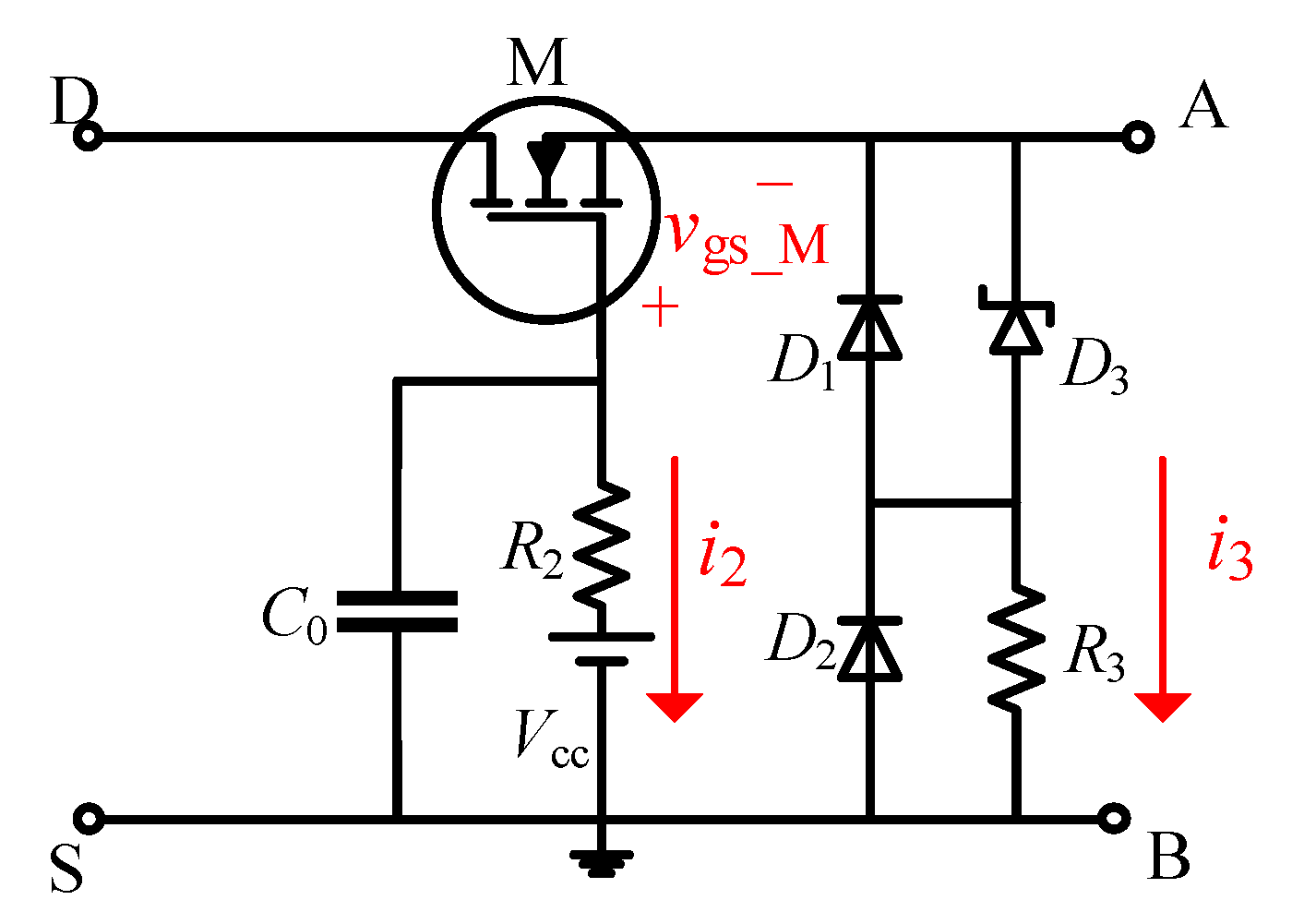
The schematic diagram of the conventional DVCC is shown in Figure 1. The auxiliary device MOSFET (M) is used to withstand the high off-state voltage of the DUT, thereby limiting the potential of the voltage measurement point A. The DC voltage supply Vcc and the gate resistor R2 are located at the gate of M, and together with the resistor R3, they control the turn-on and turn-off of M. The D and S terminals of the circuit are connected to the drain and source of the DUT, respectively, while the A and B terminals are used to measure output voltage (vout).
When the DUT is in the off-state, D3 is broken down, causing the current flowing through R3 to increase sharply. At this time, the source potential of M rises, and the gate-source voltage vgs_M decreases. When vgs_M is less than the threshold voltage Vth_M of M, M is turned off and shares most of the off-state voltage, limiting vout to a small voltage value. When the DUT is turned on, the source potential of M decreases, causing the vgs_M to become higher than Vth_M, bringing the M into conduction. As a result, vout is equal to vds_on.
2.2. Drawbacks of the Conventional DVCC
In view of the fact that the purpose of the conventional DVCC is to measure the on-state resistance, when it is applied to conduction loss measurement, there are some severe problems, which are further discussed in the following subsections.
2.2.1. Low Measurement Accuracy
To reduce the voltage negative overshoot between A and B when the DUT is turned on, the conventional DVCC connects the diodes D1 and D2 in reverse parallel between the measurement points A and B and utilizes their unidirectional conductivity characteristics to eliminate the voltage overshoot.
Assume that the forward voltage drops of diodes are VD1 and VD2, respectively. During the on-oscillation state, if vds_on_osc is greater than −(VD1 + VD2), D1 and D2 are reversely cut off. Therefore, vout = vds_on_osc. Once vds_on_osc is less than −(VD1 + VD2), D1 and D2 will immediately switch to the forward conduction state, and the output voltage will remain unchanged at −(VD1 + VD2), resulting in vout ≠ vds_on. The two diodes limit the negative voltage overshoot and do not affect the on-state resistance measurement. However, when measuring the conduction loss, the loss during oscillation cannot be ignored [28]. The conventional DVCC cannot measure vds_on_osc accurately nor can it accurately measure the conduction loss.
2.2.2. Low Working Security
To reduce the current flowing through the DC voltage supply (Vcc) and ensure the safety of Vcc, the conventional DVCC shown in Figure 1 has a capacitor C0 connected in parallel to the gate of M [22]. However, the existence of C0 seriously affects the work security of auxiliary device M. When the DUT is turned off, the drain–source voltage vds and the current on R3 increases sharply, which will cause an instantaneous negative overshoot Vgs_M(max) at the gate–source of M. If Vgs_M(max) exceeds the gate−source voltage withstand limit of M (Vgs_limit), M will be burned. If negative overshoot Vgs_M(max) occurs at time t0, the gate−source voltage vgs_M of M will be a negative value in the time interval [t0 − Δt, t0 + Δt]. According to Figure 1, it can be known from KVL that during this period, vgs_M can be written as in Equation (1), and Vgs_M(max) = vgs_M(t0):
where VD3 is the breakdown voltage of Zener diode D3; i2 and i3 are the current flowing through R2 and R3, respectively.
Adding C0 to the gate of M will reduce i2(t0), which can protect Vcc. However, since Vgs_M(max) is negative, the decrease in i2(t0) will cause the absolute value of Vgs_M(max) to increase significantly, which will endanger the safety of the MOSFET. In contrast, the impulse current withstand capability of the widely used DC voltage supply can reach several amperes or tens of amperes. Even without C0, i2(t0) is not enough to cause harm to Vcc. Therefore, the benefit of C0 is far less than the harm it causes.
2.3. Proposal of the Improved DVCC
The schematic of the improved DVCC for conduction loss measurement is described in Figure 2. By conducting two changes in the structure of the conventional DVCC, the problems existing in the conventional DVCC are solved.
Firstly, to accurately measure vds_on_osc of the DUT, the improved DVCC removes anti-parallel diodes (i.e., D1 and D2 in Figure 1) from the output voltage measurement point. Under this arrangement, the on-state voltage of the two stages, on-steady state and on-oscillation state, both have high measurement accuracy. Furthermore, the calculation error of conduction loss is limited to a small value.
In addition, considering the harmfulness of C0 to the core device M, another improvement is to remove the gate-shunt capacitance (i.e., C0 in Figure 1). This measure dramatically improves the operating environment of M. In addition, there is no need to worry about the safety of Vcc. For typical DC sources, their impulse current tolerance often reaches several amps or tens of amps, while the maximum current flowing through Vcc is usually hundreds of milliamps. Therefore, the work safety of Vcc will not be threatened.
3. Component Selection
In Section 2, the pros of the improved DVCC and the cons of conventional DVCC were highlighted. In this section, the influence of component parameters on the performance of the improved DVCC is analyzed in detail. Furthermore, guidelines for component selection are given to utilize the improved circuit better.
3.1. Evaluation Indicators
Theoretically, there are three conditions that the circuit must meet to perform the functions of clamping and measuring normally, as listed below.
- Ensure the security of core MOSFET (M);
- M should be in the proper working state when the DUT is in the on-state;
- M should be in the proper working state when the DUT is in the off-state.
Considering the above three restrictions, this article comprehensively extracts three electrical quantities as the judgment indicators of the circuit performance to guide component selection:
- Gate−source voltage negative overshoot (Vgs_M(max)) of M, which is denoted as EI1. As indicated in Section 2, it is necessary to avoid Vgs_M(max) exceeding the gate–source tolerance of core M. Therefore, the low EI1 value is of greater significance for improving the security of M.
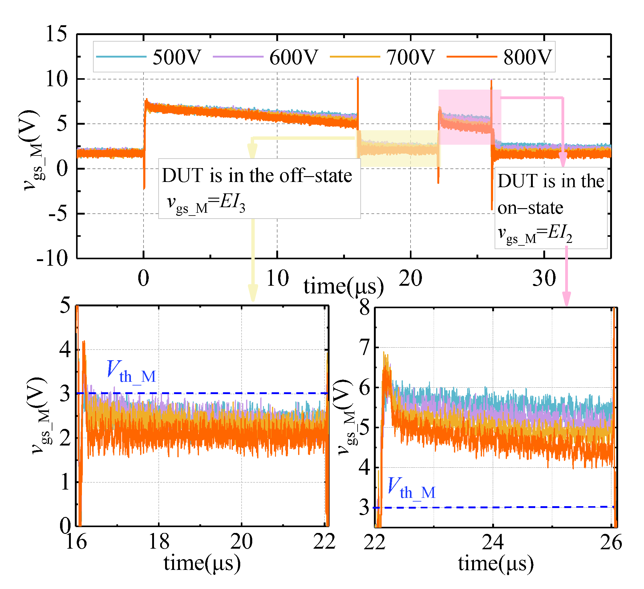
- Gate−source voltage of M (vgs_M(on)) when the DUT is in the on-state, which is denoted as EI2. If the DUT is in the on-state, M should also be in the on-state to satisfy vout = vds_on. Therefore, the second evaluation indicator should meet EI2 > Vth_M.
- Gate−source voltage of M (vgs_M(off)) when the DUT is in the off-state, which is denoted as EI3. When the DUT is in the off-state, the working state of M should also be consistent with the DUT to withstand high off-voltage and reduce the potential of the measurement point A. Under this condition, EI3 should be less than Vth_M, so that M can be turned off reliably [29].
3.2. Selection of MOSFET
Since the parameters of M are closely related to the safe operation of the entire circuit, criteria for selecting the subject are proposed based on the working principle of the improved DVCC.
As stated before, with the transitions of DUT from the on-state to the off-state, M also changes its state rapidly so as to prevent the continuous increase of the source current of M and prevent EI1 from being too large. Similarly, when the DUT changes from the off-state to the on-state, M needs to be turned on immediately to avoid measurement delay. Therefore, it is recommended that the switching speed of M be consistent with or faster than DUT, which is the first criterion for the selection of M.
In addition, since the improved DVCC utilizes the high blocking voltage characteristic of M to exercise the clamping function, during the off-state of the DUT, the drain–source withstand voltage of M is almost the same as that of the DUT. To increase the operational reliability of M, it is advised that the blocking voltage level of M is consistent with or higher than the DUT, which is considered the second criterion.
3.3. Selection of DC Voltage Supply Vcc and Zener Diode Breakdown Voltage VD3
3.3.1. Selection Principle of VD3
Since Zener diode D3 is in the gate−source loop of M, EI1 is one of the vital evaluation indicators for selecting VD3. The influence of VD3 on the work security of M is analyzed in this subsection.
According to Figure 2, the gate−source negative overshoot of M can be expressed as follows:
where I2 and I3 are the currents flowing through R2 and R3 at time t0, respectively.
According to Equation (2), VD3 increases, and the absolute value of EI1 increases accordingly. Based on the interpretation content of the first evaluation indicator, for high security of M, VD3 should be as small as possible.
3.3.2. Voltage Constraint for Effective Work
The DC voltage supply Vcc and the Zener diode D3 jointly control the turn-on and turn-off of M to make it follow the steps of the state change of DUT. Therefore, it can be seen that the values of vgs_M(on) and vgs_M(off) are closely related to Vcc and VD3. Based on the supplementary content when the second and third evaluation indicators are proposed, it can be estimated that Vcc and VD3 have a mutually restrictive relationship. In this paper, this specific constraint is called the “voltage constraint for effective work (VCEW)” and is further discussed in the subsequent sections.
When the DUT is in the on-state, EI2 can be expressed as in the equation below:
where i2_on is the current flowing through the resistor R2 when the DUT is in the on-state.
Since M is also in the on-state, i2_on can be obtained as follows:
where ig_M is the gate current of M.
Therefore, Equation (3) can be simplified to
If the working condition of the DUT is known, the maximum on-state voltage Von_max of the DUT is determined. At this time, the size of EI2 depends on the value of the DC voltage supply (Vcc). To ensure that M is in the on-state, it should meet the following condition:
When the DUT is in the off-state, EI3 can be described as follows:
where i2_off and i3_off are the currents flowing through R2 and R3, respectively, when the DUT is in the off-state; VD3′ is the voltage across the Zener diode D3.
Since M is in the off-state, i2_off and i3_off can be obtained as follows:
where ileak_M is the leakage current of M.
Equation (7) is further simplified to
When the DUT is in the off-state, D3 has two possible scenarios [30]. If the leakage current of D3 is more significant than M, D3 is in the reverse cut-off state, and VD3′ meets the condition:
In this scenario, a voltage equilibrium will be established: as Vcc changes, VD3′ changes accordingly, so that EI3 is always maintained at a voltage less than Vth_M. According to Equation (11), when selecting Vcc, its value should satisfy the following condition:
In another scenario, if the leakage current of D3 is less than M, D3 is in the breakdown state and VD3′ = VD3. Obviously, in this circumstance, Vcc is selected based on the below equation:
Considering Equations (6), (12), and (13) and adding in a margin of error, Equation (14) is written to reveal the mechanism of VCEW.
3.4. Selection of Gate Resistance R2 and Source Resistance R3
3.4.1. Selection Principle of R2 and R3
R2 and R3 are located in different branches of the gate−source loop of M, so that they have the opposite effect on EI1 (Vgs_M(max)). Therefore, by choosing appropriate R2 and R3 values, the gate−source voltage negative overshoot (Vgs_M(max)) of M can be suppressed as much as possible.
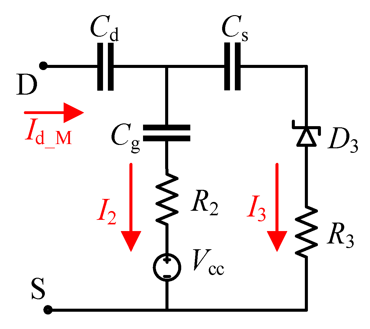
At t0, when the Vgs_M(max) occurs, M has been completely turned off, and the improved DVCC can be equivalent to the course shown in Figure 3 [29].
According to Figure 3, the first evaluation indicator can be expressed as
where Id_M is the drain current of M.
According to [29], at this time, Cg << Cs. The coefficient of the third term in Equation (15) is abbreviated as e + jf. Then, the real and imaginary parts of EI1 can be written as in Equations (17) and (18), respectively;
Since the parasitic capacitance of MOSFET is pF level (10−12), and the oscillation frequency of drain current is generally MHz level (106~108). Therefore, (Cg + Cs) >> (wCsCgR2 + wCsCgR3). Based on this, Equations (21) and (22) can be derived;
According to Equation (22), |EI1| is positively correlated with R3 and negatively correlated with R2. Therefore, the selection guide for these two resistors is to increase R2 and decrease R3 as much as possible. It is worth noting that this increase or decrease is not unlimited, which is described in more detail in the following subsection.
3.4.2. Measurement Error Constraint
During the on-oscillation state, with R3 decreasing, the measurement accuracy of the on-state voltage vds_on_osc gradually decreases. To make the relative error of the vds_on_osc measurement less than r%, R3 cannot be too small. This paper refers to this constraint relationship as the “measurement error constraint” (MEC).
During the on-oscillation state, vds_on_osc can be described as follows:
where vds_M is the drain–source voltage of M.
During this process, vds_on_osc gradually shifts from the on-oscillation state to the on-steady state in the form of a second-order oscillation. According to the structure of the improved DVCC, D3 is connected in reverse between A and B. Therefore, when vds_on_osc > 0, D3 is in the reverse cut-off state, and vout can be expressed as follows:
where RD3_off is the equivalent resistance of D3 when it is in the reverse cut-off state; Rds_M is the equivalent resistance of M.
Since M has been fully turned on at this stage, Rds_M has the same value as the on-state resistance of M. In addition, considering that D3 can be regarded as an open circuit at this time, the relationship between vout and vds_on_osc can be expressed as follows:
However, when vds_on_osc < 0, D3 is in the forward conduction state, and vout can be expressed as follows:
where RD3_on is the equivalent resistance of D3 when it is in the forward conduction state.
In this case, it is essential that the resistance of R3 not be too small, so that the measurement accuracy is not compromised due to the partial voltage of Rds_M. Therefore, restricted by MEC, R3 needs to meet the following condition:
Furthermore, Equation (27) is simplified to
where r% is generally around 5%.
3.4.3. Switching Speed Constraint
R2 is located at the gate of M. Therefore, when R2 increases, the gate charging and discharging speed of the gate driver are slowed down accordingly [29]. In an attempt to ensure that the switching speed of M is not slower than that of the DUT, R2 cannot be too large. This paper calls this constraint relationship the “switching speed constraint” (SSC).
In order to obtain the limit of R2, the influence of R2 on the rising speed of vgs_M is simplified as the influence of R2 on the charging time constant when M is turned on. According to Equations (5) and (10), when M is turned on, the amount of change in vgs_M is ((Vcc − vds_on) − (Vcc − VD3′)).
Therefore, restricted by SSC, R2 needs to meet the following condition:
where Vg_max is the gate−source voltage stability value of the DUT; Rg and Vth_DUT are the gate drive resistance and the threshold voltage of the DUT, respectively; and Cgs_M and Cgs_DUT are the gate−source parasitic capacitances of M and DUT, respectively.
Considering that VD3′ ≤ VD3, Equation (30) can be further simplified to
4. Simulation and Experimental Verification
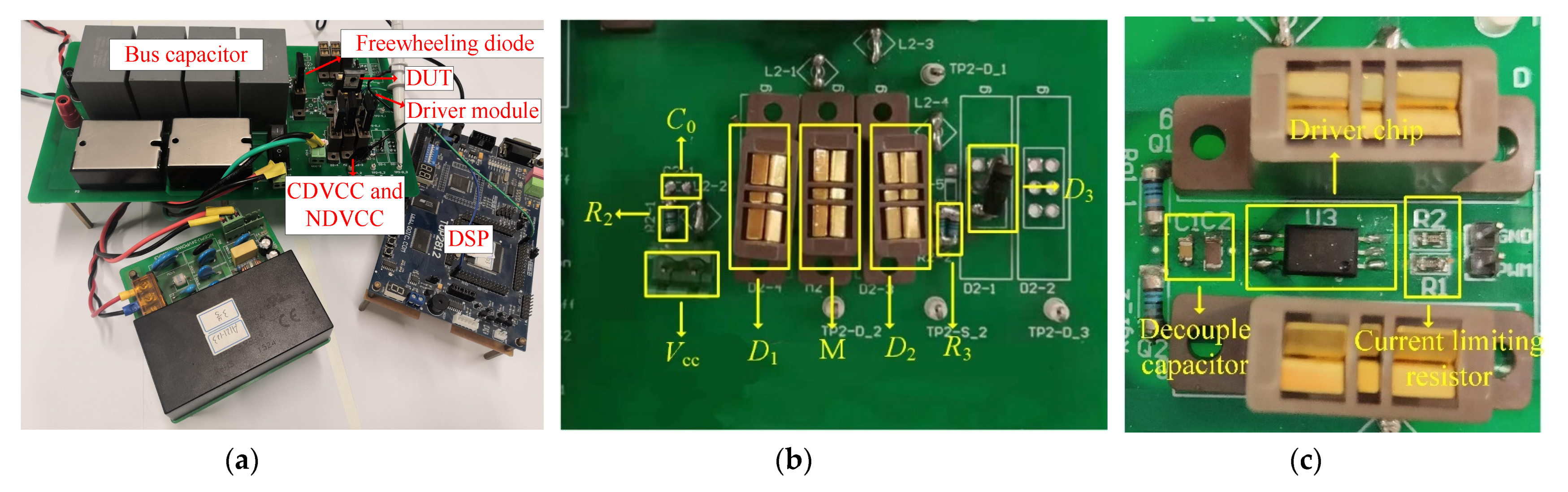
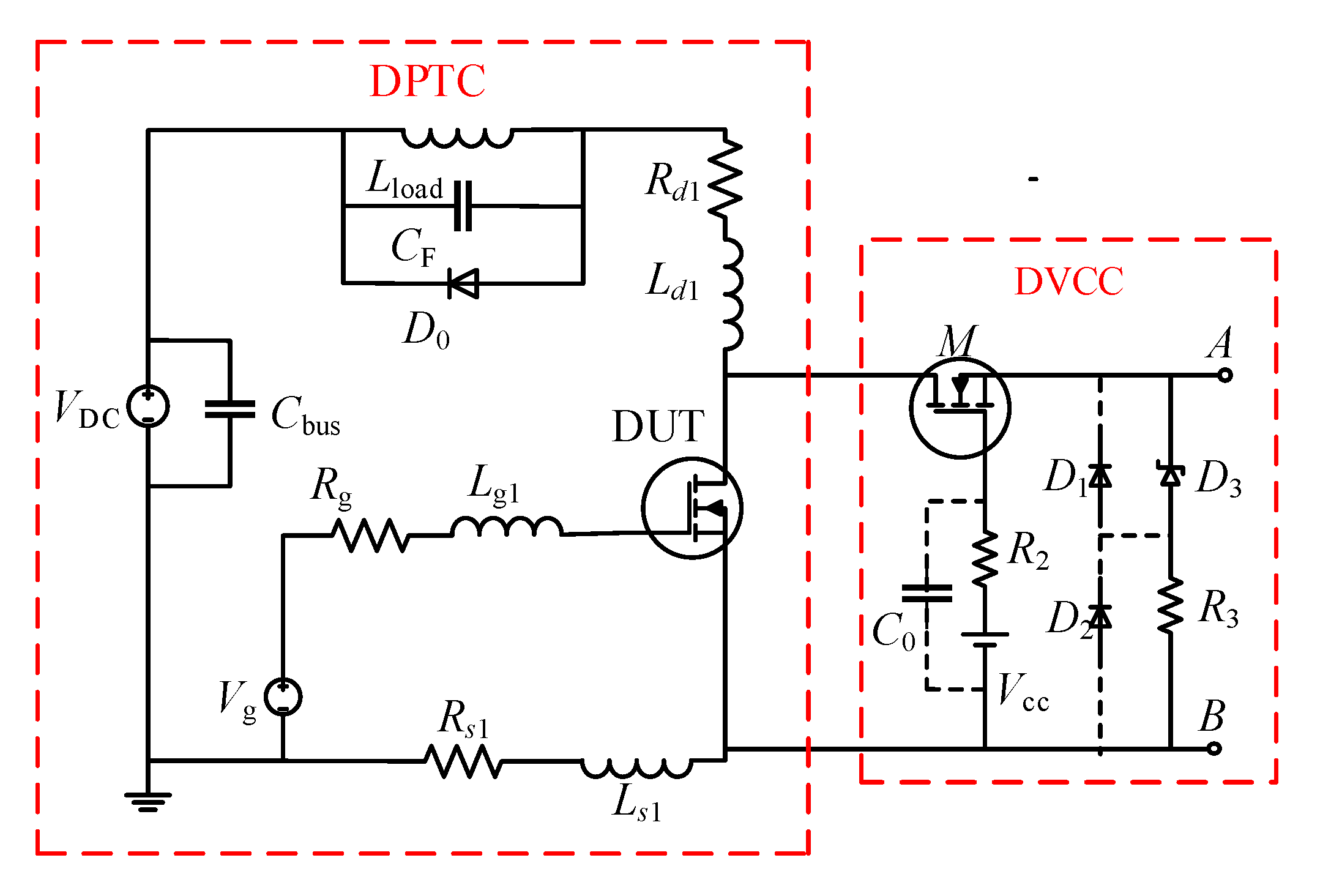
This paper set up a test platform integrating conventional DVCC and improved DVCC, as shown in Figure 4, to evaluate the measurement accuracy and work safety of the improved DVCC and the correctness of the selection theory. The primary circuit of the test platform is a double pulse test circuit (DPTC), including a DUT, freewheeling diode D0, bus capacitor Cbus, digital signal processing (DSP), and drive module Vg. DSP is used to transmit drive signals to control the turn-on and turn-off of the DUT.
The voltage clamp circuit comprises a MOSFET (M), DC source Vcc, gate resistance R2, source resistance R3, and Zener diode D3. In order to facilitate the comparison between the improved DVCC and conventional DVCC, the connectors for the gate-shunt capacitor C0 and the anti-parallel diodes D1 and D2 are reserved.
The specific experimental conditions are listed in Table 1. Both the DUT and the auxiliary device M are the 1200 V/31.6 A SiC MOSFET produced by CREE, while the freewheeling diode D0 is the SiC Schottky diode of the unified manufacturer.
According to the experimental platform shown in Figure 4, the corresponding equivalent simulation circuit is extracted, as shown in Figure 5. Inside the dotted frame on the right is the DVCC, while the double pulse circuit is in the dotted frame on the left, and its circuit components are shown in Table 2. The simulation models of DUT, M, and D0 are all from the semiconductor company that produces the device, and the parasitic parameters are extracted by finite element simulation software.
4.1. Conduction Loss Measurement Accuracy
4.1.1. Quantitative Simulation Analysis
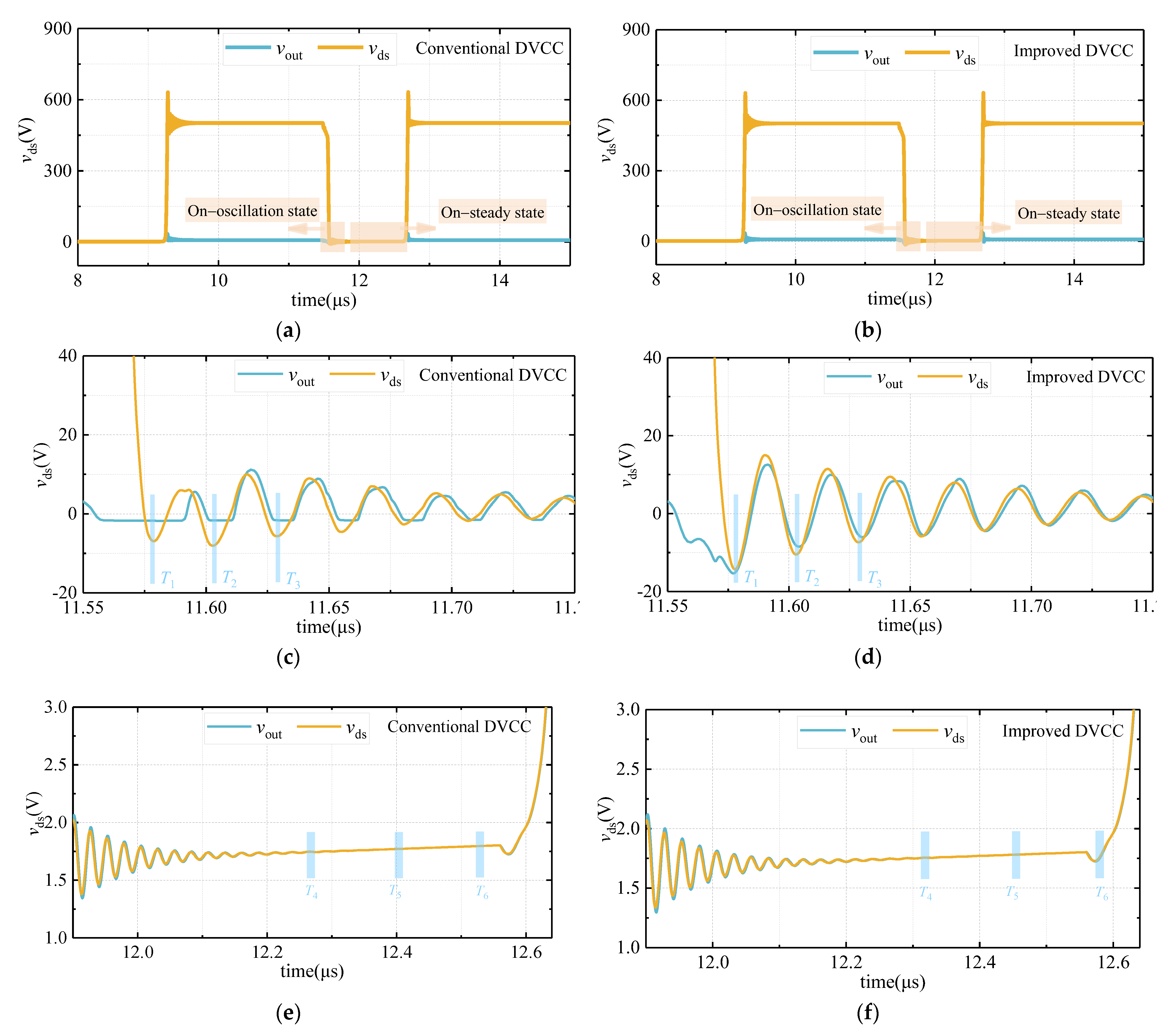
Since the oscilloscope cannot measure the accurate value of the on-state voltage vds_on, it is hard to quantitatively analyze the relative error between the output voltage vout and vds_on through experiments. Therefore, this work uses the simulation circuit shown in Figure 5 to compare the on-state voltage and conduction loss measurement accuracy between the conventional DVCC and the improved DVCC. Under the working condition that VDC is set to 500 V, the simulation results are shown in Figure 6.
In Figure 6, vds is the voltage waveform measured directly at the drain and source of the DUT. When the DUT is in the on state, vds = vds_on. As shown in Figure 6c, the conventional DVCC cannot measure a voltage less than −1.7 V, while the improved DVCC solves this problem (see Figure 6d). Table 3 selects three measurement points, which are located at the moments when the first, second, and third negative peaks of the drain–source voltage of the DUT occur, to compare the vds (actual value) and the output voltage vout. As shown in Table 3, during the on-oscillation state, the max voltage measurement relative error of the conventional DVCC can reach up to 78.8%, while the error value of the improved DVCC is reduced to less than 17.6%. The comparison results of vds (actual value) and vout during the on-steady state are shown in Table 4, which shows that the relative errors of the on-steady state voltage measured by the conventional DVCC and the improved DVCC are both within 1%. Furthermore, the conduction loss measurement errors of the conventional DVCC and the improved DVCC, as shown in Table 5, are 6.42% and 0.78%, respectively, which proves the high accuracy of the conduction loss measurement of the improved circuit.
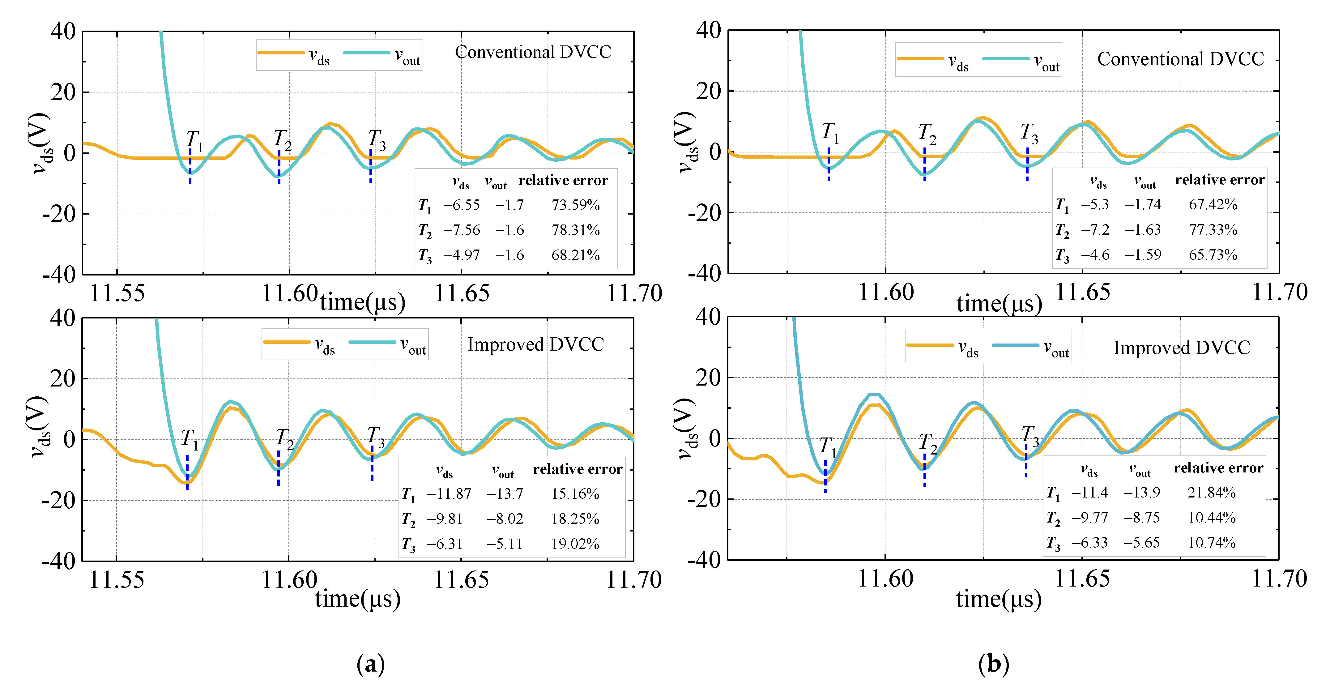
To more powerfully illustrate the reduction of conduction loss and on-state voltage measurement error, simulations under different voltages are supplemented. During the test, the VDC is set to 400 V and 600 V, respectively, and the measurement results are shown in Figure 7.
The relative error between vds (actual value) and vout during the on-oscillation state is shown in Figure 7. Compared with the conventional DVCC, the measurement relative error of the improved DVCC is significantly reduced. When VDC is 400 V and 600 V, the maximum relative errors are reduced from 78.31% and 77.33% to 19.02% and 21.84%, respectively. Furthermore, by comparing the conduction loss value measured by the conventional DVCC and the improved DVCC, it can be known that when the VDC is 400 V and 600 V, the relative errors are reduced from 6.60% and 6.85% to 1.07% and 1.65%, respectively, which is shown in Table 6.
4.1.2. Qualitative Experimental Verification
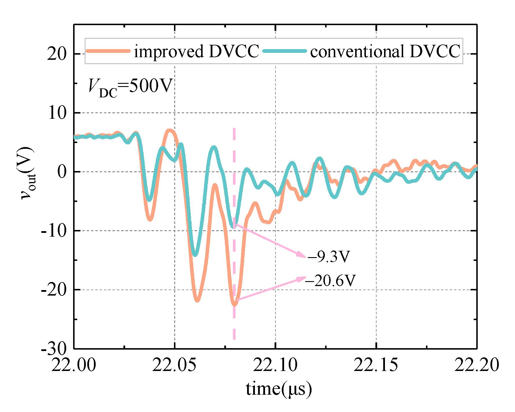
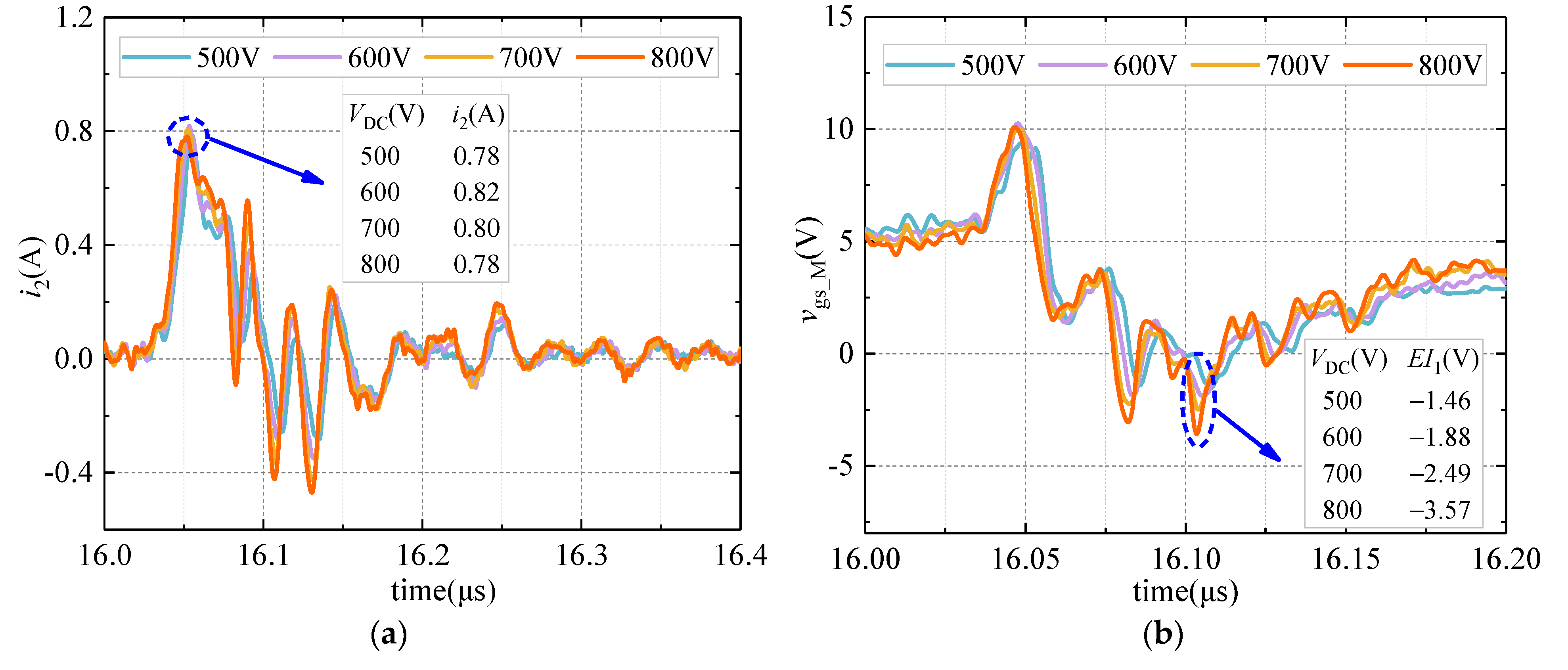
The comparative experiment of the on-oscillation state voltage measurement is carried out in this section. Under the same working condition, the conventional DVCC and improved DVCC are used to measure the on-state voltage of the DUT, respectively. The voltage negative overshoot measured by the two circuits is compared, and the result is shown in Figure 8.
It can be seen from Figure 8 that compared to the improved DVCC, the drain–source voltage negative overshoot measured by the conventional DVCC is significantly reduced. Under the test voltage conditions of 500 V, the measurement result of the voltage negative overshoot is reduced by 11.3 V, which is consistent with the theoretical analysis in Section 2.2.1 and the simulation verification in Section 4.2.1.
4.2. Working Security of Auxiliary Device MOSFET
4.2.1. Comparison of Work Security of M in Conventional DVCC and Improved DVCC
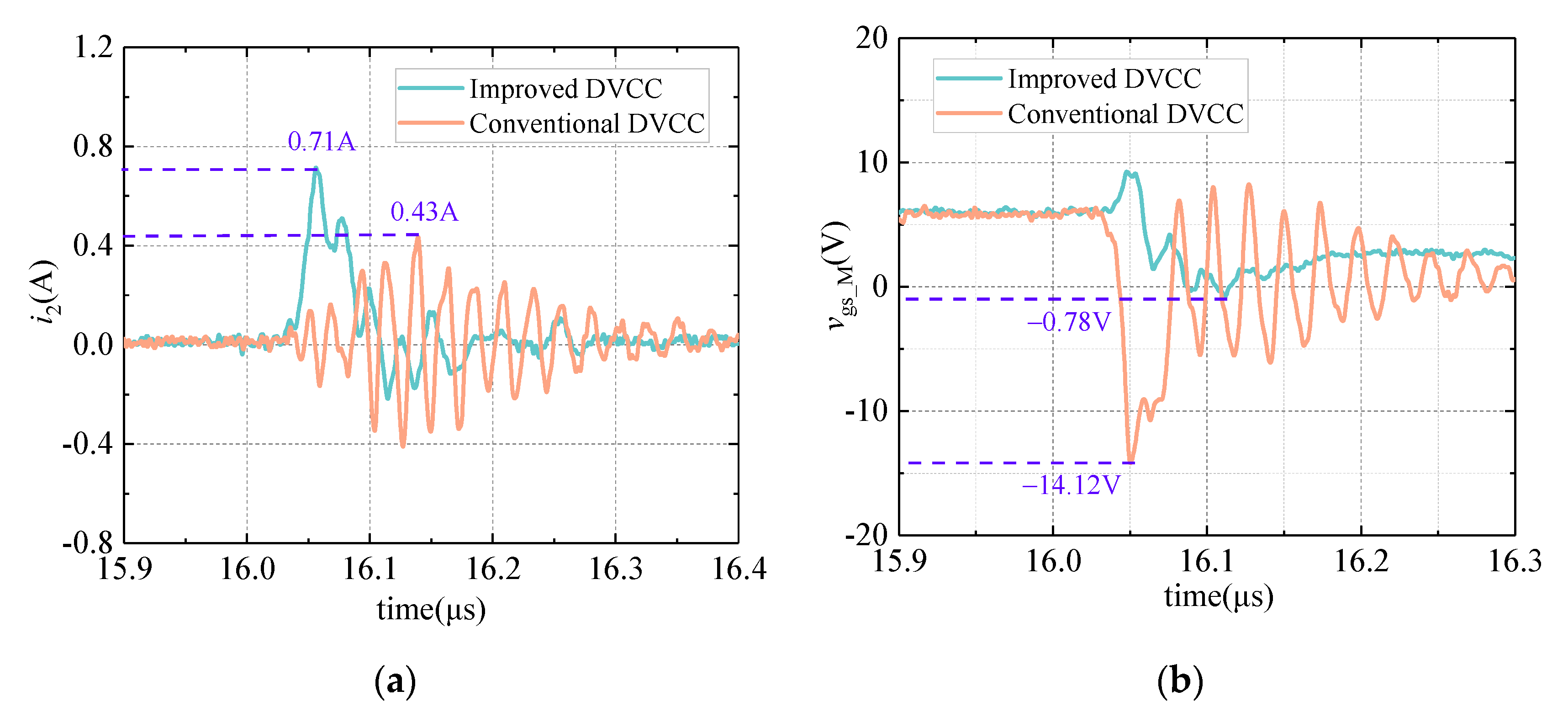
The experiments are carried out utilizing the test platform shown in Figure 4, with the primary circuit (DPTC) operating conditions unchanged. Due to the presence of the gate-shunt capacitance, the gate–source voltage negative overshoot of M may exceed its tolerance limit. Therefore, the VDC is set to 400 V to ensure the safety of M. The current waveform flowing through Vcc and the gate−source voltage waveform of M are shown in Figure 9.
The improved DVCC reduces the absolute value of Vgs_M(max) from 14.12 to 0.78 V but increases the max current flowing through Vcc from 0.43 to 0.71 A. As seen, the increase in current can be ignored because it is still far less than the impulse tolerance of the DC voltage supply. However, according to the datasheet, the gate−source withstand voltage limit Vgs_limit of M is only −10 V. Therefore, the reduction of Vgs_M(max) from −14.12 to −0.78 V makes M out of unsafe conditions, which significantly improves the work security of M.
4.2.2. Work Security of M and Vcc at Higher Voltages
To study the working safety of Vcc and M in the improved DVCC under higher voltages (500 V, 600 V, 700 V, 800 V), related experiments are carried out. The circuit components are selected based on the selection theory proposed in this article to ensure the safety of the experiments. Since the target maximum experimental voltage is 800 V, VD3 is set to 7.5 V, Vcc is set to 7 V, R2 is selected to 50 Ω, and R3 is selected to 5 Ω for the experiment. The results are shown in Figure 10.
As shown in Figure 10, at higher voltages, the gate–source voltage negative overshoot of M (EI1) is always within the maximum rating of the gate–source voltage of M. In addition, at the moment of turning off, the maximum current flowing through the DC source (Vcc) is about 0.8 A, which is much smaller than the impulse current tolerance of the DC source. Therefore, the improved circuit proposed in this article can still work effectively and safely under high-voltage conditions.
4.3. Selection Method of Vcc and VD3
According to the working principle of the double pulse circuit and the device parameters of the DUT, when the off-state voltage of the DUT is 800 V, the maximum on-state voltage Von_max can reach 3.2 V. Based on the selection mechanism and detailed analyses in Section 3, set Vcc to 7 V and VD3 to 7.5 V for the experiment. The results are depicted in Figure 11.
As shown in Figure 11, under different voltages, when the DUT is in the on state, it always meets EI2 > Vth_M, ensuring that M is normally turned on. When the DUT is in the off state, it satisfies EI3 < Vth_M, so that M is also in the off state. The experimental results prove the rationality of the selection method of Vcc and VD3.
4.4. Selection Method of R2 and R3
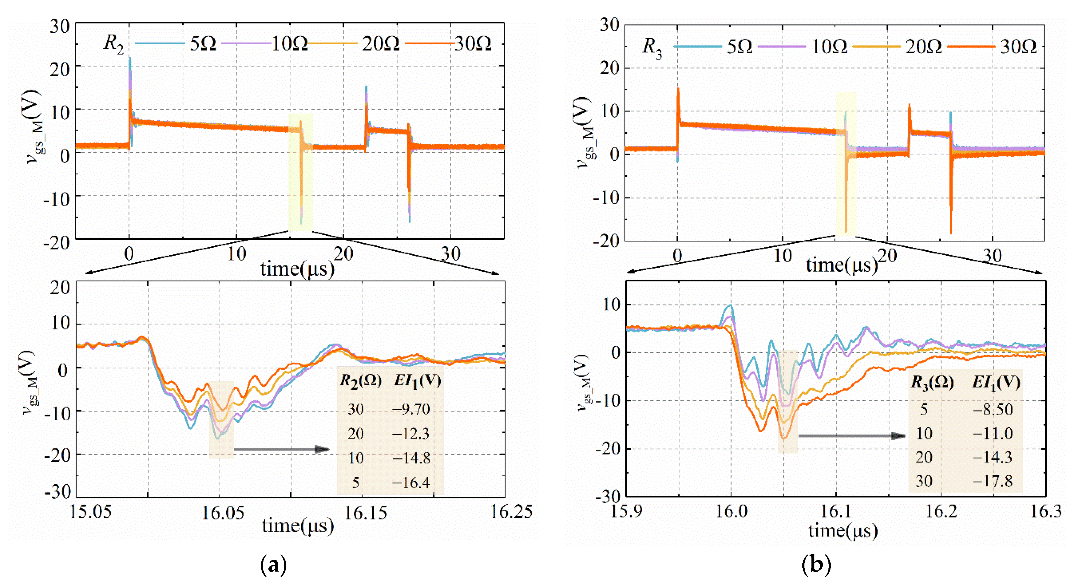
According to Equations (28) and (31), R3 > 1.52 Ω and R2 < 55 Ω while meeting SSC and MEC. Using the controlled variable method, when Vcc, VD3, and R3 are determined, set R2 to 5 Ω, 10 Ω, 20 Ω, and 30 Ω for the experiments. Figure 12a demonstrates the measured EI1 in the case of different R2. Moreover, when R2 is determined, set the resistance of R3 to 5 Ω, 10 Ω, 20 Ω, and 30 Ω for the experiments. The variation of EI1 with R3 is shown in Figure 12b.
As described in Figure 12, EI1 decreases with the increase in R2, and it increases with the increase in R3. The experimental results effectively verify the correctness of the theoretical analysis indicated in Section 3. When choosing R2, the resistance should be as large as possible while meeting SSC. In contrast, when choosing R3, the resistance should be as small as possible while completing MEC.
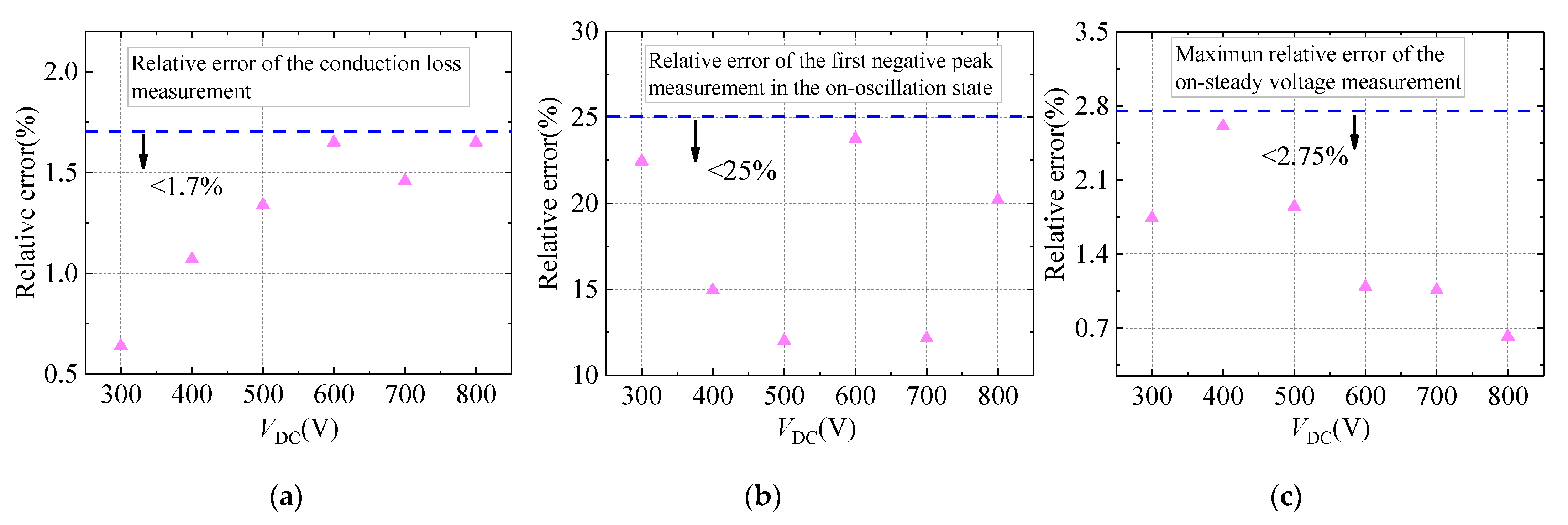
4.5. Error Analysis
The size of the error in on-state voltage and conduction loss measurement, using the improved DVCC, is further analyzed to highlight the accuracy over different working conditions. Based on the circuit shown in Figure 5, the on-state voltage of the DUT is measured by the improved DVCC under the VDC of 300 V, 400 V, 500 V, 600 V, 700 V, and 800 V. Subsequently, utilizing the measured on-state voltage, the conduction loss is calculated. Furthermore, the measurement results of improved DVCC are compared with the actual value to get the relative error, which is shown in Figure 13.
It can be seen from Figure 13 that when using the improved DVCC to measure the conduction loss of the DUT, the relative error between the measurement result and the actual value remains below 1.7%. In addition, at the moment of turning on, the measurement relative error of the first negative peak is kept within 25%. Moreover, in the on-steady state, the maximum relative error of the on-steady state voltage measurement is within 2.75%. The above data effectively prove the high measurement accuracy of the improved DVCC.
5. Conclusions
An improved DVCC topology for measuring the conduction loss of power semiconductor devices is proposed and fully characterized in this article. The proposed DVCC, in comparison with the existing designs (conventional DVCC) through simulation and experimentation, shows better accuracy and higher security. During the on-oscillation state, the maximum relative error of the on-state voltage measurement decreased from 78.8% to 17.6%, and the on-state voltage measurement accuracy is greatly improved. Furthermore, the relative error of the total conduction loss measurement of the two on-state stages is reduced from 6.42% to 0.78%, which is one of the critical contributions of the proposed approach. Another key advantage of the improved DVCC is that it improves the working security of M, which is embodied in the reduction of the gate−source voltage negative overshoot of the auxiliary device MOSFET from −14.12 to 0.78 V. In addition, the influence of component parameters on the circuit performance of the improved DVCC is discussed, and three electrical quantities are extracted as the judgment indicators for the component selection, including the gate−source voltage negative overshoot (Vgs_M(max)) of M, the gate−source voltage vgs_M(on) of M when the DUT is in the on state, and the gate−source voltage vgs_M(off) of M when the DUT is in the off state. Finally, the component selection criteria are given and validated by experimental results. First, the switching speed and blocking voltage level of M should be consistent with or better than the DUT. Second, in the case of meeting VCEW, the breakdown voltage of the Zener diode (D3) should be selected to be a small value. Third, under the conditions of fulfilling MEC and SSC, the selection guide for these two resistors is to increase R2 and decrease R3 as much as possible.
Author Contributions
Conceptualization, Q.Y., Z.Z., P.S., and B.Z.; methodology, Q.Y.; software, Q.Y. and Z.Z.; validation, Q.Y., P.S., and Z.Z.; formal analysis, Q.Y. and Y.C.; investigation, Q.Y.; resources, Q.Y.; data curation, B.Z.; writing—original draft preparation, Q.Y. and P.S.; writing—review and editing, Q.Y.; visualization, Z.Z.; supervision, B.Z.; project administration, Q.Y., and P.S.; funding acquisition, Z.Z. All authors have read and agreed to the published version of the manuscript.
Funding
This work was supported by State Grid science and technology projects (Electrical characterization and screening method of press-pack IGBT chip (grant no. 5455GB190007).
Institutional Review Board Statement
Not applicable.
Informed Consent Statement
Not applicable.
Data Availability Statement
The data used for the manuscript are available for researchers on request.
Conflicts of Interest
The authors declare no conflict of interest.
References
- Zhao, Z.M.; Shi, B.C.; Zhu, Y.C. Control Technologies for Power Electronic Hybrid Systems in High-voltage High-power Applications: A Review. High Volt. Eng. 2019, 45, 2017–2027. [Google Scholar]
- Lagier, T.; Ladoux, P.; Dworakowski, P. Potential of silicon carbide MOSFETs in the DC/DC converters for future HVDC offshore wind farms. High Volt. 2017, 2, 233–243. [Google Scholar] [CrossRef]
- Gareau, J.; Hou, R.; Emadi, A. Review of Loss Distribution, Analysis, and Measurement Techniques for GaN HEMTs. IEEE Trans. Power Electron. 2020, 35, 7405–7418. [Google Scholar] [CrossRef]
- Fuentes, C.D.; Müller, M.; Bernet, S.; Kouro, S. SiC-MOSFET or Si-IGBT: Comparison of Design and Key Characteristics of a 690 V Grid-Tied Industrial Two-Level Voltage Source Converter. Energies 2021, 14, 3054. [Google Scholar] [CrossRef]
- Cai, Y.M.; Zhao, Z.B.; Liang, S.; Sun, P.; Yang, F. Influence of Parasitic Parameters of Commutation Path on Switching Characteristics of Silicon Carbide MOSFET. High Volt. Eng. 2021, 47, 603–614. [Google Scholar]
- Sun, P.; Zhao, Z.; Cai, Y.; Ke, J.; Cui, X.; Ji, B. Analytical model for predicting the junction temperature of chips considering the internal electrothermal coupling inside SiC metal-oxide-semiconductor field-effect transistor modules. IET Power Electron. 2020, 13, 436–444. [Google Scholar]
- Chen, M.; Hu, A.; Tang, Y.; Wang, B. Modeling Analysis of IGBT Thermal Model High Voltage Engineering. High Volt. Eng. 2011, 37, 453–459. [Google Scholar]
- Lei, W.J.; Liu, J.J.; Lv, G.T.; Lv, C.L.; Cao, R. Review of Reliability Comprehensive Analysis and Evaluation Methods for Key Components and System of Large Capacity Power Electronic Equipment. High Volt. Eng. 2020, 46, 3353–3361. [Google Scholar]
- Ladoux, P.; Blaquiere, J.M.; Alvarez, S.; Carroll, E.; Streit, P. Test bench for the characterisation of experimental low voltage IGCTs. In Proceedings of the 35th Annual IEEE Power Electronics Specialists Conference (PESC 04), Aachen, Germany, 20–25 June 2004. [Google Scholar]
- Anurag, A.; Acharya, S.; Bhattacharya, S. An Accurate Calorimetric Loss Measurement Method for SiC MOSFETs. IEEE J. Emerg. Sel. Top. Power Electron. 2020, 8, 1644–1656. [Google Scholar] [CrossRef]
- Li, H.; Li, X.; Zhang, Z.; Wang, J.; Liu, L.; Bala, S. A Simple Calorimetric Technique for High-Efficiency GaN Inverter Transistor Loss Measurement. In Proceedings of the 5th IEEE Workshop on Wide Bandgap Power Devices and Applications (WiPDA), Albuquerque, NM, USA, 30 October–1 November 2017. [Google Scholar]
- Johannesson, D.; Nawaz, M. Assessment of PSpice Model for Commercial SiC MOSFET Power Modules. In Proceedings of the 3rd IEEE Workshop on Wide Bandgap Power Devices and Applications (WiPDA), Blacksburg, VA, USA, 2–4 November 2015. [Google Scholar]
- Hsin-Ju, C.; Kusic, G.L.; Reed, G.F. Comparative PSCAD and Matlab/Simulink simulation models of power losses for SiC MOSFET and Si IGBT devices. In Proceedings of the 2012 IEEE Power and Energy Conference at Illinois, Champaign, IL, USA, 24–25 February 2012. [Google Scholar]
- Prasad, J.S.S.; Prasad, K.N.V.; Narayanan, G. Device Loss and Thermal Characteristics of High Power PWM Converters. In Proceedings of the 8th IEEE India International Conference on Power Electronics (IICPE), Jaipur, India, 13–15 December 2018. [Google Scholar]
- Lim, H.; Hwang, J.; Kwon, S.; Baek, H.; Uhm, J.; Lee, G. A Study on Real Time IGBT Junction Temperature Estimation Using the NTC and Calculation of Power Losses in the Automotive Inverter System. Sensors 2021, 21, 2454. [Google Scholar] [CrossRef]
- Ahmed, M.H.; Wang, M.; Hassan, M.A.S.; Ullah, I. Power Loss Model and Efficiency Analysis of Three-Phase Inverter Based on SiC MOSFETs for PV Applications. IEEE Access 2019, 7, 75768–75781. [Google Scholar] [CrossRef]
- Zhang, L.; Yuan, X.; Wu, X.; Shi, C.; Zhang, J.; Zhang, Y. Performance Evaluation of High-Power SiC MOSFET Modules in Comparison to Si IGBT Modules. IEEE Trans. Power Electron. 2019, 34, 1181–1196. [Google Scholar] [CrossRef]
- Gelagaev, R.; Jacqmaer, P.; Driesen, J. A Fast Voltage Clamp Circuit for the Accurate Measurement of the Dynamic ON-Resistance of Power Transistors. IEEE Trans. Ind. Electron. 2015, 62, 1241–1250. [Google Scholar] [CrossRef]
- Carsten, B. Clipping preamplifier provides accurate measurement of transistor conduction voltages. In Proceedings of the 31st International Power Conversion Electronic Conference Exhibition, Long Beach, CA, USA, 9–15 September 1996. [Google Scholar]
- Pokryvailo, A.; Carp, C. Accurate Measurement of on-State Losses of Power Semiconductors. In Proceedings of the Proceedings of the 2008 IEEE International Power Modulators and High Voltage Conference, Las Vegas, NV, USA, 27–31 May 2008. [Google Scholar]
- Ren, L.; Shen, Q.; Gong, C. A Voltage Clamp Circuit for the Real-Time Measurement of the On-State Voltage of Power Transistors. In Proceedings of the 8th Annual IEEE Energy Conversion Congress and Exposition (ECCE), Milwaukee, WI, USA, 18–22 September 2016. [Google Scholar]
- Ghimire, P.; de Vega, A.R.; Beczkowski, S.; Munk-Nielsen, S.; Rannested, B.; Thogersen, P.B. An online V-ce measurement and temperature estimation method for high power IGBT module in normal PWM operation. In Proceedings of the International Power Electronics Conference (IPEC-ECCE-ASIA), Hiroshima, Japan, 18–21 May 2014. [Google Scholar]
- Bęczkowski, S.; Ghimre, P.; de Vega, A.R.; Munk-Nielsen, S.; Rannestad, B.; Thøgersen, P. Online Vce measurement method for wear-out monitoring of high power IGBT modules. In Proceedings of the 2013 15th European Conference on Power Electronics and Applications (EPE), Lille, France, 2–6 September 2013. [Google Scholar]
- Yu, B.; Wang, L.; Ahmed, D. Drain-Source Voltage Clamp Circuit for Online Accurate ON-State Resistance Measurement of SiC MOSFETs in DC Solid-State Power Controller. IEEE J. Emerg. Sel. Top. Power Electron. 2020, 8, 331–342. [Google Scholar] [CrossRef]
- Guacci, M.; Bortis, D.; Kolar, J.W. On-state voltage measurement of fast switching power semiconductors. CPSS Trans. Power Electron. Appl. 2018, 3, 163–176. [Google Scholar] [CrossRef]
- Li, R.; Wu, X.; Yang, S.; Sheng, K. Dynamic on-State Resistance Test and Evaluation of GaN Power Devices Under Hard- and Soft-Switching Conditions by Double and Multiple Pulses. IEEE Trans. Power Electron. 2019, 34, 1044–1053. [Google Scholar] [CrossRef]
- Lu, B.; Palacios, T.; Risbud, D.; Bahl, S.; Anderson, D.I. Extraction of Dynamic On-Resistance in GaN Transistors: Under Soft- and Hard-Switching Conditions. In Proceedings of the 2011 IEEE Compound Semiconductor Integrated Circuit Symposium (CSICS), Waikoloa, HI, USA, 16–19 October 2011. [Google Scholar]
- Wang, J.; Chung, H.S.-H.; Li, R.T.-H. Characterization and Experimental Assessment of the Effects of Parasitic Elements on the MOSFET Switching Performance. IEEE Trans. Power Electron. 2013, 28, 573–590. [Google Scholar] [CrossRef]
- Ke, J.J.; Zhao, Z.B.; XIe, Z.K.; Xu, P.; Cui, X. Analytical Switching Transient Model for Silicon Carbide MOSFET under the Influence of Parasitic Parameters. Trans. China Electrotech. Soc. 2018, 33, 1762–1774. [Google Scholar]
- Gelagaev, R.; Jacqmaer, P.; Everts, J.; Driesen, J. A Novel Voltage Clamp Circuit for the Measurement of Transistor Dynamic On-Resistance. In Proceedings of the 29th Annual IEEE International Instrumentation and Measurement Technology Conference (I2MTC), Graz, Austria, 13–16 May 2012. [Google Scholar]
Figure 1.
The schematic diagram of the conventional DVCC.

Figure 2.
The schematic diagram of the improved DVCC.

Figure 3.
Equivalent circuit of the improved DVCC.

Figure 4.
Test platform. (a) Test platform overview; (b) DVCC section; (c) gate driver.

Figure 5.
Equivalent simulation circuit.

Figure 6.
vout and vds waveform comparison. (a) Waveform overview of the conventional DVCC; (b) waveform overview of the improved DVCC; (c) waveform of the conventional DVCC during the on-oscillation state; (d) waveform of the improved DVCC during the on-oscillation state; (e) waveform of the conventional DVCC during the on-steady state; (f) waveform of the improved DVCC during the on-steady state.

Figure 7.
vds and vout waveform comparison during the on-oscillation state. (a) VDC = 400 V; (b) VDC = 600 V.
Figure 7.
vds and vout waveform comparison during the on-oscillation state. (a) VDC = 400 V; (b) VDC = 600 V.

Figure 8.
vout waveform comparison during the on-oscillation state.

Figure 9.
The current waveform flowing through Vcc and the gate−source voltage waveform of M. (a) Current waveform; (b) voltage waveform.
Figure 9.
The current waveform flowing through Vcc and the gate−source voltage waveform of M. (a) Current waveform; (b) voltage waveform.

Figure 10.
The current waveform flowing through Vcc and the gate−source voltage waveform of M under higher voltages. (a) Current waveform; (b) voltage waveform.
Figure 10.
The current waveform flowing through Vcc and the gate−source voltage waveform of M under higher voltages. (a) Current waveform; (b) voltage waveform.

Figure 11.
The gate-source voltage waveform of M under different voltages (Vcc = 7 V, VD3 = 7.5 V).

Figure 12.
The variation of EI1 with R2 and R3. (a) With R2; (b) with R3.

Figure 13.
The measurement relative error of improved DVCC. (a) Conduction loss; (b) on-oscillation state voltage; (c) on-steady state voltage.
Figure 13.
The measurement relative error of improved DVCC. (a) Conduction loss; (b) on-oscillation state voltage; (c) on-steady state voltage.


Table 1.
Test conditions.
| Parameters | Value |
|---|---|
| VDC | 400 V/500 V |
| Cbus | 200 μF |
| Lload | 0.7 mH |
| Vg | +20 V/−5 V |
Table 2.
Circuit parameter index.
| Symbol | Parameters |
|---|---|
| Lg1 | Parasitic inductance of the gate of the DUT |
| Ld1 | Parasitic inductance of the drain of the DUT |
| Ls1 | Parasitic inductance of the source of the DUT |
| Rd1 | Parasitic resistance of the drain of the DUT |
| Rs1 | Parasitic resistance of the source of the DUT |
| Rg | Gate drive resistance of the DUT |
| D0 | Freewheeling diode |
| VDC | Bus voltage |
Table 3.
Comparison of vds and vout during the on-oscillation state.
| Time | Circuit | vds/V | vout/V | Relative Error |
|---|---|---|---|---|
| T1 | Conventional | −6.9 | −1.7 | 75.4% |
| Improved | −14.3 | −15.3 | 7.0% | |
| T2 | Conventional | −8.0 | −1.7 | 78.8% |
| Improved | −10.3 | −8.5 | 17.5% | |
| T3 | Conventional | −5.6 | −1.7 | 77.0% |
| Improved | −7.4 | −6.1 | 17.6% |
Table 4.
Comparison of vds and vout during the on-steady state.
| Time | Circuit | vds/V | vout/V | Relative Error |
|---|---|---|---|---|
| T4 | Conventional | 1.710399 | 1.717680 | 0.43% |
| Improved | 1.715286 | 1.724388 | 0.53% | |
| T5 | Conventional | 1.753108 | 1.752805 | 0.02% |
| Improved | 1.752987 | 1.752228 | 0.04% | |
| T6 | Conventional | 1.800825 | 1.800813 | 0.0007% |
| Improved | 1.800945 | 1.800930 | 0.0009% |
Table 5.
Comparison of conduction loss measurement.
| Circuit | Measure Directly/μJ | Measure by DVCC/μJ | Relative Error |
|---|---|---|---|
| Conventional | 35.733 | 38.027 | 6.42% |
| Improved | 37.010 | 36.721 | 0.78% |
Table 6.
Comparison of conduction loss measurement under different voltages.
| Voltage | Circuit | Measure Directly/μJ | Measure by DVCC/μJ | Relative Error |
|---|---|---|---|---|
| 400 V | Conventional | 22.40 | 23.87 | 6.60% |
| Improved | 23.32 | 23.07 | 1.07% | |
| 600 V | Conventional | 52.92 | 56.55 | 6.85% |
| Improved | 54.52 | 53.62 | 1.65% |
Publisher’s Note: MDPI stays neutral with regard to jurisdictional claims in published maps and institutional affiliations. |
© 2021 by the authors. Licensee MDPI, Basel, Switzerland. This article is an open access article distributed under the terms and conditions of the Creative Commons Attribution (CC BY) license (https://creativecommons.org/licenses/by/4.0/).
Share and Cite
MDPI and ACS Style
Yu, Q.; Zhao, Z.; Sun, P.; Zhao, B.; Cai, Y. An Improved Voltage Clamp Circuit Suitable for Accurate Measurement of the Conduction Loss of Power Electronic Devices. Sensors 2021, 21, 4285. https://doi.org/10.3390/s21134285
AMA Style
Yu Q, Zhao Z, Sun P, Zhao B, Cai Y. An Improved Voltage Clamp Circuit Suitable for Accurate Measurement of the Conduction Loss of Power Electronic Devices. Sensors. 2021; 21(13):4285. https://doi.org/10.3390/s21134285
Chicago/Turabian StyleYu, Qiuping, Zhibin Zhao, Peng Sun, Bin Zhao, and Yumeng Cai. 2021. "An Improved Voltage Clamp Circuit Suitable for Accurate Measurement of the Conduction Loss of Power Electronic Devices" Sensors 21, no. 13: 4285. https://doi.org/10.3390/s21134285
Note that from the first issue of 2016, this journal uses article numbers instead of page numbers. See further details here.