Proceeding Paper

Fabrication of Diamond Membranes by Femtosecond Laser Ablation for MEMS Sensor Applications †

1
Research Center for Microtechnology, Vorarlberg University of Applied Sciences, 6850 Dornbirn, Austria
2
Institute of Physics, Czech Academy of Sciences, 162 00 Prague 6, Czech Republic
3
Institute of Electrical Engineering, Slovak Academy of Sciences, 841 04 Bratislava, Slovakia
*
Author to whom correspondence should be addressed.
Presented at the 4th International Conference nanoFIS 2020—Functional Integrated nano Systems, Graz, Austria, 2–4 November 2020.
Proceedings 2020, 56(1), 13; https://doi.org/10.3390/proceedings2020056013
Published: 10 December 2020

Abstract

:
We present the feasibility in fabricating membranes and cantilevers made of diamond grown on Si/SiO2 substrates by femtosecond laser ablation. In the ablation process, we generated nano- and microstructures on the membrane surface. Such laser-induced periodic surface structures (LIPSS) are useful in tailoring the surface chemistry. In combination with wet or reactive ion etching, smooth membranes were generated.

1. Introduction

Diamond and other wide-bandgap materials can be effectively used in specialized sensor applications. However, their micromachining is somewhat challenging due to their chemical resistivity and mechanical hardness. Femtosecond laser ablation provides a precise fabrication of diamond without overheating of the ablated material as visible and near-infrared light is generally not absorbed. Recently, we demonstrated a laser ablation method providing SiC membranes and laser-induced periodic surface structures (LIPSS) in the micro- and nanometer range for MEMS and sensor applications [1,2,3]. We observed the formation of high-spatial frequency LIPSS (HSFL) on the backside of metal-coated SiC membranes [2,3]. This enhances the functionalization of diamond membranes or cantilevers for specific chemical sensor applications, e.g., gas sensors, solar cells photocatalysis, electronic devices and batteries. In this work, fabrication of diamond membranes by the laser ablation technique with regard to the issues and solutions is presented.

2. Materials and Methods
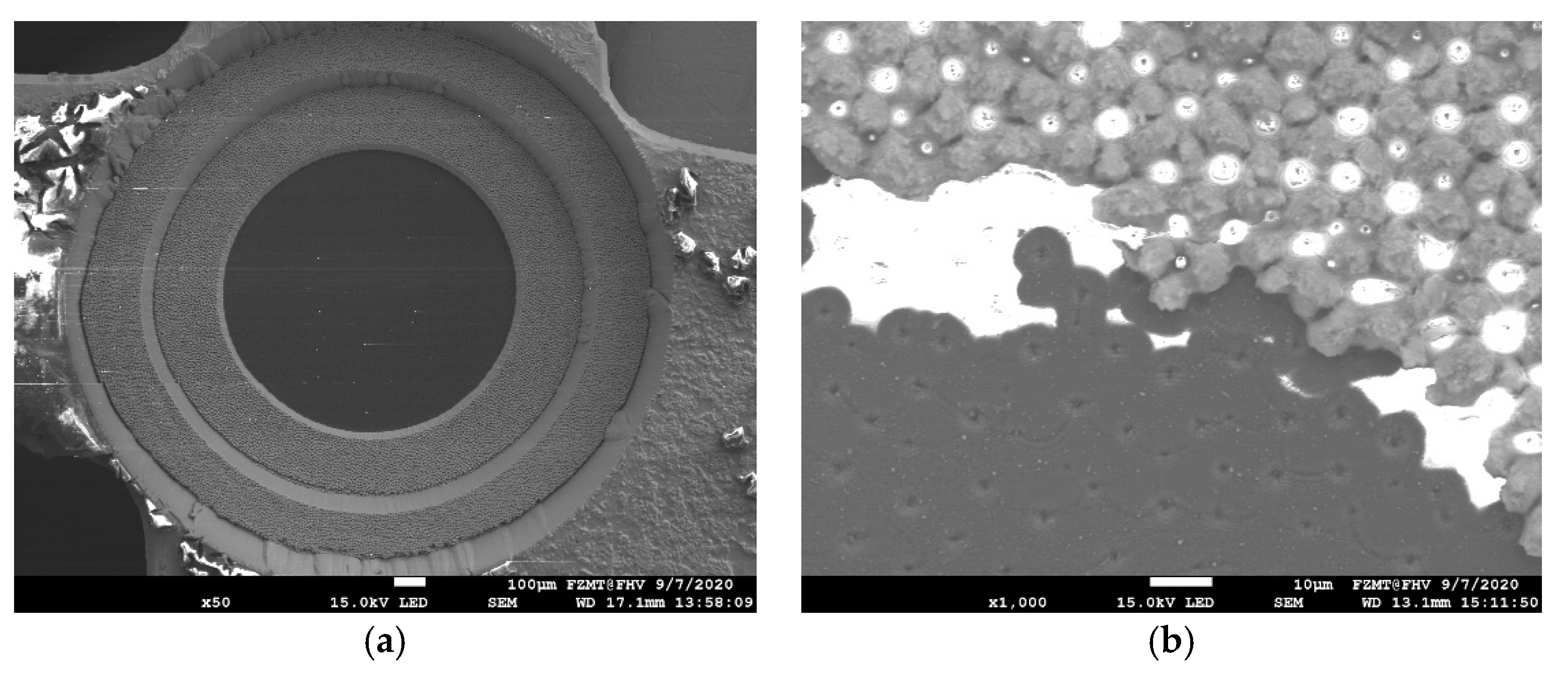
The diamond films were deposited on 525 µm thick (100) Si substrates (covered by 1.3 µm thick SiO2 layer) with an ellipsoidal cavity microwave plasma reactor. Before diamond chemical vapor deposition (CVD), the substrates were ultrasonically seeded by nanodiamond powder in DI water. The deposition conditions were as follows: MW power 4.2 kW, pressure 90 mbar, gas mixture 5% CH4 and 1.5% CO2 to H2, deposition temperature 960 °C, deposition time 16 and 32 hours, respectively, corresponding to diamond film thicknesses of approximately 7.2 and 21.7 µm. For laser ablation, a femtosecond (fs) laser (SPIRIT from Spectra Physics) was applied. For the experiments, we used the 1 MHz and 520 nm setting but picked only every tenth pulse to obtain an ablation pulse frequency of 100 kHz. The line distance between consecutive scans was 5 µm and the respective focus diameter of the 170 mm scanner lens was approximately 18 µm. The scan speed was set to 500 mm/s.

3. Results

The formation of pinholes on the membrane and elongated cavities at the corners of the bore in Si can be significantly reduced by rotating the direction of the laser polarization during the ablation procedure [3]. Due to the sufficient higher ablation threshold of diamond with respect to Si, we reduced the bore diameter in three steps from 2 to 1.5 to 1 mm (to attenuate the effect of the cavity formation at the corner, see Figure 1). An entire production of a membrane by selective laser ablation was possible after the removal of about 525 µm Si which required at least 700 consecutive ablation scans. This gave time to generate laser-induced surface structures and pinholes. Si masking effects had only a minor impact on the surface quality of the predominately selectively ablated diamond (Figure 1b). In the lower diagonal section of Figure 1b, the SiO2/Si layers on top of the diamond membrane were removed. The pinholes in the Si structure caused no excessive ablation at the diamond surface, and only shallow notches about 1 µm in diameter were generated. It is feasible to selectively remove the remaining SiO2 layer in the ablation process without destroying the 22 µm thick diamond membrane. In an earlier work, we produced 14 µm thick glass membranes [4], but the material properties of the deposited diamond layer on Si/SiO2 are promising to generate even thinner membranes in future attempts by laser ablation only.

Author Contributions

Conceptualization, A.K. and G.V.; methodology, J.Z., S.K. and T.I.; formal analysis, J.Z. and L.G.; investigation, T.I., J.Z., G.V.; writing—original draft preparation, J.Z.; writing—review and editing, G.V., T.I.; visualization, L.G.; supervision, A.K. All authors have read and agreed to the published version of the manuscript.

Funding

This research was funded by the Programme for Funding Multilateral Scientific and Technological Cooperation Projects in the Danube Region, grant No. DS-FR-19-0051 (grant No. 8X20035).

Conflicts of Interest

The authors declare no conflict of interest.

References

  1. Vanko, G.; Hudek, P.; Zehetner, J.; Dzuba, J.; Choleva, P.; Kutiš, V.; Vallo, M.; Rýger, I.; Lalinský, T. Bulk micromachining of SiC substrate for MEMS sensor applications. Microelectron. Eng. 2013, 110, 260–264. [Google Scholar] [CrossRef]
  2. Zehetner, J.; Kraus, S.; Lucki, M.; Vanko, G.; Dzuba, J.; Lalinsky, T. Manufacturing of membranes by laser ablation in SiC, sapphire, glass and ceramic for GaN/ferroelectric thin film MEMS & pressure sensors. Microsyst. Technol. 2016, 22, 1883–1892. [Google Scholar]
  3. Zehetner, J.; Vanko, G.; Choleva, P.; Dzuba, J.; Ryger, I.; Lalinsky, T. Using of laser ablation technique in the processing technology of GaN/SiC based MEMS for extreme conditions. In Proceedings of the Tenth International Conference on Advanced Semiconductor Devices and Microsystems, Smolenice, Slovakia, 20–22 October 2014; pp. 1–4. [Google Scholar] [CrossRef]
  4. Zehetner, J.; Vanko, G.; Dzuba, J.; Lalinsky, T. Femtosecond Laser Processing of Membranes for Sensor Devices on different Bulk Materials. Adv. Electr. Electron. Eng. 2017, 15, 561. [Google Scholar] [CrossRef]
Figure 1. SEM micrograph of (a) 22 µm thick, laser-generated diamond membrane and (b) 1 µm notches in the diamond layer due to pinholes in Si.
Proceedings 56 00013 g001
Publisher’s Note: MDPI stays neutral with regard to jurisdictional claims in published maps and institutional affiliations.

