Inkjet-Printed ON/OFF Force Sensor on Flexible Substrate for Ultra-Low Power Applications †

Aix Marseille Univ, Université de Toulon, CNRS, IM2NP, Marseille, France
*
Author to whom correspondence should be addressed.
†
Presented at the Eurosensors 2017 Conference, Paris, France, 3–6 September 2017.
Proceedings 2017, 1(4), 620; https://doi.org/10.3390/proceedings1040620
Published: 17 August 2017
(This article belongs to the Proceedings of Proceedings of Eurosensors 2017, Paris, France, 3–6 September 2017)
Abstract
:An ON/OFF force sensor is fabricated by inkjet-printing process on flexible substrates. The goal is to obtain two distinct impedance states respectively to the applied force in order to be easily identifiable by a conditioning electronics for ultra-low power applications, and to avoid the use of an analog-to-digital convertor (ADC) in particular. The sensor is composed of two electrodes separated by a spacer. The elastomer layer constituting the spacer is in polydimethylsiloxane (PDMS). An opening is created in this spacer between the two electrodes in order to define an active area. The force is applied perpendicularly to the surface of the sensor. When no force is applied, the sensor’s electrodes are not in contact, and the resistance ROFF tends toward infinity. When a force is applied, the sensor’s electrodes are in contact, and the resistance RON tends toward 0. The minimal actuation force is as low as 0.01N.
1. Introduction
This work takes place in the context of the incommensurable development of the printed electronics, and after the commercial success of organic light-emitting devices (OLEDs) [1,2], printed sensors represent a growing market [3,4]. Contrary to other electronic devices, the sensor’s structure can be relatively simple so easier to manufacture with emerging technologies like printing processes.
In parallel, we are witnessing a huge deployment of the internet of things (IoT) [5,6] and wireless sensor networks. Smart sensors must be able to communicate to be connected, to telecommunicate to avoid wires, and to be autonomous. Effectively it is inconceivable to imagine a battery associated to each of these billion sensors. Applications concern for example the radio-frequency identification (RFID) sector with passive tags where the power supply comes from radiofrequency (RF) energy harvesting [7]. The power budget is in this case extremely poor and consequently the sensor and its conditioning electronics must be ultra-low power.
2. Materials and Methods
2.1. Structure of the Force Sensor and Manufacturing Steps
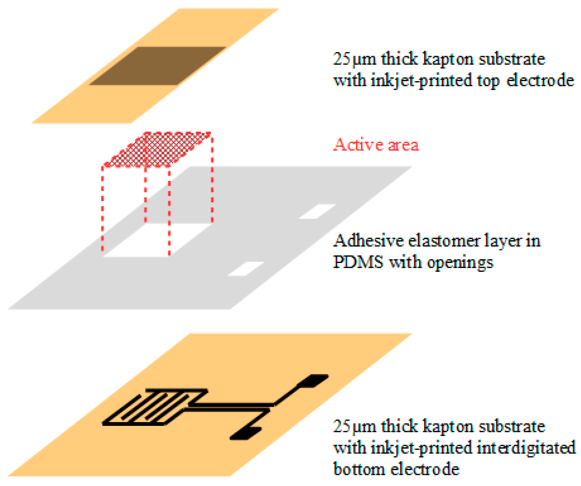
The structure and an exploded view of the force sensor are presented on the Figure 1. The manufacturing steps of the printed device are detailed below. A bottom interdigitated electrode is first printed by inkjet process on a 25 μm thick flexible substrate. A spacer is then deposited by spin-coating. This spacer is an elastomer, the polydimethylsiloxane (PDMS). An opening is created in this spacer above the bottom electrode in order to define an active area. Finally a top electrode is inkjet-printed on another 25 μm thick flexible substrate. This second substrate is turned over, lined up, and glued on the first one thanks to the adhesive properties of the elastomer layer.
The choice of the PDMS was done because of its properties: elastic, transparent, biocompatible, chemically inert, and easy to manufacture. The PDMS is elaborated from the Sylgard® 184 Silicone Elastomer kit of the Dow Corning Corporation. The two liquid components of the kit, the base and hardener, are mixed in a 10 to 1 ratio. The mixture is realized by magnetic stirring at low velocity and under suction to avoid the formation of air bubbles. A well-controlled weight of liquid PDMS is used for each deposition with the spin-coater. A preliminary study permitted to set the parameters of the spin-coater (acceleration, velocity, time of deposition) in order to get the expected thickness layer. After a thermal curing on a hot plate (100 °C during 35 min as recommended by the provider), a well flexible and stretchable elastomer layer is reached.
2.2. Inkjet Printing Process
The choice of the inkjet printing process among the printing technologies is due to the fact that is a digital, contactless, and additive process [11,12]. Its drawbacks are the sturdiness and the stability of the process. In consequence, before any printing, the substrates are cleaned by means of successive ultrasound baths. The four baths of the cleaning procedure are: liquinox, acetone, isopropanol, and ethanol. The choice of the Kapton as flexible substrate was led by its high thermal resistance.
The inkjet-printing machine is a MicroFab Jetlab4 drop-on-demand (DOD) printer with only one head fit with a 50 μm diameter nozzle. The ink ejection is controlled by a piezoelectric command. The inkjet-printing process must be optimized to get one and only one droplet, at the good distance of the substrate.
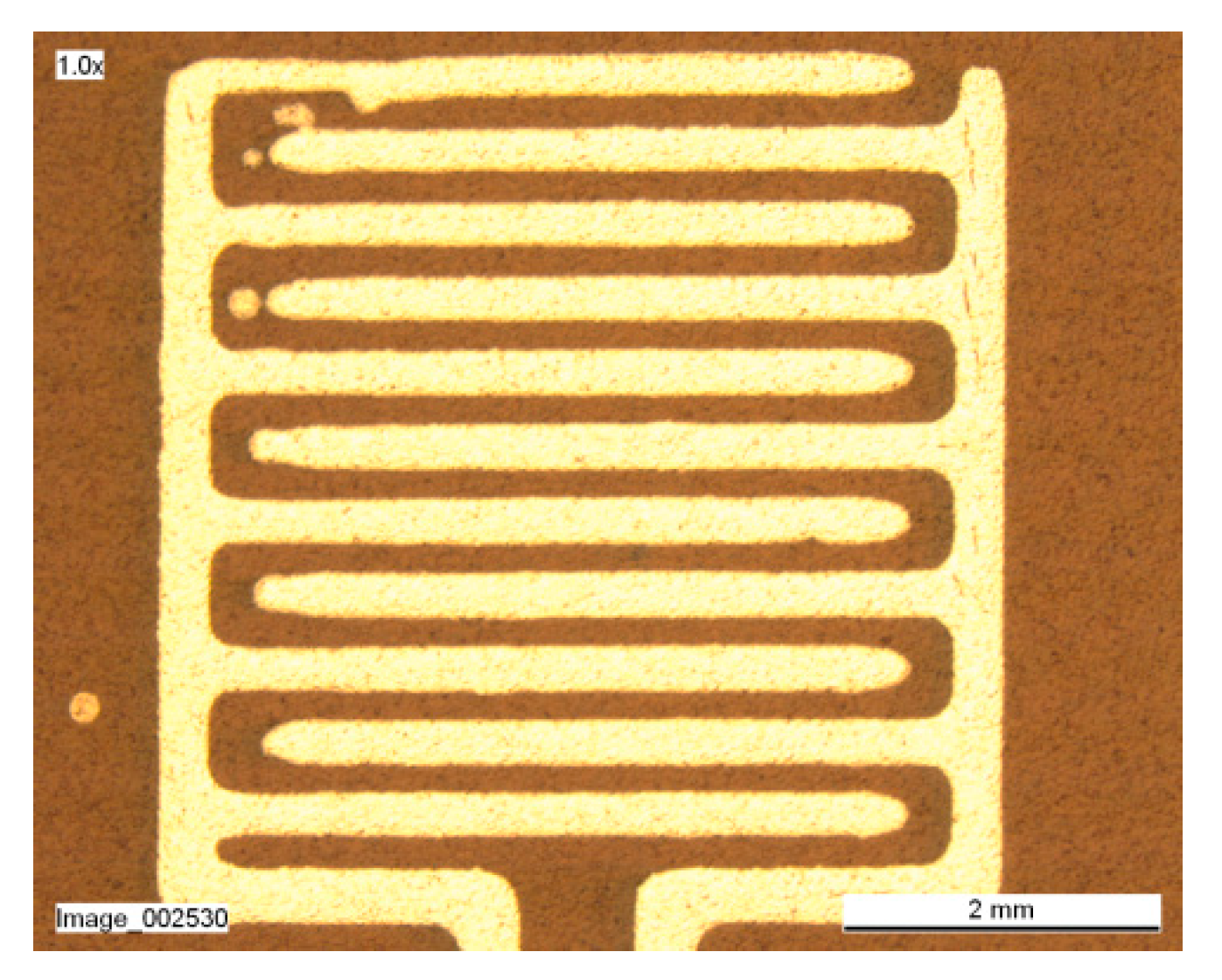
An organic silver complex compound (TEC-IJ-010 from InktecCo. Ltd., Danwon-Gu Ansan, South Korea) is used as metallic ink. Before printing, the ink is sonicated during 30 min to avoid the clogging of the nozzle. After printing, the sample is dried on a hotplate at 130 °C during 10 min in order to evacuate solvents. Then a thermal curing (in a conventional oven) is done at 150 °C during 30 min as recommended by the ink provider in order to get a high electrical conductivity of the metallic patterns. As an example, a picture of the bottom interdigitated electrode printed by inkjet process is presented on the Figure 2.
3. Results and Discussion
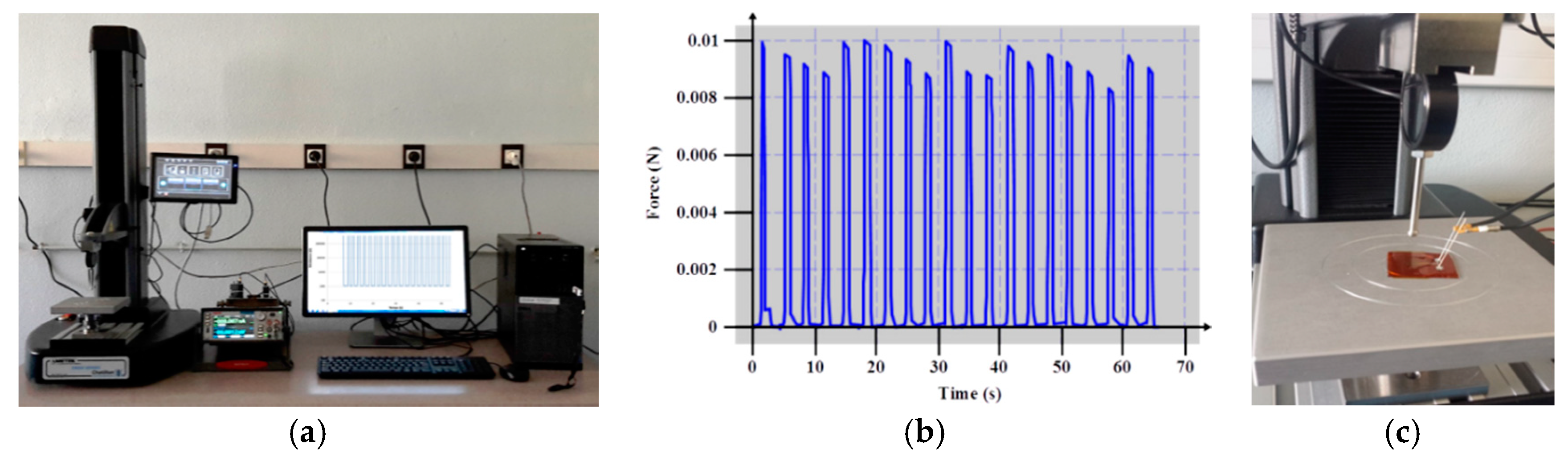
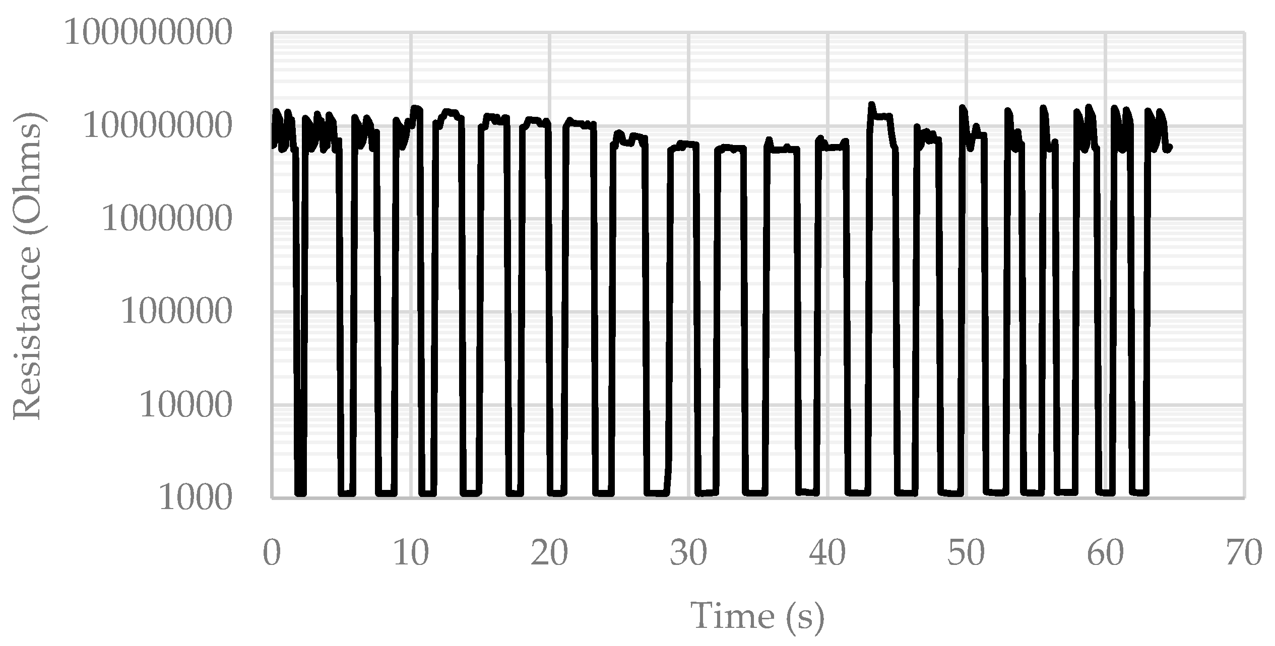
The characterization of the force sensor is realized thanks to a test bench composed of a Chatillon CS-225 digital force tester, a Keithley sourcemeter and a data acquisition system. The force is applied perpendicularly to the surface of the sensor (see Figure 3). When no force is applied, the bottom and top electrodes are not in contact, and the resistance of the sensor tends toward infinity. When an enough force is applied, the electrodes are in contact and the resistance tends to 0. Two additional series and shunt resistors (of 1 kOhms and 10 MOhms respectively) are associated to the sensor for current limitations.
The minimal actuation force needed to put in contact the electrodes is as low as 0.01 N (see Figure 3 and Figure 4). The application of the force is repeated as quickly as possible (at a frequency lower than 1 Hz) with the digital force tester for this very low force. The dynamic behavior of the force sensor is satisfactory, in the limit of the capabilities of the test bench.
4. Conclusions
A printed force sensor on flexible substrate is fabricated from only few manufacturing steps. Two electrodes (bottom and top) are printed on two different substrates (25 μm thick Kapton substrates). An elastomer layer of PDMS is fabricated by spin-coating and placed on the bottom electrode in order to be used as a spacer. An opening is created in the spacer to define an active area. The substrate of the top electrode is finally turned over, lined up, and glued on the first one thanks to the adhesive properties of the elastomer layer. The electrodes are made thanks to a silver ink and an inkjet-printer. The characterization of the force sensor has shown that the resistance of the sensor tends to 0 or infinity if a vertical force is applied or not, respectively. The actuation force is as low as 0.01N and the dynamic behavior of the sensor is satisfactory. This low-cost printed sensor could be used in ultra-low power applications as, for instance, in passive RFID tags.
Acknowledgments
This research work took place in the framework of the VEADISTA (Remote monitoring of vital parameters and smart alerts) project that was supported by the FUI13 program and Bpifrance.
Conflicts of Interest
The authors declare no conflict of interest.
References
- Park, J.W.; Shin, D.C.; Park, S.H. Large-area OLED lightings and their applications. Semicond. Sci. Technol. 2011, 26, 034002. [Google Scholar] [CrossRef]
- Hong, K.; Lee, J.L. Review paper: Recent developments in light extraction technologies of organic light emitting diodes. Electron. Mater. Lett. 2011, 7, 77–91. [Google Scholar] [CrossRef]
- Chansin, G. Printed and Flexible Sensors 2017–2027: Technologies, Players, Forecasts; IDTechEx Report; IDTechEx Ltd.: Cambridge, UK, 2016. [Google Scholar]
- Commercial Micro Manufacturing International. Available online: http://www.cmmmagazine.com/cmm-articles/printedflexible-stretchable-sensors-new-technologies-enable-/ (accessed on 4 August 2017).
- Gubbi, J.; Buyya, R.; Marusic, S.; Palaniswami, M. Internet of things (IoT): A vision, architectural elements, and future directions. Future Gener. Comput. Syst. 2013, 29, 1645–1660. [Google Scholar] [CrossRef]
- Vermesan, O.; Friess, P.; Guillemin, P.; Sundmaeker, H.; Eisenhauer, M.; Moessner, K.; Arndt, M.; Spirito, M.; Medagliani, P.; Giaffreda, R.; et al. Internet of things strategic research and innovation agenda. In Internet of Things—From Research and Innovation to Market Deployment; Vermesan, O., Friess, P., Eds.; River Publishers: Gistrup, Denmark, 2014; pp. 7–142. [Google Scholar]
- Ferdous, R.M.; Reza, A.W.; Siddiqui, M.F. Renewable energy harvesting for wireless sensors using passive RFID tag technology: A review. Renew. Sustain. Energy Rev. 2016, 58, 1114–1128. [Google Scholar] [CrossRef]
- Ando, B.; Baglio, S.; Bulsara, A.R.; Emery, T.; Marletta, V.; Pistorio, A. Low-cost inkjet printing technology for the rapid prototyping of transducers. Sensors 2017, 17, 748. [Google Scholar] [CrossRef] [PubMed]
- Correia, V.; Caparros, C.; Casellas, C.; Francesch, L.; Rocha, J.G.; Lanceros-Mendez, S. Development of inkjet-printed strain sensors. Smart Mater. Struct. 2013, 22, 105028. [Google Scholar] [CrossRef]
- Yadegari, A.; Omidi, M.; Choolaei, M.; Haghiralsadat, F.; Yazdian, F. Micro-newton detection by using graphene-paper force sensor. Procedia Eng. 2014, 87, 967–970. [Google Scholar] [CrossRef]
- Sridhar, A.; Blaudeck, T.; Baumann, R.R. Inkjet printing as a key enabling technology for printed electronics. Mater. Matters 2011, 6, 12–15. [Google Scholar]
- Singh, M.; Haverinen, H.M.; Dhagat, P.; Jabbour, G.E. Inkjet printing—Process and its applications. Adv. Mater. 2010, 22, 673–685. [Google Scholar] [CrossRef] [PubMed]
Figure 1.
Structure and exploded view of the force sensor printed on flexible substrates.

Figure 2.
Picture of the bottom interdigitated electrode printed by inkjet process.

Figure 3.
(a) Test bench permitting to apply (b) a controlled vertical force to the surface of (c) the sensor under test.
Figure 3.
(a) Test bench permitting to apply (b) a controlled vertical force to the surface of (c) the sensor under test.

Figure 4.
Electrical characterization of the inkjet-printed ON/OFF force sensor when the force described on Figure 3 is applied vertically to its surface.
Figure 4.
Electrical characterization of the inkjet-printed ON/OFF force sensor when the force described on Figure 3 is applied vertically to its surface.

Publisher’s Note: MDPI stays neutral with regard to jurisdictional claims in published maps and institutional affiliations. |
© 2017 by the authors. Licensee MDPI, Basel, Switzerland. This article is an open access article distributed under the terms and conditions of the Creative Commons Attribution (CC BY) license (https://creativecommons.org/licenses/by/4.0/).
Share and Cite
MDPI and ACS Style
Bènevent, E.; Dankoco, M.D.; Bendahan, M. Inkjet-Printed ON/OFF Force Sensor on Flexible Substrate for Ultra-Low Power Applications. Proceedings 2017, 1, 620. https://doi.org/10.3390/proceedings1040620
AMA Style
Bènevent E, Dankoco MD, Bendahan M. Inkjet-Printed ON/OFF Force Sensor on Flexible Substrate for Ultra-Low Power Applications. Proceedings. 2017; 1(4):620. https://doi.org/10.3390/proceedings1040620
Chicago/Turabian StyleBènevent, Evangéline, Mariam Dème Dankoco, and Marc Bendahan. 2017. "Inkjet-Printed ON/OFF Force Sensor on Flexible Substrate for Ultra-Low Power Applications" Proceedings 1, no. 4: 620. https://doi.org/10.3390/proceedings1040620