
The Influence of Annealing Atmosphere, Blending Ratio, and Molecular Weight on the Phase Behavior of Blend Materials


1
Integrated Circuit Advanced Process Center, Institute of Microelectronics of Chinese Academy of Sciences (IMECAS), No. 3 Beitucheng West Road, Beijing 100029, China
2
University of Chinese Academy of Sciences, No. 19(A), Yuquan Road, Beijing 100049, China
*
Authors to whom correspondence should be addressed.
Processes 2021, 9(9), 1586; https://doi.org/10.3390/pr9091586
Submission received: 16 July 2021
/
Revised: 27 August 2021
/
Accepted: 2 September 2021
/
Published: 5 September 2021
Abstract
:In the study of block copolymers, many parameters need to be adjusted to obtain good phase separation results. Based on block copolymer polystyrene-b-polycarbonate and homopolymer polystyrene, the effects of the annealing atmosphere, blending ratio, and molecular weight on phase separation were studied. The results show that annealing in air can inhibit the occurrence of phase separation. In addition, snowflake patterns are formed during phase separation. The blending ratio affects the quality of the pattern. The molecular weight affects the size of the pattern, and the size increases as the molecular weight increases. In this article, the influence of process conditions and materials on phase separation was discussed, which has laid a solid foundation for the development of block copolymer self-assembly in the future.
1. Introduction
In recent years, more and more attention has been paid to the self-assembly of block copolymers because it has great application prospects in the field of integrated circuits, biology, and many other fields. In the field of integrated circuits, nanostructures in electronic devices are fabricated by photolithography. Due to the diffraction limit of the radiation source, lithography faces inherent challenges in reducing the critical size to less than 20 nm. Thus, we need to discover a new technology to replace it. According to the international technology roadmap for semiconductors, the solutions of next-generation lithography mainly include extreme ultraviolet lithography [1,2,3], nanoimprint lithography [4,5,6], and block copolymer self-assembly [7,8]. At present, extreme ultraviolet lithography is the most widely used technology. However, its manufacturing cost is also the highest [9]. Nanoimprint requires a high-precision template, but the cost of template manufacturing is high, and the yield is limited. Block copolymer self-assembly has natural advantages over other technologies concerning cost and process. Block copolymer self-assembly can form hexagonal cylinders, cubic spheres, alternative lamellae, and bicontinuous gyroids. At the same time, the process of block copolymer self-assembly is relatively simple, which can greatly shorten the manufacturing time.
In the research into block copolymer self-assembly technology, it is necessary to constantly reduce the size of the structure and innovate the process. Nowadays, the self-assembly of block copolymers can form nanostructures of 1–100 nm [10,11]. Researchers have explored the properties of block copolymers from the material itself, such as material synthesis, from the initial binary block copolymers to the present ternary or even multivariate block copolymers. In addition, a number of research groups have explored the self-assembly of block copolymers in many ways. On the one hand, the self-assembly morphology can be adjusted by changing the components of the two blocks in the binary block copolymer. On the other hand, the self-assembly morphology can be controlled by changing the molecular weight of the block copolymer. In order to obtain rich micro-region morphology of self-assembled block copolymers, researchers control and adjust the relevant process conditions to achieve this goal. For example, a temperature field [12,13], temperature gradient field [14,15], solvent field [16,17,18,19,20], shear field [21,22,23], magnetic field [24,25,26,27,28], and electric field [29,30,31] can be applied to control the morphology of self-assembled block copolymers. Both industry and academia have conducted a great deal of research into the morphology of field-regulated block copolymers. For example, Hashimoto et al. designed a temperature gradient instrument to control the microstructure of block copolymers [15]. Kim and Libera have studied the effect of solvents on the morphology of triblock copolymer films under different evaporation rates [17]. Morkved and his colleagues first studied block copolymer films on silicon nitride films under a plane electric field [30]. Based on the temperature field, we use the experimental method of air atmosphere annealing to explore how the phase separation process will change in an air atmosphere environment. In addition, the effects of blending ratio and molecular weight on phase separation are also discussed.
In this paper, the influence of air atmosphere annealing on the self-assembly of block copolymers was investigated by using the blends of block copolymers PS-b-PC and its homopolymer PS. Compared with the results of vacuum annealing, it was found that the air atmosphere environment can inhibit the phase separation process. The results of this study are of great significance to further understand the self-assembly of new block copolymers.
2. Experiment
2.1. Materials
The material used was a block copolymer poly(styrene-b-polycarbonate) (denoted as PS-b-PC, Mn = 7000 g mol−1, PDI = 1.157, PS mole fraction = 66%, PC mole fraction = 34%) and a homopolymer polystyrene (denoted as PS, Mn = 3700 g mol−1, PDI = 1.183). PS and PC were mixed in a certain ratio to form blend materials. The material used was a random copolymer, poly(styrene-co-methylmethacrylate-co-glycidyl methacrylate) (denoted as PS-PMMA-PGMA, Mn = 10,100 g mol−1, PDI = 2.177, PS mole fraction = 52%, PMMA mole fraction = 42%, PGMA mole fraction = 6%).
The bare silicon wafer used in this study was 100 mm in diameter, with p-type doped (100) plane and approximately 1.5 nm thick native oxide. The wafer was cleaned with sulfuric acid and hydrogen peroxide mixed solution at 115 °C for 15 min, followed by ammonium hydroxide and hydrogen peroxide mixed solution at 70 °C for 15 min. Then, the wafer was rinsed with deionized water and dried under a flow of N2 to remove any organic contamination and to increase the concentration of hydroxyl groups on the surface for the graft of a neutral layer.
2.2. Preparation of Neutral Layer
PS-PMMA-PGMA solutions 0.5 wt% in propylene glycol monomethyl ether acetate (PGMEA) were spin-coated onto the cleaned wafers at 1500 rev per min for 30 s. Subsequently, the samples were annealed in an oven at 180 °C for 10 min under a vacuum atmosphere to graft the chains of PS-PMMA-PGMA onto the hydroxyl functionalized surface.
2.3. Preparation of BCP Films
PS-b-PC solutions of 1 wt% in PGMEA and PS solutions of 1 wt% in PGMEA were mixed to form blended materials. Blend material solutions were spin-coated onto the wafers at 2000 rev per min for 30 s. The wafers were annealed in an oven under a vacuum atmosphere.
2.4. Characterization
A Hitachi S-5500 scanning electron microscope (SEM) was used to collect images at an accelerating voltage of 3 kV. To obtain the original morphologies of the films, no other process such as plasma etching or metal sputtering was performed on the samples to enhance the contrast.
3. Results
3.1. Atmosphere Affects the Phase Separation
In order to accurately compare the phase separation changes of vacuum and air atmosphere, we chose the annealing temperature of 130 °C for the experiment because the morphology changes slowly with the temperature at this temperature, which is easier to compare.
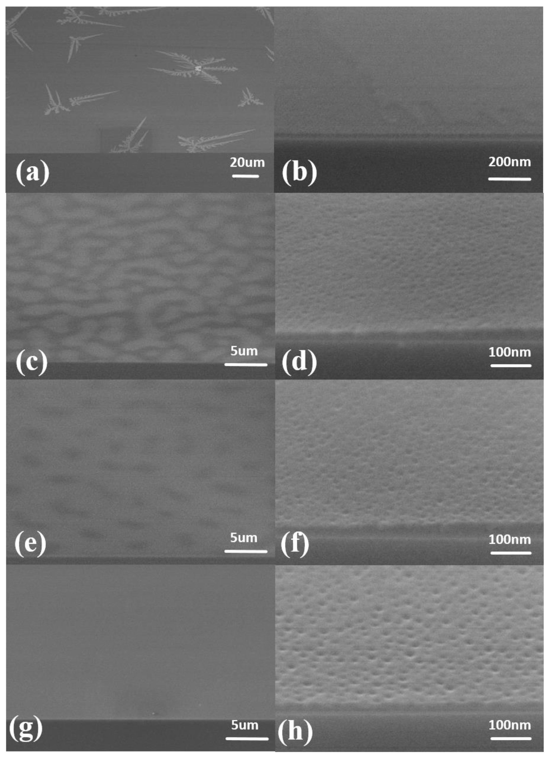
When the annealing atmosphere is air, the SEM results are as shown in Figure 1. When the annealing time was 10 min, the patterns formed in the shape of snowflakes in the SEM image (Figure 1a). No cylinders were formed in the film (Figure 1b). Increasing the annealing time to 20 min, the snowflake pattern changed to a block pattern (Figure 1c). At this time, patterned microdomains began to form (Figure 1d). When the annealing time was 30 min, the white block pattern disappeared into a black spot (Figure 1e), and the cylinders rose in number (Figure 1f). In addition, as the annealing time was 40 min, there was no special pattern on the surface of the thin film (Figure 1g). The formation of a regular cylindrical structure can be clearly observed (Figure 1h).
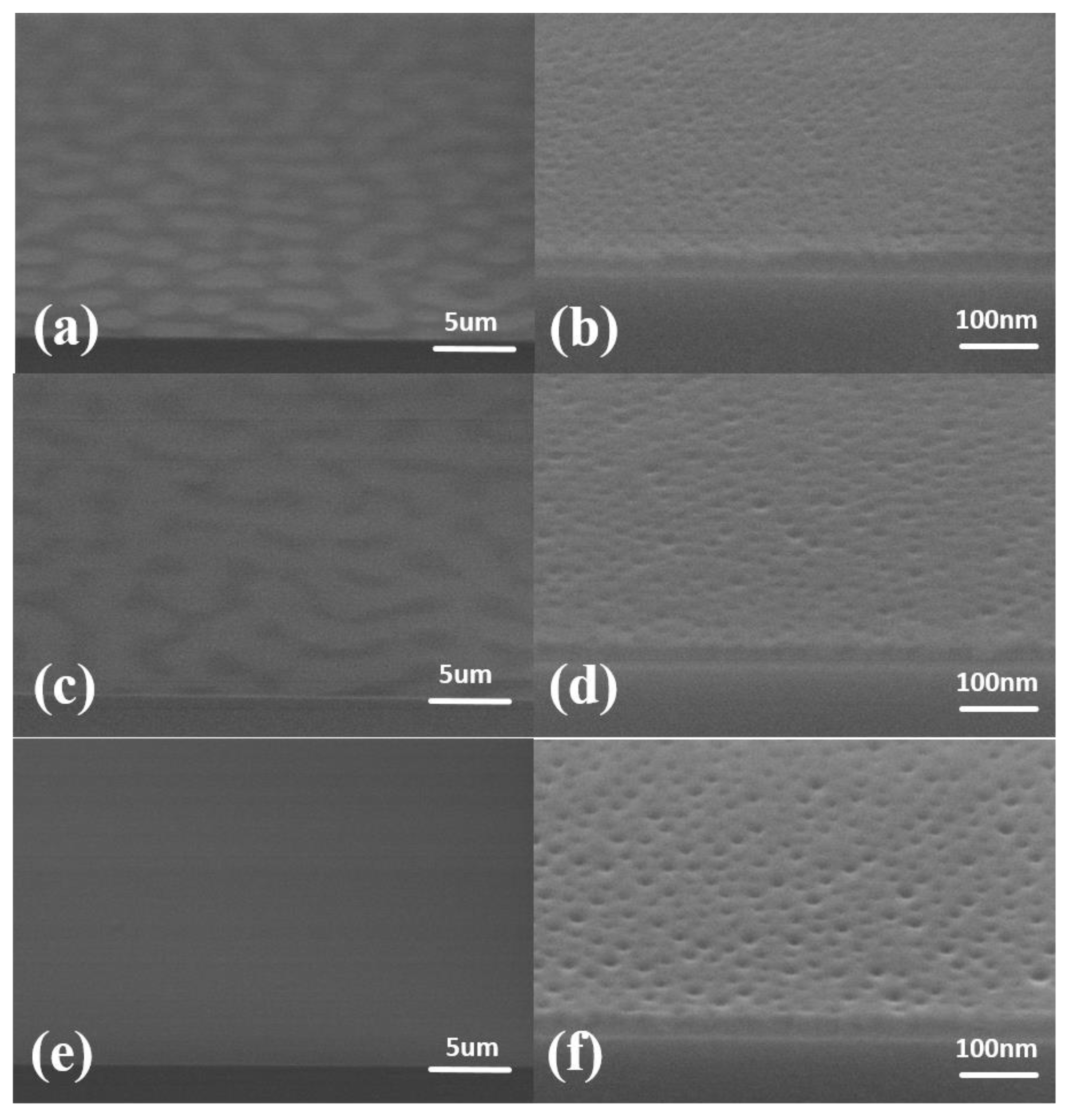
When the annealing atmosphere was a vacuum, the SEM results are as shown in Figure 2. When the annealing time was 10 min, the SEM showed a white block pattern (Figure 2a). At this time, the cylinders have formed (Figure 2b). After increasing the annealing time to 20 min, the white block pattern disappeared into black spots (Figure 2c). The number of cylinders increased (Figure 2d). As the annealing time was 30 min, there was no special pattern on the surface of the film (Figure 2e). The formation of a regular cylindrical structure can be clearly observed (Figure 2f).
Comparing the two experimental results, we found that there are different experimental phenomena between vacuum annealing and air annealing. Annealing in a vacuum atmosphere will cause the formation of white spots. While annealing in an air atmosphere, in addition to the formation of white spots, there will also be the formation of snowflake-like patterns. In addition, annealing in an air atmosphere takes longer to reach a stable structure of phase separation.
It is believed that the air atmosphere will lead to slower evaporation of the residual solvent. This is the main reason for the formation of snowflake-like structures and inhibition of the phase separation process.
3.2. Ratio Affects the Phase Separation
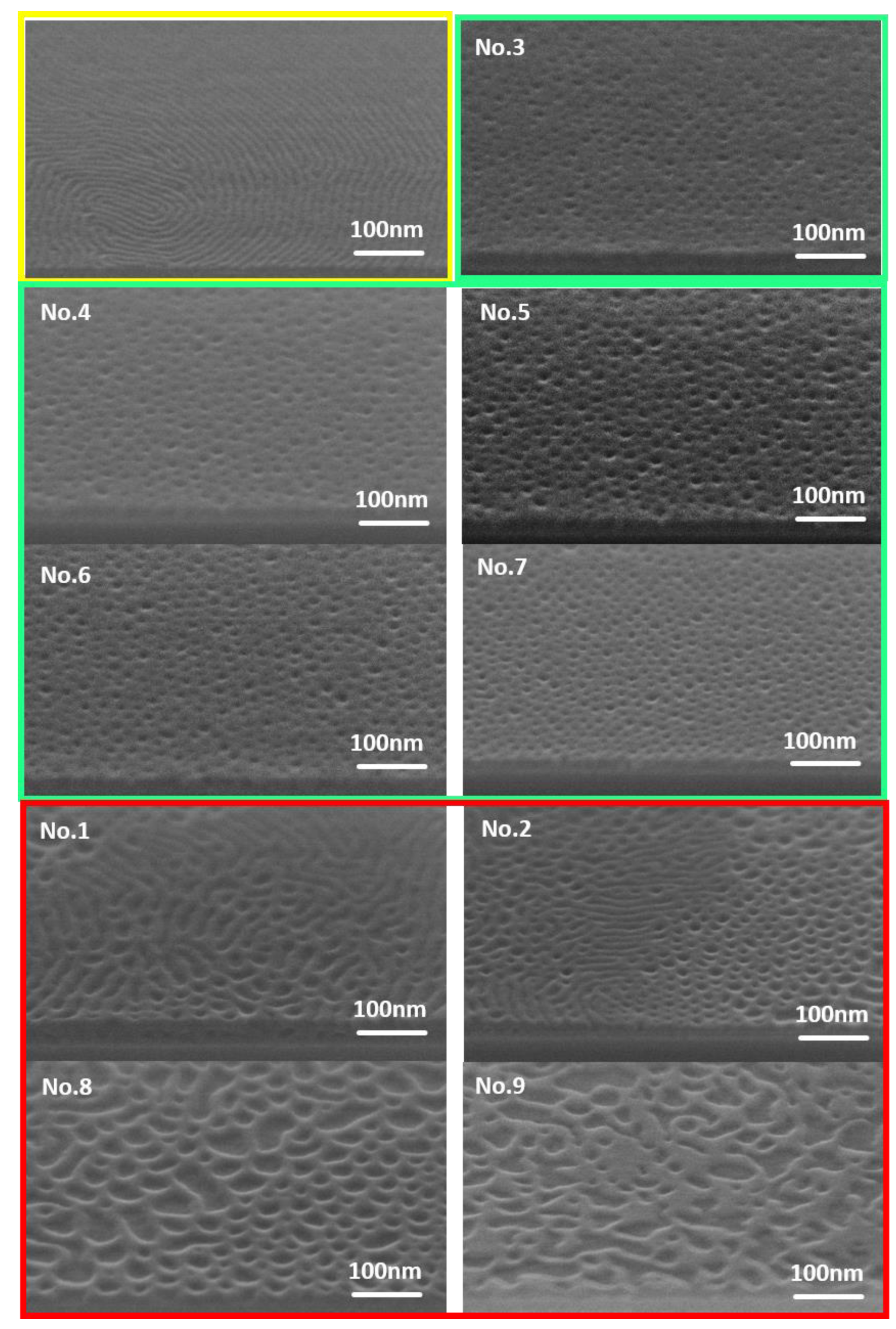
In order to explore the controllability of the blend ratio of PS-b-PC to PS, we designed nine groups of experiments (Table 1, in which the ratio of PS-b-PC to PS is the volume ratio). Experiment results are shown in Figure 3, in which the annealing temperature is 130 °C, the annealing time is 30 min, and the annealing atmosphere is a vacuum. Different sub-figures represent different blend ratios. Experimental results showed that cylindrical structures could be formed when the PS-b-PC to PS ratio is from 2.5:1 to 1:1.5 (experimental No. 3 to No. 7). Outside this range, cylinder cannot be formed, but there are other patterns.
In Figure 3, the yellow box is the layered structure formed by the phase separation of pure PS-b-PC; the pitch of lamellar is about 16 nm. The green box is the columnar structure formed by the phase separation of the blended material corresponding to experiments No. 3 to No. 7, in which the cylinder diameters are 12.36 nm, 13.09 nm, 15.12 nm, 14.26 nm, and 11.85 nm, respectively. The red boxes are other structures formed by the phase separation of the blended materials, in which experiments No. 1 and No. 2 formed a mixed structure of layered and porous, and experiments No. 8 and No. 9 formed irregular structures.
When the proportion of PS is low, layered and porous structures are formed. With an increase in the PS ratio, the microdomain area of the layered structure decreases, and the microdomain area of the porous structure increases. When PS-b-PC:PS reaches 2.5:1, self-assembly forms a columnar structure. When PS-b-PC:PS is 1:2, the structure becomes irregular.
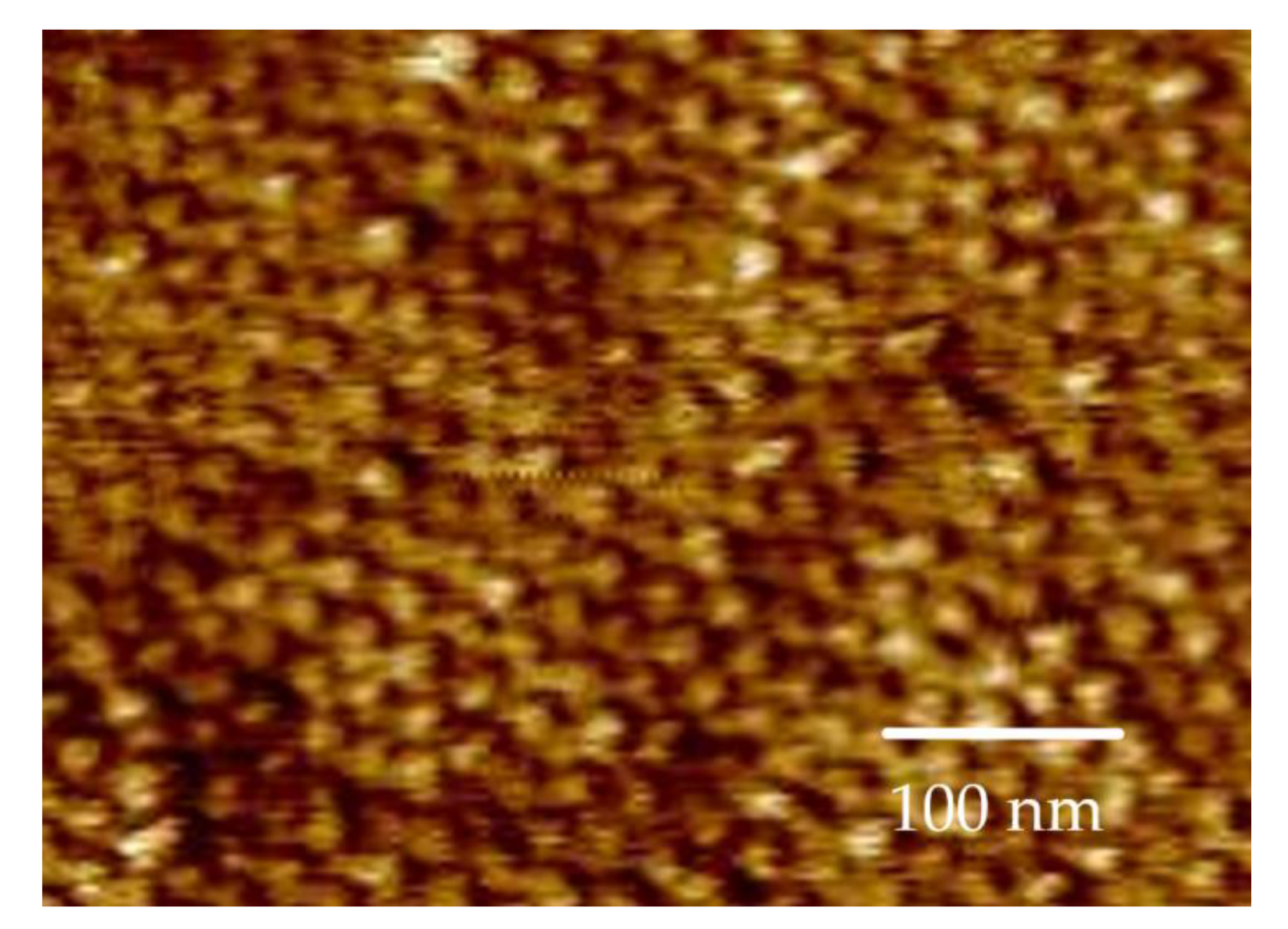
Figure 4 showed that the formation of the pattern is, in fact, cylinders.
3.3. Molecular Weight Affects the Phase Separation
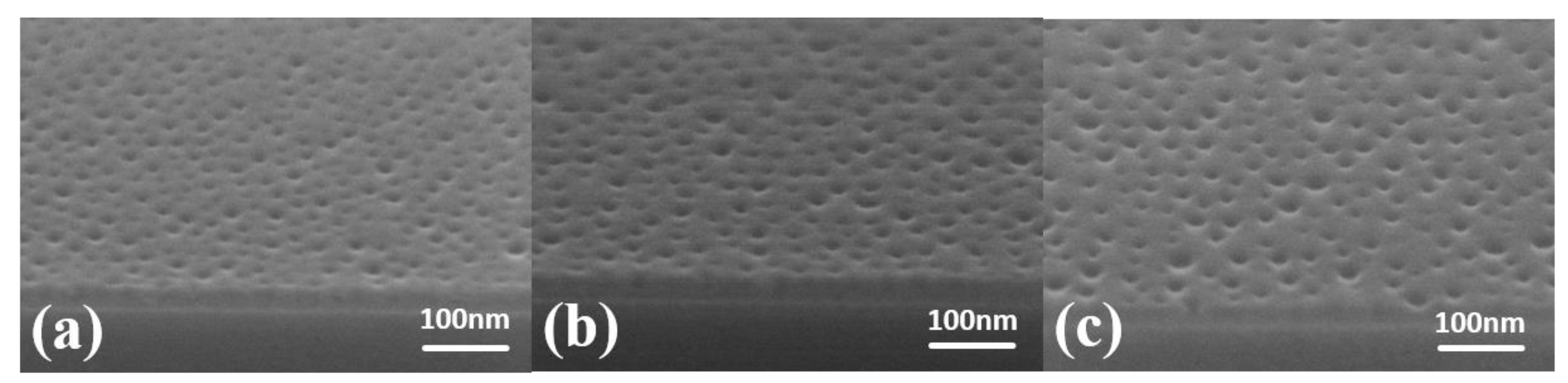
The influence of the molecular weight of the block copolymer on the quality of phase separation pattern was explored. Two new samples, samples 2 and 3, were added to the experiment, as shown in Table 2. Experiments showed that with an increase in molecular weight, the size of the cylinder increased (Figure 5). By comparing Figure 5a with Figure 5c, the results showed that the spacing between cylinders increased.
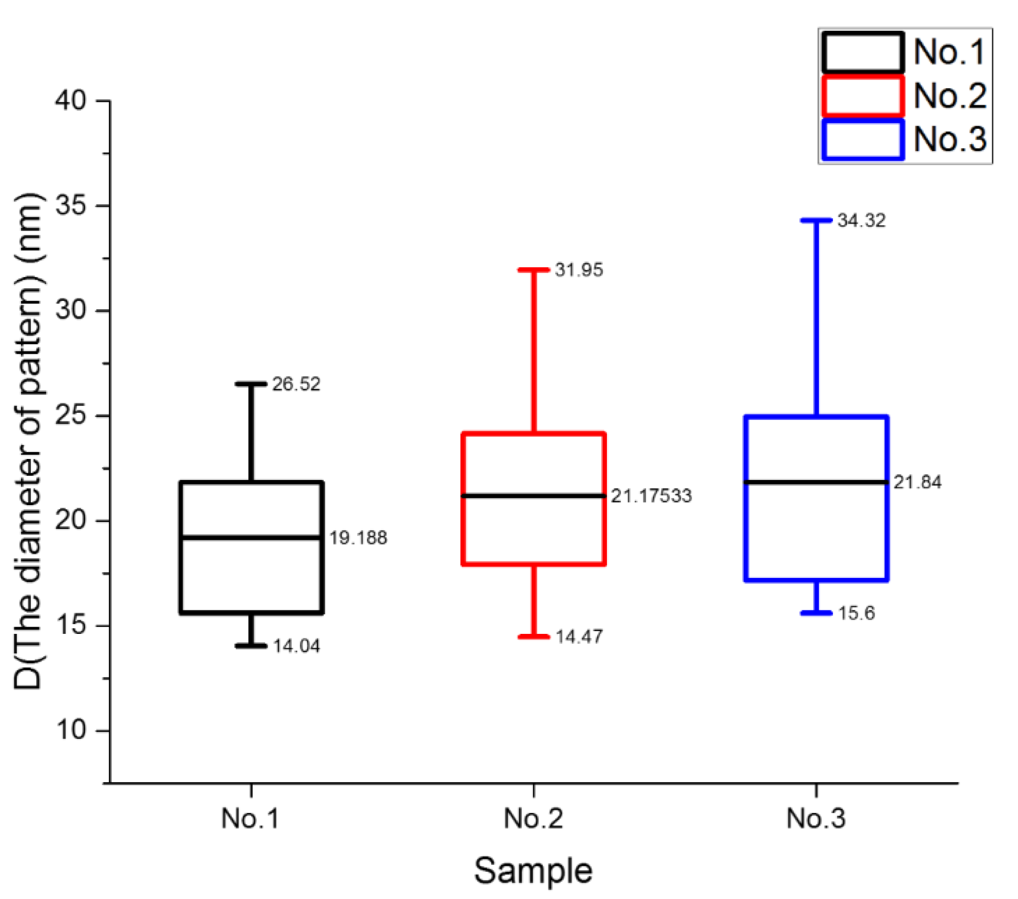
In order to reflect the experimental results more accurately, we collected and calculated the data extracted from the SEM images and plotted the result, as shown in Figure 5. The diameter of the structures was used to describe the dynamic process. Figure 6 shows the pattern diameters of the samples with different molecular weights. The average diameters of sample 1, sample 2, and sample 3 were 19.188 nm, 21.17533 nm, and 21.84 nm, respectively. With an increase in molecular weight, the size of the pattern increased but the pattern structure became sparse.
4. Discussion
Through the above experiments, we found that not only does the annealing atmosphere affect the quality of the phase separation but also the molecular weight and blending ratio of the material. For the application of self-assembly technology to semiconductor technology, vacuum annealing can shorten the annealing time compared with air annealing, which can greatly reduce the process cost. In addition, by adjusting the ratio of block copolymer to homopolymer, a variety of morphologies can be formed. The controllability of the ratio makes it possible to form different semiconductor structures. In the experiment, the size of the pattern increased as the molecular weight increased. For different semiconductor nodes, block copolymers of different molecular weights could be used. This has laid a solid foundation for exploring the development of blend materials.
5. Conclusions
In this paper, the influence of process conditions and material parameters on phase behavior was explored. By comparing the results of annealing in a vacuum atmosphere and air atmosphere, it was found that the air atmosphere inhibits the phase separation process and is accompanied by the formation of snowflake-like patterns. In terms of blending ratio, the ratio of block copolymer to homopolymer needs to be adjusted to achieve the desired phase separation result. The molecular weight of the block copolymer is also an important influencing factor. That is, different cylinder sizes could be formed by adjusting the molecular weight, which can be applied to different nodes in the semiconductor process. In addition, the space dimension could also be controlled by adjusting the molecular weight, which is useful for the pattern grouping process during IC manufacturing. In summary, the pattern quality is determined by the annealing atmosphere, blending ratio, and molecular weight. In the future, we will continue to explore the impact of new factors on pattern quality.
Author Contributions
Writing—original draft preparation, formal analysis, investigation, methodology, W.L.; format analysis, methodology, writing—review and editing, L.Z.; methodology, funding acquisition, supervision, Y.W. All authors have read and agreed to the published version of the manuscript.
Funding
This research was funded by the National Key Research and Development Program of China, grant number 2017YFA0206002, and partially supported by the National Science and Technology Major Project of China, grant number 2017ZX02315001-003.
Institutional Review Board Statement
Not applicable.
Informed Consent Statement
Not applicable.
Data Availability Statement
Not applicable.
Acknowledgments
The authors would like to thank the support of the Key Laboratory of Microelectronics Devices and Integrated Technology of CAS.
Conflicts of Interest
There are no conflicts to declare.
References
- Kemp, K.; Wurm, S. EUV lithography. Comptes Rendus Phys. 2006, 7, 875–886. [Google Scholar] [CrossRef]
- Putna, E.S.; Younkin, T.R.; Caudillo, R.; Chandhok, M. EUV lithography for 22nm half pitch and beyond: Exploring resolution, LWR, and sensitivity tradeoffs. In Proceedings of the Extreme Ultraviolet (EUV) Lithography, San Jose, CA, USA, 22–25 February 2010. p. 76360P. [Google Scholar]
- Päivänranta, B.; Langner, A.; Kirk, E.; David, C.; Ekinci, Y. Sub-10 nm patterning using EUV interference lithography. Nanotechnology 2011, 22, 375302. [Google Scholar] [CrossRef]
- Lee, H.; Jung, G.-Y. Full wafer scale near zero residual nano-imprinting lithography using UV curable monomer solution. Microelectron. Eng. 2005, 77, 42–47. [Google Scholar] [CrossRef]
- Guo, L.J. Nanoimprint lithography: Methods and material requirements. Adv. Mater. 2007, 19, 495–513. [Google Scholar] [CrossRef] [Green Version]
- Byeon, K.-J.; Lee, H. Recent progress in direct patterning technologies based on nano-imprint lithography. Eur. Phys. J. Appl. Phys. 2012, 59, 10001. [Google Scholar] [CrossRef] [Green Version]
- Hawker, C.J.; Russell, T.P. Block copolymer lithography: Merging “bottom-up” with “top-down” processes. MRS Bull. 2005, 30, 952–966. [Google Scholar] [CrossRef] [Green Version]
- Ruiz, R.; Kang, H.; Detcheverry, F.A.; Dobisz, E.; Kercher, D.S.; Albrecht, T.R.; de Pablo, J.J.; Nealey, P.F. Density multiplication and improved lithography by directed block copolymer assembly. Science 2008, 321, 936–939. [Google Scholar] [CrossRef]
- Wagner, C.; Harned, N. Lithography gets extreme. Nat. Photonics 2010, 4, 24–26. [Google Scholar] [CrossRef]
- Qiang, X.; Chakroun, R.; Janoszka, N.; Gröschel, A.H. Self-assembly of Multiblock Copolymers. Isr. J. Chem. 2019, 59, 945–958. [Google Scholar] [CrossRef]
- Jeong, J.W.; Park, W.I.; Do, L.M.; Park, J.H.; Kim, T.H.; Chae, G.; Jung, Y.S. Nanotransfer Printing with sub-10 nm Resolution Realized using Directed Self-Assembly. Adv. Mater. 2012, 24, 3526–3531. [Google Scholar] [CrossRef]
- Banaszak, M.; Wołoszczuk, S.; Jurga, S.; Pakula, T. Lamellar ordering in computer-simulated block copolymer melts by a variety of thermal treatments. J. Chem. Phys. 2003, 119, 11451–11457. [Google Scholar] [CrossRef]
- Albalak, R.J.; Thomas, E.L.; Capel, M.S. Thermal annealing of roll-cast triblock copolymer films. Polymer 1997, 38, 3819–3825. [Google Scholar] [CrossRef]
- Hashimoto, T.; Yamauchi, K.; Yamaguchi, D.; Hasegawa, H. Competing short-range and long-range interactions in block copolymers: A role of connectivity in polymer science. Macromol. Symp. 2003, 201, 65–76. [Google Scholar] [CrossRef]
- Bodycomb, J.; Funaki, Y.; Kimishima, K.; Hashimoto, T. Single-grain lamellar microdomain from a diblock copolymer. Macromolecules 1999, 32, 2075–2077. [Google Scholar] [CrossRef]
- Kim, G.; Libera, M. Morphological development in solvent-cast polystyrene−polybutadiene−polystyrene (SBS) triblock copolymer thin films. Macromolecules 1998, 31, 2569–2577. [Google Scholar] [CrossRef]
- Son, J.G.; Chang, J.-B.; Berggren, K.K.; Ross, C.A. Assembly of sub-10-nm block copolymer patterns with mixed morphology and period using electron irradiation and solvent annealing. Nano Lett. 2011, 11, 5079–5084. [Google Scholar] [CrossRef]
- Kimura, M.; Misner, M.J.; Xu, T.; Kim, S.H.; Russell, T.P. Long-range ordering of diblock copolymers induced by droplet pinning. Langmuir 2003, 19, 9910–9913. [Google Scholar] [CrossRef]
- Kim, S.H.; Misner, M.J.; Russell, T.P. Solvent-induced ordering in thin film diblock copolymer/homopolymer mixtures. Adv. Mater. 2004, 16, 2119–2123. [Google Scholar] [CrossRef]
- Bai, W.; Yager, K.; Ross, C. In situ characterization of the self-assembly of a polystyrene–polydimethylsiloxane block copolymer during solvent vapor annealing. Macromolecules 2015, 48, 8574–8584. [Google Scholar] [CrossRef]
- Villar, M.A.; Rueda, D.R.; Ania, F.; Thomas, E.L. Study of oriented block copolymers films obtained by roll-casting. Polymer 2002, 43, 5139–5145. [Google Scholar] [CrossRef]
- Koppi, K.A.; Tirrell, M.; Bates, F.S. Shear-induced isotropic-to-lamellar transition. Phys. Rev. Lett. 1993, 70, 1449. [Google Scholar] [CrossRef] [PubMed]
- Riise, B.L.; Fredrickson, G.H.; Larson, R.G.; Pearson, D.S. Rheology and shear-induced alignment of lamellar diblock and triblock copolymers. Macromolecules 1995, 28, 7653–7659. [Google Scholar] [CrossRef]
- Majewski, P.W.; Gopinadhan, M.; Osuji, C.O. Magnetic field alignment of block copolymers and polymer nanocomposites: Scalable microstructure control in functional soft materials. J. Polym. Sci. Part B Polym. Phys. 2012, 50, 2–8. [Google Scholar] [CrossRef]
- Ferri, D.; Wolff, D.; Springer, J.; Francescangeli, O.; Laus, M.; Angeloni, A.S.; Galli, G.; Chiellini, E. Phase and orientational behaviors in liquid crystalline main-chain/side-group block copolymers. J. Polym. Sci. Part B Polym. Phys. 1998, 36, 21–29. [Google Scholar] [CrossRef]
- Gopinadhan, M.; Majewski, P.W.; Choo, Y.; Osuji, C.O. Order-disorder transition and alignment dynamics of a block copolymer under high magnetic fields by in situ x-ray scattering. Phys. Rev. Lett. 2013, 110, 078301. [Google Scholar] [CrossRef] [Green Version]
- Gopinadhan, M.; Majewski, P.W.; Osuji, C.O. Facile alignment of amorphous poly (ethylene oxide) microdomains in a liquid crystalline block copolymer using magnetic fields: Toward ordered electrolyte membranes. Macromolecules 2010, 43, 3286–3293. [Google Scholar] [CrossRef]
- Majewski, P.W.; Gopinadhan, M.; Jang, W.-S.; Lutkenhaus, J.L.; Osuji, C.O. Anisotropic ionic conductivity in block copolymer membranes by magnetic field alignment. J. Am. Chem. Soc. 2010, 132, 17516–17522. [Google Scholar] [CrossRef] [PubMed]
- Amundson, K.; Helfand, E.; Davis, D.D.; Quan, X.; Patel, S.S.; Smith, S.D. Effect of an electric field on block copolymer microstructure. Macromolecules 1991, 24, 6546–6548. [Google Scholar] [CrossRef]
- Morkved, T.; Lu, M.; Urbas, A.; Ehrichs, E.; Jaeger, H.; Mansky, P.; Russell, T. Local control of microdomain orientation in diblock copolymer thin films with electric fields. Science 1996, 273, 931–933. [Google Scholar] [CrossRef]
- Olszowka, V.; Hund, M.; Kuntermann, V.; Scherdel, S.; Tsarkova, L.; Boker, A. Electric field alignment of a block copolymer nanopattern: Direct observation of the microscopic mechanism. ACS Nano 2009, 3, 1091–1096. [Google Scholar] [CrossRef] [PubMed]
Figure 1.
SEM images of air atmosphere annealing. The thickness of blend materials is about 20 nm. The annealing temperature is 130 °C, and the annealing time is different: (a,b) 10 min; (c,d) 20 min; (e,f) 30 min; (g,h) 40 min.
Figure 1.
SEM images of air atmosphere annealing. The thickness of blend materials is about 20 nm. The annealing temperature is 130 °C, and the annealing time is different: (a,b) 10 min; (c,d) 20 min; (e,f) 30 min; (g,h) 40 min.

Figure 2.
SEM images of vacuum atmosphere annealing. The thickness of blend materials is about 20 nm. The annealing temperature is 130 °C, and the annealing time is different: (a,b) 10 min; (c,d) 20 min; (e,f) 30 min. The vacuum degree is −0.1 MPa.
Figure 2.
SEM images of vacuum atmosphere annealing. The thickness of blend materials is about 20 nm. The annealing temperature is 130 °C, and the annealing time is different: (a,b) 10 min; (c,d) 20 min; (e,f) 30 min. The vacuum degree is −0.1 MPa.

Figure 3.
SEM images of blend phase separation results. The annealing temperature is 130 °C, and the annealing time is 30 min. The thickness of blend materials is about 20 nm. The vacuum degree is −0.1 MPa.
Figure 3.
SEM images of blend phase separation results. The annealing temperature is 130 °C, and the annealing time is 30 min. The thickness of blend materials is about 20 nm. The vacuum degree is −0.1 MPa.

Figure 4.
AFM image of cylinders (corresponding to Figure 3 No. 7).
Figure 4.
AFM image of cylinders (corresponding to Figure 3 No. 7).

Figure 5.
SEM images of blends materials phase separation results. The annealing temperature is 130 ℃, and the annealing time is 30 min: (a) sample no. 1; (b) sample no. 2; (c) sample no. 3. The vacuum degree is −0.1 MPa.
Figure 5.
SEM images of blends materials phase separation results. The annealing temperature is 130 ℃, and the annealing time is 30 min: (a) sample no. 1; (b) sample no. 2; (c) sample no. 3. The vacuum degree is −0.1 MPa.

Figure 6.
Box diagram of cylinder diameter for different samples.


Table 1.
The experiment with different ratios.
| Experiment No. | PS-b-PC | Homopolymer(PS) |
|---|---|---|
| 1 | 3.5 | 1 |
| 2 | 3 | 1 |
| 3 | 2.5 | 1 |
| 4 | 2 | 1 |
| 5 | 1.5 | 1 |
| 6 | 1 | 1 |
| 7 | 1 | 1.5 |
| 8 | 1 | 2 |
| 9 | 1 | 2.5 |
Table 2.
The parameters of materials.
| Sample (PS-b-PC) No. | Mn (g/mol) | MW (g/mol) | PDI |
|---|---|---|---|
| 1 | 7000 | 8100 | 1.157 |
| 2 | 11,700 | 13,600 | 1.162 |
| 3 | 15,100 | 17,000 | 1.125 |
Publisher’s Note: MDPI stays neutral with regard to jurisdictional claims in published maps and institutional affiliations. |
© 2021 by the authors. Licensee MDPI, Basel, Switzerland. This article is an open access article distributed under the terms and conditions of the Creative Commons Attribution (CC BY) license (https://creativecommons.org/licenses/by/4.0/).
Share and Cite
MDPI and ACS Style
Liu, W.; Zhang, L.; Wei, Y. The Influence of Annealing Atmosphere, Blending Ratio, and Molecular Weight on the Phase Behavior of Blend Materials. Processes 2021, 9, 1586. https://doi.org/10.3390/pr9091586
AMA Style
Liu W, Zhang L, Wei Y. The Influence of Annealing Atmosphere, Blending Ratio, and Molecular Weight on the Phase Behavior of Blend Materials. Processes. 2021; 9(9):1586. https://doi.org/10.3390/pr9091586
Chicago/Turabian StyleLiu, Weichen, Libin Zhang, and Yayi Wei. 2021. "The Influence of Annealing Atmosphere, Blending Ratio, and Molecular Weight on the Phase Behavior of Blend Materials" Processes 9, no. 9: 1586. https://doi.org/10.3390/pr9091586
Note that from the first issue of 2016, this journal uses article numbers instead of page numbers. See further details here.