Article

Preparation of 2D Periodic Nanopatterned Arrays through Vertical Vibration-Assisted Convective Deposition for Application in Metal-Enhanced Fluorescence

by
Kittidhaj Dhanasiwawong
1,
Kheamrutai Thamaphat
1,2,*,
Mati Horprathum
3,
Annop Klamchuen
4,
Apiwat Phetsahai
2 and
Pichet Limsuwan
2
1
Nanoscience and Nanotechnology Graduated Program, Faculty of Science, King Mongkut’s University of Technology Thonburi, Bangkok 10140, Thailand
2
Green Synthesis and Application Laboratory, Applied Science and Engineering for Social Solution Research Unit, Department of Physics, Faculty of Science, King Mongkut’s University of Technology, Bangkok 10140, Thailand
3
National Electronics and Computer Technology Center (NECTEC), National Science and Technology Agency (NSTDA), Pathum Thani 12120, Thailand
4
National Nanotechnology Center (NANOTEC), National Science and Technology Development Agency (NSTDA), Pathum Thani 12120, Thailand
*
Author to whom correspondence should be addressed.
Processes 2022, 10(2), 202; https://doi.org/10.3390/pr10020202
Submission received: 12 December 2021 / Revised: 4 January 2022 / Accepted: 17 January 2022 / Published: 21 January 2022
(This article belongs to the Special Issue Synthesis, Characterization, and Application of Functional Materials)

Abstract

:
The performance of a metal-enhanced fluorescence (MEF) substrate is fundamentally based on the orientation of the metal nanostructures on a solid substrate. In particular, two-dimensional (2D) periodic metallic nanostructures exhibit a strong confinement of the electric field between adjacent nanopatterns due to localized surface plasmon resonance (LSPR), leading to stronger fluorescence intensity enhancement. The use of vertical vibration-assisted convective deposition, a novel, simple, and highly cost-effective technique for preparing the 2D periodic nanostructure of colloidal particles with high uniformity, was therefore proposed in this work. The influences of vertical vibration amplitude and frequency on the structure of thin colloidal film, especially its uniformity, monolayer, and hexagonal close-packed (HCP) arrangement, were also investigated. It was found that the vibration amplitude affected film uniformity, whereas the vibration frequency promoted the colloidal particles to align themselves into defect-free HCP nanostructures. Furthermore, the results showed that the self-assembled 2D periodic arrays of monodisperse colloidal particles were employed as an excellent template for a Au thin-film coating in order to fabricate an efficient MEF substrate. The developed MEF substrate provided a strong plasmonic fluorescence enhancement, with a detection limit for rhodamine 6G as low as 10−9 M. This novel approach could be advantageous in further applications in the area of plasmonic sensing platforms.

1. Introduction

Fluorescence spectroscopy is an analytical method based on an emission property of either single fluorescent molecule (fluorophore) that is triggered by the absorption of excitation radiation at a particular wavelength. It is widely used in tremendous applications in medical, life science, and biotechnology fields due to its rapid, non-destructive, and sensitive analytical method for the analysis of biomolecular substances [1]. In order to detect a target biomolecular substance, the fluorophore is particularly immobilized on the biomolecule for employment as a fluorescent probe. However, its detection of fluorescent probes at a very low concentration is limited in many cases. Therefore, the methods to achieve a strong fluorescence intensity have been intensely investigated for improving sensitivity and lowering the detection limit of bioanalytical sensors [2]. Among them, a recognized powerful technology called metal-enhanced fluorescence (MEF) is an area of particular focus, due to its ability to significantly enhance the fluorescence signal in the near-field and shield fluorophores against photobleaching processes [3,4].
The MEF technique utilizes the nanostructures of noble metals such as silver (Ag), gold (Au), and copper (Cu), or bimetallic materials such as Au-Ag, Al-Au, and Au-Cu, occupying the localized surface plasmon effect and the plasmon effect due to non-radiative interactions. The intrinsic lifetime [5] is also used to improve the performance of the MEF substrate [6,7,8]. Localized surface plasmon resonance (LSPR) is the oscillation of free electrons confined at the metal surface when the incident lights interact with the metallic nanostructures, leading to the generation of a highly concentrated local electromagnetic field near them, which results in the significant enhancement of fluorescence intensity by several orders of magnitude [9]. Many reports suggest that the MEF phenomenon depends on the morphology of the metal nanostructure, for example, its particle shape, particle size, inter-particle distance, and nano-array pattern [9,10].
Since two-dimensional (2D) ordered arrays of metallic nanostructures generate a strongly confined electric field (called a “hotspot”) in spaces between particles [11,12], various methods for the preparation of 2D periodic nanostructures, such as nano imprint [13], laser interference lithography [14], electron-beam lithography [15], and colloidal lithography [16,17], have been incessantly developed to fabricate the nanopatterned arrays, which are used as templates for the deposition of metallic materials to achieve an MEF substrate eventually. Consequently, the selection of a technique to fabricate nanopatterned arrays becomes a crucial factor affecting the performance of an MEF substrate [18].
It has been reported that the hexagonal close-packed (HCP) nanostructure that is formed through colloidal lithography techniques can be used as a template for preparing a highly efficient MEF substrate due to its tunable LSPR field [19]. Among several colloidal lithography techniques [16,20,21,22,23], convective deposition has gained much interest because of its simplicity, rapidness, and relatively low cost. It is a well-known technique for the convective self-assembly of colloidal nanospheres during solvent evaporation and consequent formation of a thin film with closed-packed structures using convective steering and capillary interaction [24,25]. However, some persistent problems associated with controlling the film’s uniformity and defects, including a non-close-packed structure, dislocation, and void, have occurred frequently [26]. Therefore, many researchers have attempted to improve the hexagonal close-packing density and the film uniformity of 2D periodic nanopatterns by adding a surfactant to reduce the surface tension of a solvent, simultaneously introducing the co-assembly of large and small colloidal particles of different sizes [27,28,29,30], or simultaneously applying mechanical vibration in the lateral direction to the deposition process, using a piezo-electric transducer [27,28]. Although these techniques can overcome the dramatic latency issues of the convective deposition technique, they require complicated steps and expensive apparatuses [27,28,29,30].
Therefore, this work proposed a novel convective deposition method without the presence of any surfactant to prepare a better 2D periodically nanopatterned film with high uniformity and lower defect density. The vertical vibration-assisted blade deposition set was developed using a local and cost-effective apparatus. The effects of vertical vibration amplitude and frequency on the uniformity, monolayer, and HCP arrangement of nanopatterned arrays, were also examined to find the optimum condition for achieving the high surface coverage of a self-assembled colloidal monolayer on a substrate. Furthermore, the 2D periodic nanopatterned arrays prepared under the optimum condition were used as a template for coating the Au thin film, using the sputtering technique to prepare the MEF substrate. Practical use of the fabricated MEF substrate to enhance the fluorescence intensity of the standard fluorescent dyes, such as rhodamine 6G (R6G), was demonstrated as well.

2. Materials and Methods

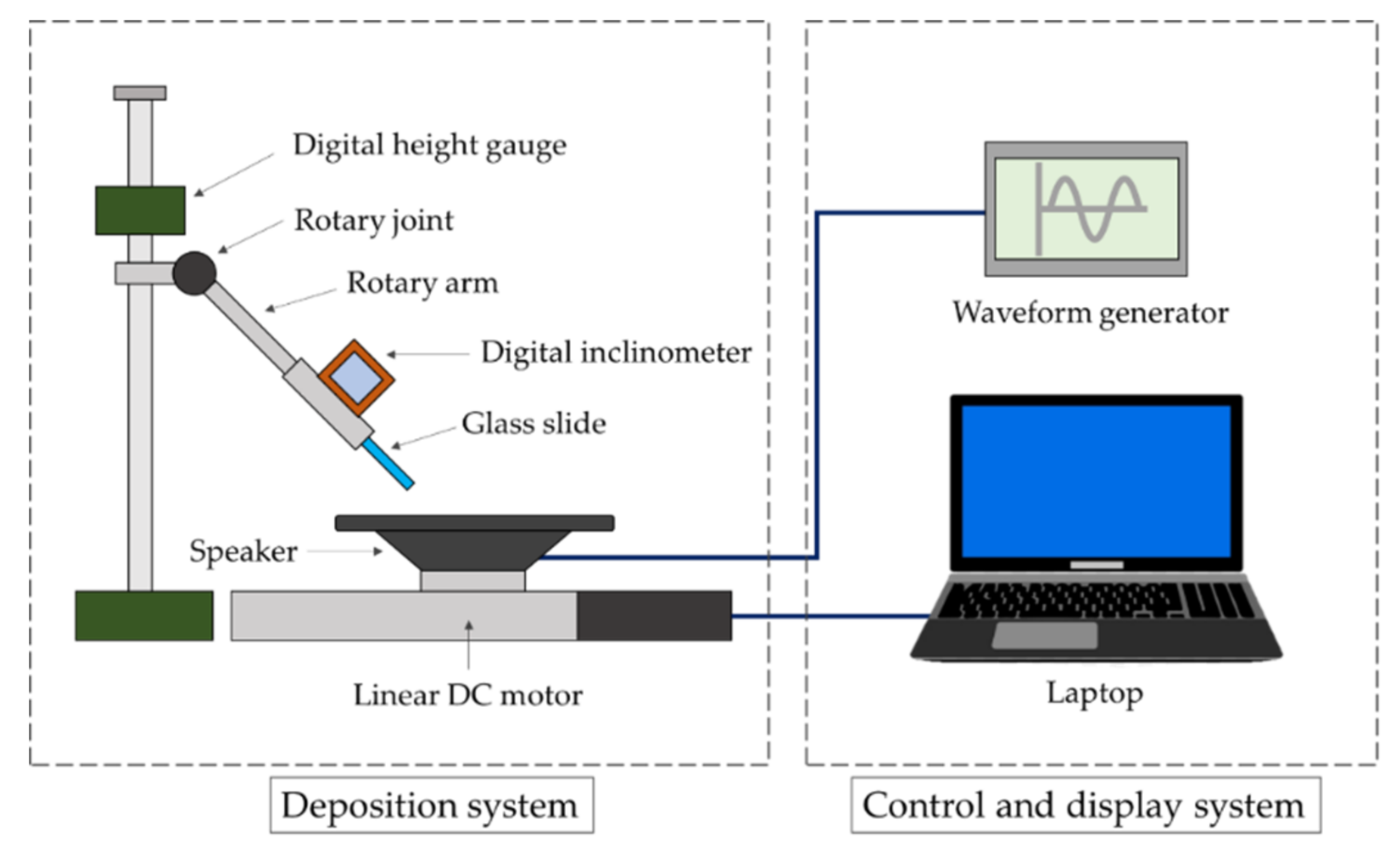
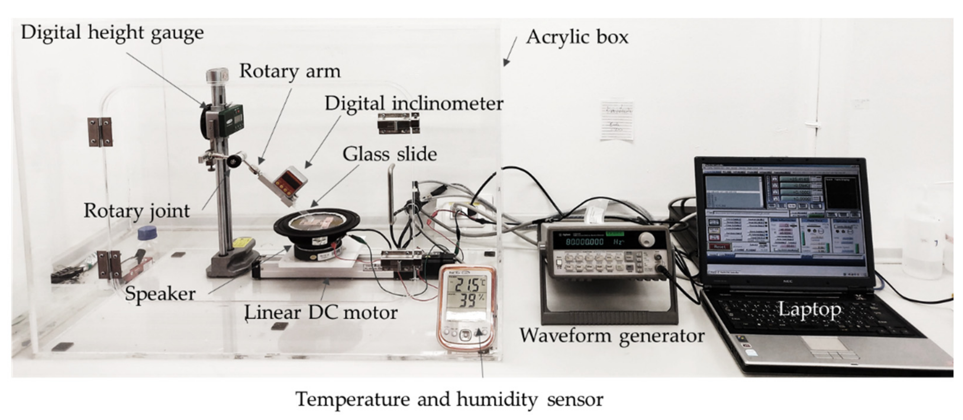
2.1. Development of the Vertical Vibration-Assisted Blade Coating Set

In this work, a vertical vibration-assisted blade coating set, named as VVBC, was developed for the first time to fabricate 2D periodic nanopatterned arrays, named VVBC, was developed for the first time to fabricate 2D periodic nanopatterned arrays. Figure 1 shows the schematic representing the experimental VVBC setup. A glass slide (76 mm × 26 mm × 1 mm, Marienfield) was used as a deposition blade and mounted on a rotary arm. The blade angle (θ) was controlled by a rotary joint and measured by a digital inclinometer. A low-cost speaker was used as a stage and a vibration transducer simultaneously. The translation of stage in a horizontal plane was controlled by a linear DC motor (Cool-Muscle, RL-45T-06-0200-N). The distance between blade and stage was able to be adjusted by using a digital height gauge (InSize, IN-1151-900).
In the deposition process, the linear motor was connected to a laptop for precisely controlling deposition speed, in the range of 1 μm/s to 0.3 cm/s, using Mach3Mill software. The speaker was connected to an arbitrary waveform generator (Agilent, Santa Clara, CA, USA, 33210A) for applying the vertical vibration frequency and amplitude in the range of 40 Hz–15 MHz and 50 mVP-P–10 VP-P, respectively. The deposition system was placed in an acrylic box for humidity control. The VVBC was assembled as shown in Figure 2.

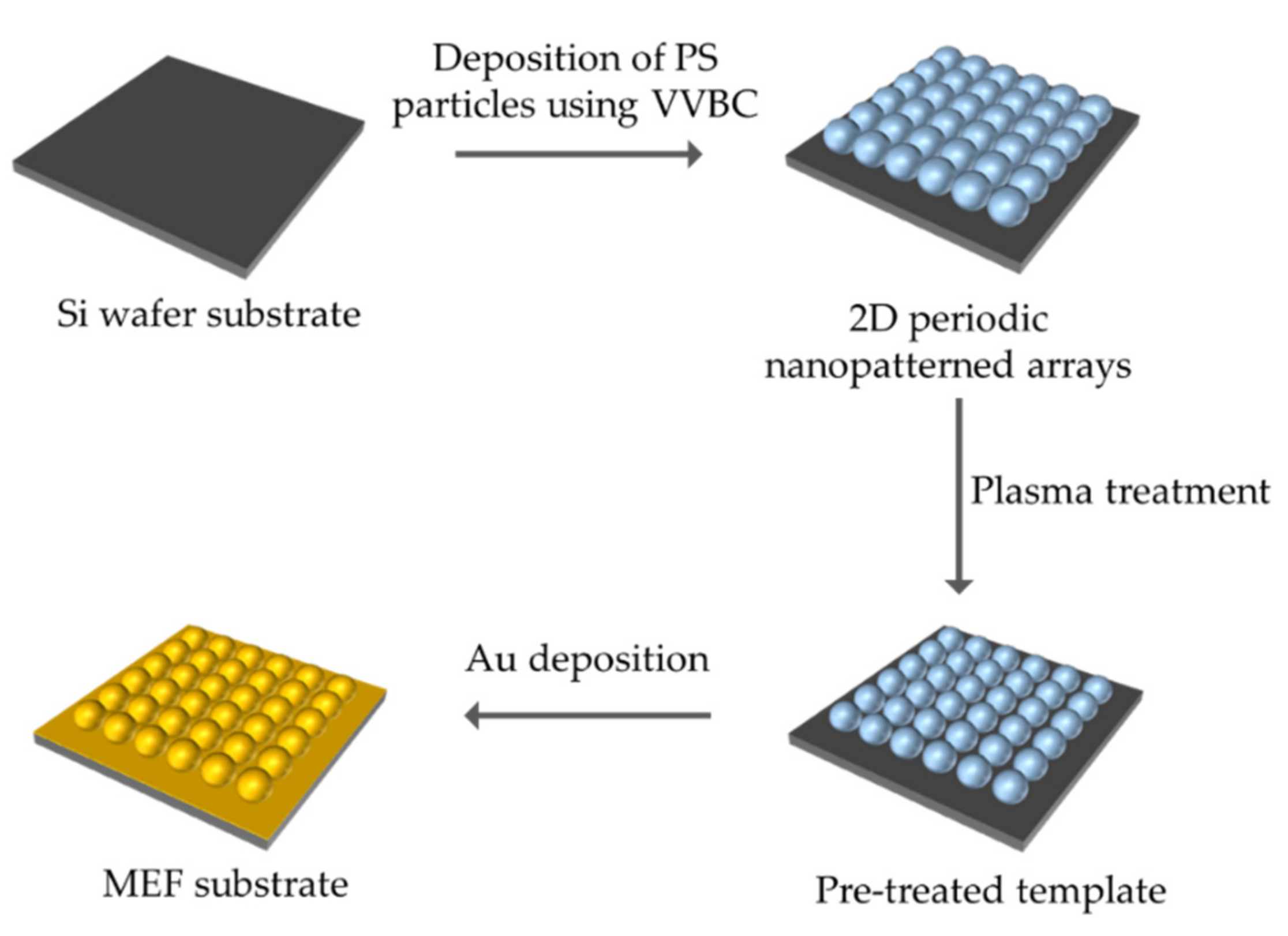
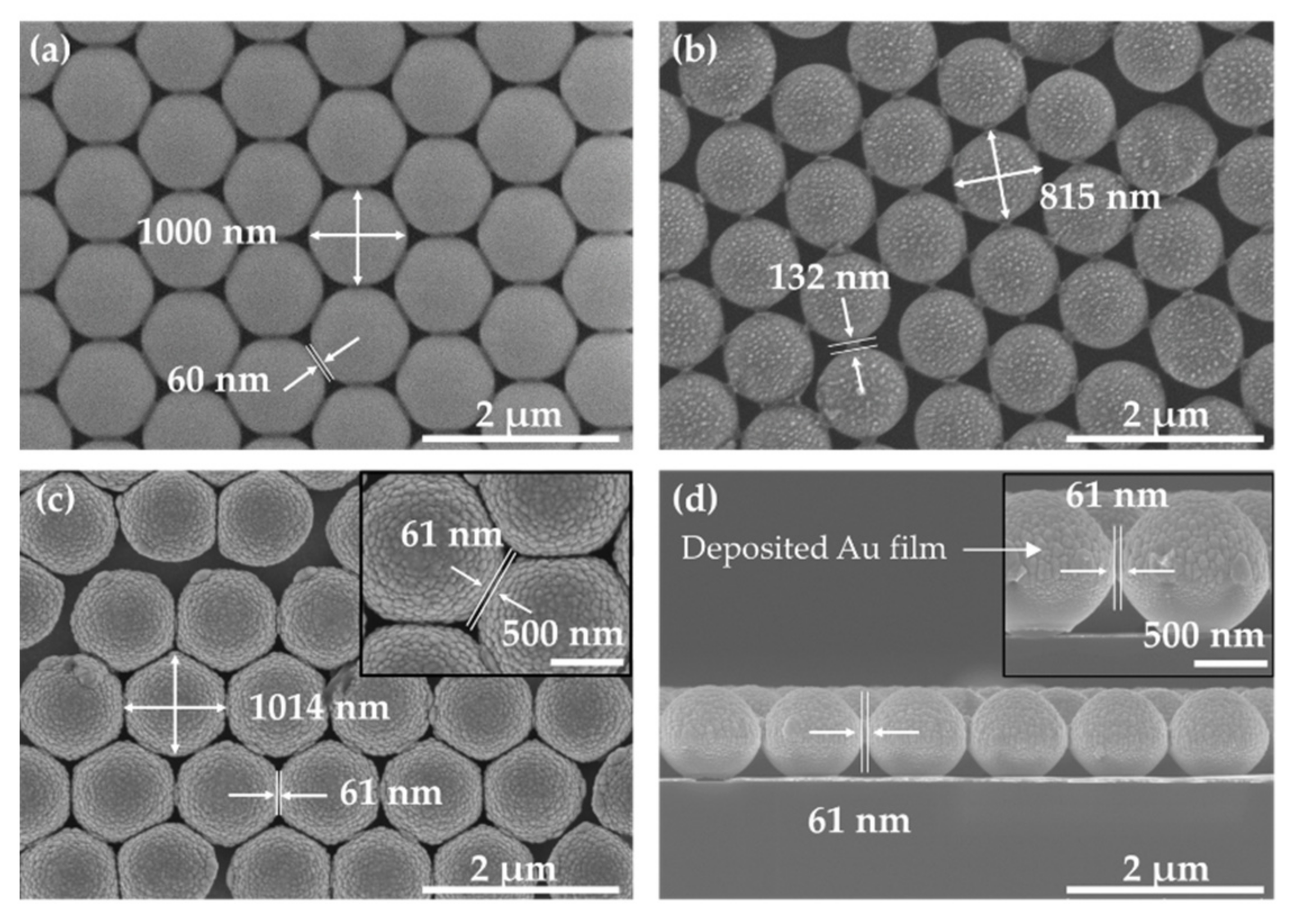
2.2. Fabrication of 2D Periodic Nanopatterned Arrays

A silicon wafer was cut into a small piece of 2 cm × 2 cm to be used as a substrate. After that, it was cleaned with deionized (DI) water and acetone under sonication and dried under a gentle stream of nitrogen gas. After the drying process, the substrate surface was modified by a plasma treatment under an oxygen atmosphere to improve its wettability. The well-treated substrate was placed on the stage at the center of a speaker, and the height between the blade end and the substrate surface was set to 0.1 mm.
To fabricate 2D periodic nanopatterned arrays, the polystyrene (PS) particles (obtained from Duke Scientific Corporation, Fremont, CA, USA), with an average particle diameter of 1.02 ± 0.02 μm in aqueous suspension (1% w/v), were collected in a total volume of 10 μL and injected into the gap between the deposition blade and the substrate. Then, the substrate was moved horizontally by a linear motor to a distance of 2 cm. The arrangement of PS colloid spheres deposited on the substrate under different deposition speeds (1–9 µm/s), deposition angles (30°–60°), vibration frequencies (50–90 Hz), and vibration amplitudes (50–150 mVP-P), were investigated. The experiments were carried out at the room temperature of 25 ± 1 °C, with a relative humidity of 55 ± 1% RH. For each deposition condition, the experiment was repeated 5 times. The optimized condition to accomplish the highest percentages of deposited area, monolayer structure, and HCP density of self-assembled periodic PS arrays, was revealed and further used to develop the MEF substrate.

2.3. Characterization of 2D Periodic Nanopatterned Arrays

The as-prepared PS films were photographed using a digital camera. Then, the captured images were analyzed using the image processing ImageJ software and MATLAB to investigate the percentages of the PS-deposited area and monolayer formation. A field-emission scanning electron microscope (FE-SEM) [Hitachi, Chiyoda City, Japan, SU8030] was used to observe the microscopic structure of the as-prepared films, and the percentage of HCP density was evaluated using a numerical method.

2.4. Preparation of MEF Substrate

To prepare the MEF substrate, the 2D periodic nanopatterned arrays prepared under the optimum condition obtained from previous sections were used as a template for Au deposition. Firstly, the template was exposed for 5 min of plasma treatment at an operating power of 30 W and a pressure of 0.2 Torr for adjusting the gap between particles to prevent a bulk film formation during the Au deposition process [24,25]. After that, the pre-treated template was coated with a Au thin film using magnetron sputtering. The sputtering system was evacuated to 5 mTorr, then filled with Ar gas before initiating the sputtering process at an operating power of 100 W for 10 min. The as-prepared MEF substrate was cut into pieces sized at 5 mm × 5 mm. The morphology of the Au films deposited onto the template was observed using FE-SEM. Figure 3 illustrates a schematic of the procedure used for fabricating the MEF substrate.

2.5. Investigating the Efficiency of MEF Substrate on Fluorescence Signal Enhacement

R6G, which is the standard dye for fluorescence measurement [26], was used to investigate the efficiency of as-prepared MEF substrates for enhancement of fluorescence signal. The different concentrations of R6G, from 10−3 to 10−10 M, were prepared by dissolving R6G powder (Sigma-Aldrich, St. Louis, MO, USA) with DI water. Then, 10 μL of the R6G solution was pipetted on the MEF substrate and covered with a glass cover slide.
The fluorescence spectrum of R6G was analyzed using a photoluminescence spectrophotometer (Photon Technology International, Kyoto, Japan, QM40). The excitation wavelength was selected at 532 nm, and the emission spectrum was recorded at 500–650 nm [26]. The average fluorescence intensities reported in this work were obtained from 5 measurements. The fluorescence enhancement factor (EF) of the MEF substrate was calculated using Equation (1) [27],
EF = I MEF I MEF blank I si I Si blank
where IMEF is the average fluorescence intensity of R6G at the maximum emission peak (λmax) on the MEF substrate, ISi is the average fluorescence intensity of R6G at λmax on the silicon substrate, IMEF(blank) is the average background fluorescence intensity of the MEF substrate, and ISi(blank) is the average background fluorescence intensity of the silicon substrate.
In addition, the sensitivity of the MEF substrate on R6G measurement was further studied by calculating the limit of detection (LOD), Tokyo, Japan the minimum concentration of the analyte that can be distinguished, and the limit of quantitation (LOQ), Tokyo, Japan, which is the minimum concentration that can be reliably measured. By recording the background fluorescence signal (noise) of the silicon and MEF substrates, the LOD and LOQ can be calculated as 3 σ/S and 10 σ/S, respectively, where σ is the standard deviation and S is the slope of the calibration curve [31].

3. Results and Discussions

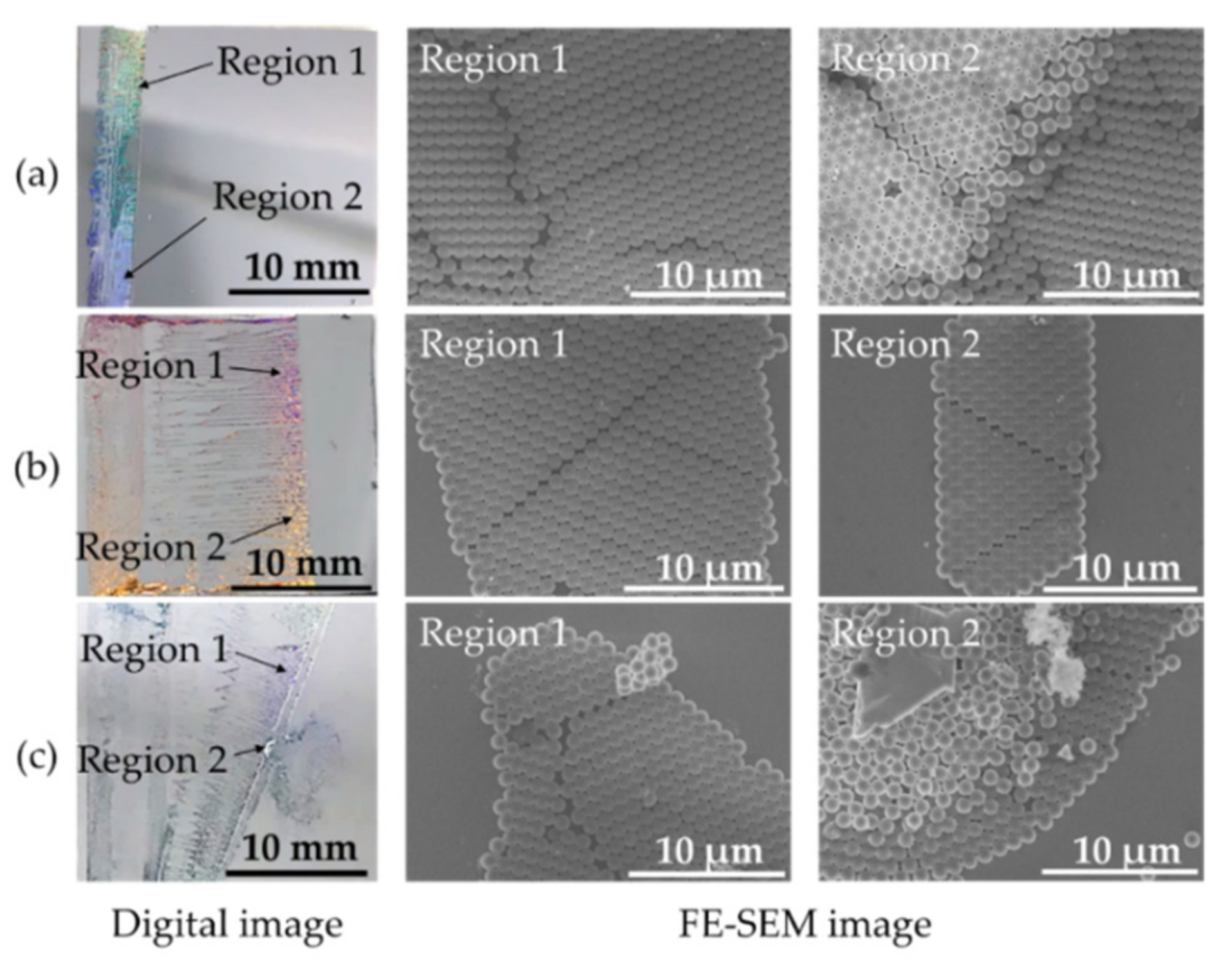
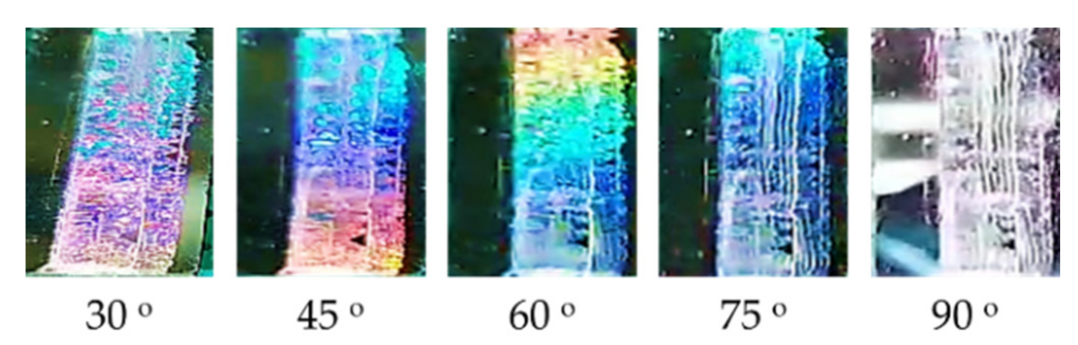
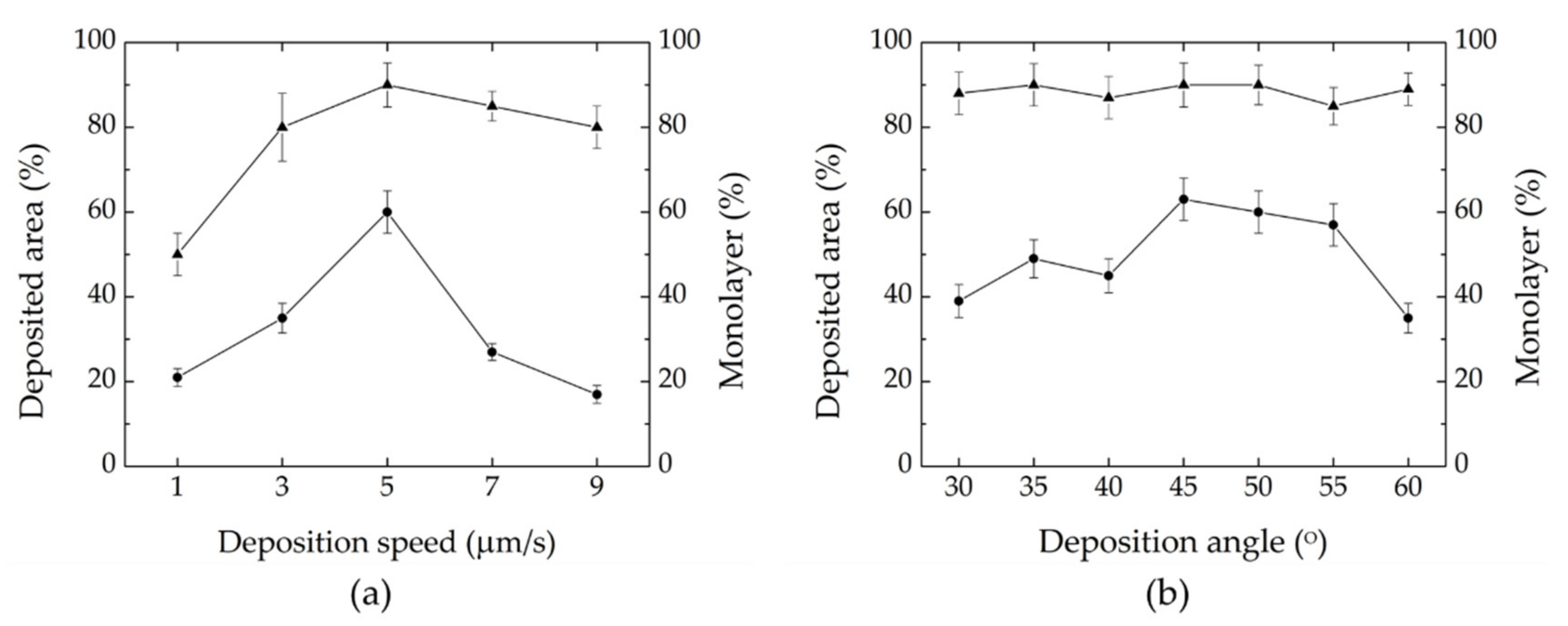
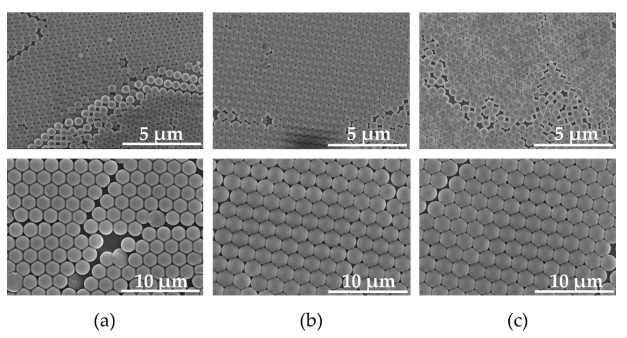
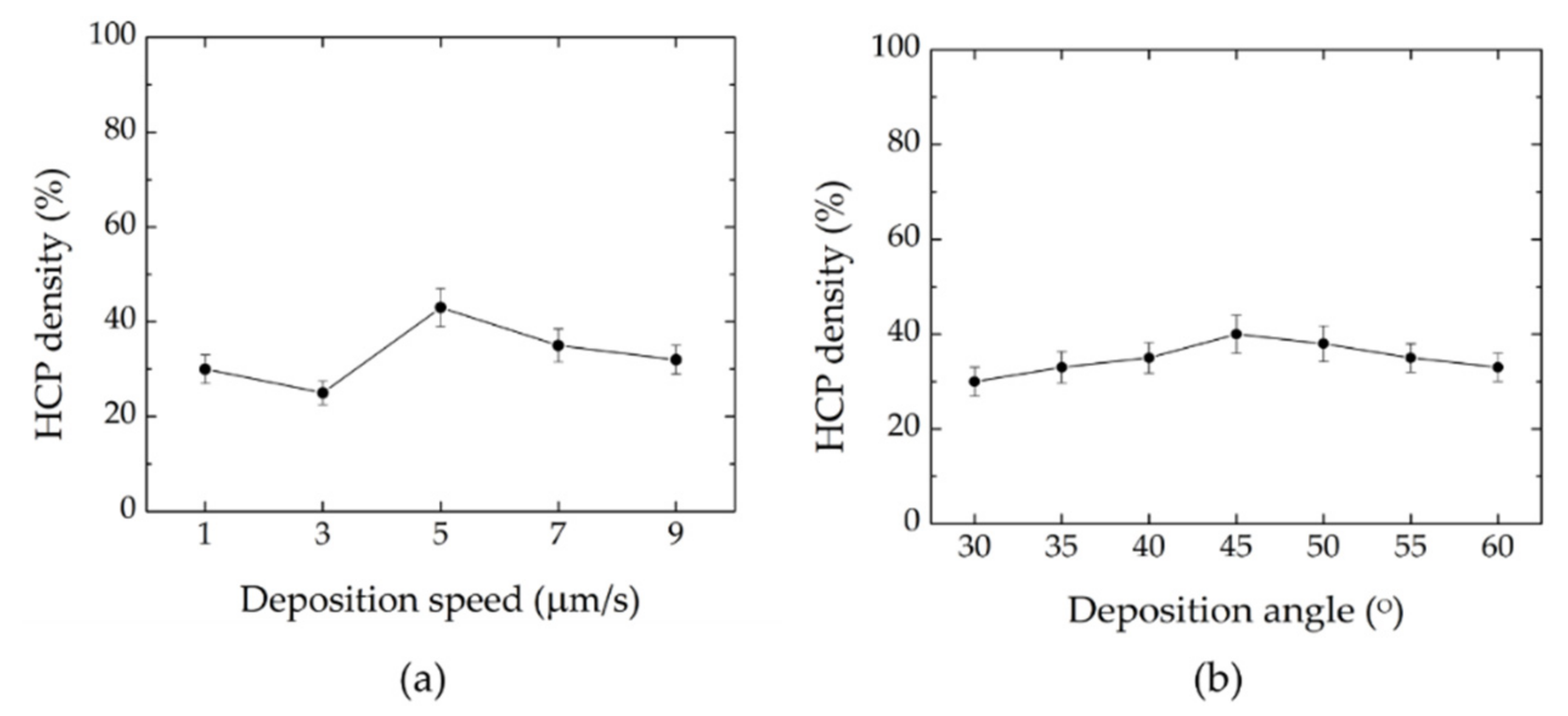
3.1. Effects of Deposition Speed and Deposition Angle on Self-Assembly of PS Colloidal Particles

Firstly, the deposition speed and angle affecting the self-assembly of PS particles on a silicon wafer substrate using a VVBC without vibration were investigated. The deposition angle was set at 45° and the deposition speeds were adjusted to be 1, 3, 5, 7, and 9 µm/s, respectively. The film quality of the as-prepared PS microsphere arrays deposited on a substrate was inspected using a digital camera and an FE-SEM. Figure 4 shows the captured digital images and FE-SEM images of the self-assembled PS films.
As seen in the digital images of Figure 4, the interference patterns in region 1 could be viewed directly with the naked eye, indicating the existence of PS particles on the substrate. This phenomenon was a result of the self-assembly arrangement of the PS spheres in HCP monolayer arrays acting as a waveguide in the photonic crystal structure [29,32]. A colorful interference pattern was observed when the angle of incident light was changed, as shown in Figure 5. Similarly, the FE-SEM images in Figure 4 confirmed the presence of a self-assembled monolayer of PS spheres. However, the multilayer arrays formation was also found in region 2, leading to no interference pattern appearance due to Bragg’s law [29,33].
Using an image processing technique to evaluate the percentages of deposited area and monolayer, it was found that the highest percentage of deposited area and monolayer were attained by setting the deposition angle and deposition speed at 45° and 5 µm/s, respectively, without vibration assistance, as shown in Figure 6a. However, when the deposition speed was less than 5 µm/s, the monolayer formation decreased because the evaporation rate of the solvent was higher than the film formation rate. Furthermore, the monolayer formation also decreased when the deposition speed was increased to above 5 µm/s, as a result of the slowing film formation rate [31]. This indicated that the deposition speed of 5 µm/s was close to the evaporation rate of the solvent [29,34,35].
By considering the FE-SEM images in Figure 7, it was found that a non-uniform HCP structure was mostly formed at the deposition speed of below 5 µm/s due to the formation of multilayers. On the other hand, the uniform HCP structure with several line defects occurring at the grain boundary was formed at the deposition speed of above 5 µm/s. This was a result of a non-continuous film structure forming at a deposition speed higher than the evaporation rate of the solvent [30,35]. The defect-free HCP structure was obtained under the fixed deposition speed of 5 µm/s. Figure 8a shows the HCP density percentage, which was calculated using a numerical method. From all results, it could be concluded that the deposition speed of 5 µm/s was the optimum value to prepare the PS monolayer with the HCP structure.
After finishing the deposition speed optimization, the effect of the deposition angle on as-prepared PS films quality was considered as well. The deposition process was carried out using the VVBC at a deposition speed of 5 µm/s and the deposition angles in a range of 30°–60° without vibration assistance. Figure 6b shows the effect of deposition angle on the percentages of the deposited area and monolayer of the self-assembled PS films. It indicated that the interaction between a colloidal droplet and a substrate at the deposition angles of 30°–50° was good, resulting in the formation of a large deposited area [33,35]. Especially at the deposition angle of 45°, the largest deposited area was achieved due to it occurring the greatest number of interactions. On the other hand, it was found that the deposited area significantly reduced when the deposition angle was increased to above 55° because the content of the PS colloidal particle residues on the back side of the deposition blade was low [34]. Figure 8b shows the HCP density percentage, which was calculated using a numerical method. From all optimizations, it was evident that the optimum condition for preparing a low-defect PS sphere monolayer film was the deposition speed of 5 µm/s and the deposition angle of 45°. However, the film quality could be improved by applying external energy to a PS particle during the coating process. With the appropriate energy, the particles attempt to reduce their surface energy by arranging into a close-packed structure [36,37]. In this work, a vertical vibration was therefore used as a method for applying energy to particles. The appropriate values of vibration frequency and vibration amplitude were determined with certainty.

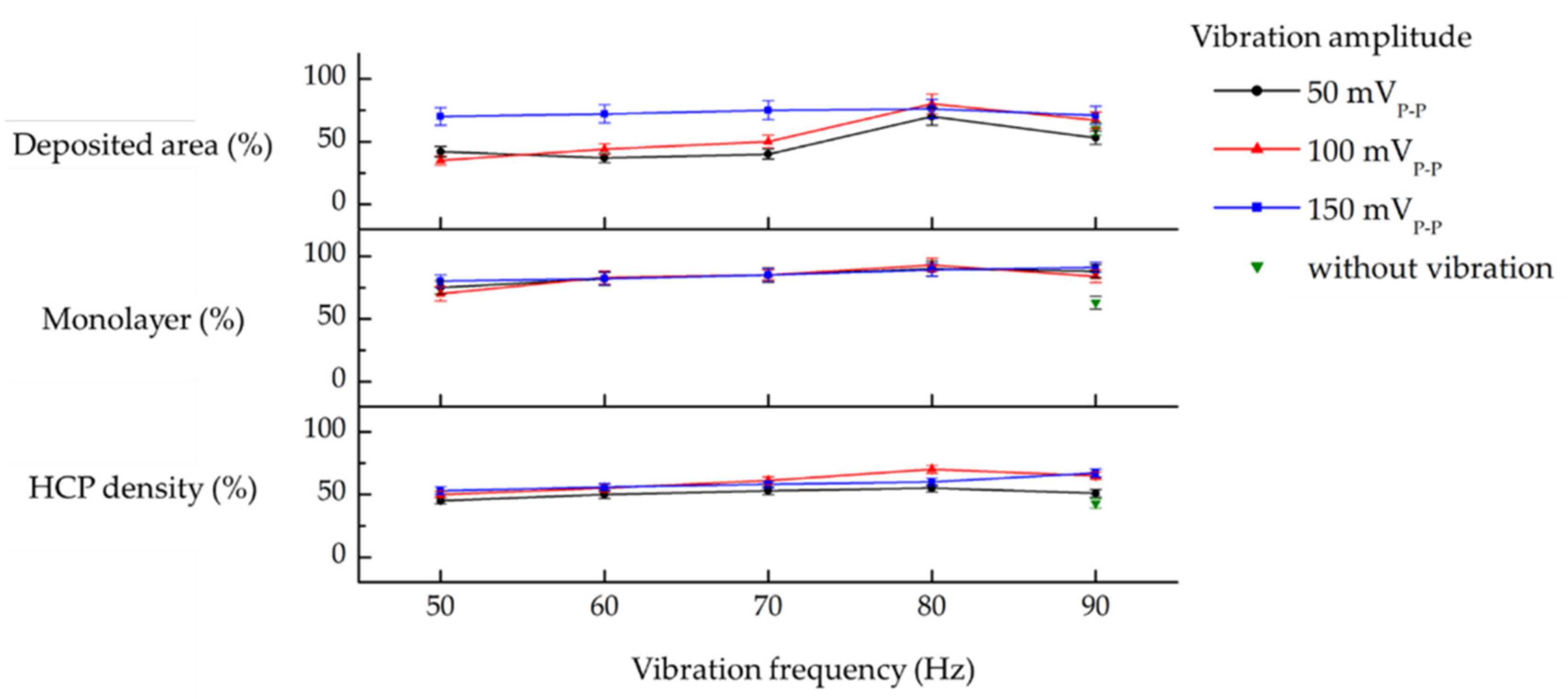
3.2. Effects of Vibration Frequency and Vibration Amplitude on Self-Assembly of PS Colloidal Particles

To determine the effect of applying vertical vibration during a coating process, the process was conducted under the following conditions: the deposition angle was 45°, the deposition speed was 5 µm/s, the vibration frequencies were varied in a range of 50–90 Hz, and the vibration amplitudes were 50 and 100 mVP-P. Figure 9 shows the obtained result; it was found that applying vertical vibration to a coating process obviously affected the film quality, especially the HCP and monolayer formation occurring in the presence of meniscus stability [38]. At a frequency of 80 Hz and an amplitude of 100 mVP-P, the film quality was dramatically improved because this frequency might be close to the natural frequency of PS colloidal particles with a diameter of 1 μm, resulting in particle vibration at its highest energy. With the increasing vibration energy, the evaporation rate of the suspension increased due to the heat generated from the oscillation, leading to the increase in deposited area and the decrease in interfacial tension between PS particles [28]. The results showed that the colloidal particles of the 2D hexagonal array was successfully prepared by the combination of a convective deposition with substrate vibration in a vertical direction.

3.3. Fluorescence Enhancement Efficiency of the Developed MEF Substrate

Figure 10a,b clearly show that the morphology of the 2D periodic nanopatterned template could be modified using a plasma treatment. By depositing Au thin film on the modified template, the MEF structure exhibited the larger particle size, increasing the surface roughness, as seen in Figure 10c. In Figure 10d, the inter-particle distance was approximately 61 ± 1.8 nm, corresponding with the desirable distance [3,11].
Figure 11 shows the fluorescence spectra of R6G with an emission peak at 556 nm on the silicon and MEF substrates. Using the silicon substrate, the fluorescence spectra of R6G were unable to observe at a concentration of below 1 × 10⁻⁶ M, as shown in Table 1. On the contrary, with the presence of the MEF substrate, the fluorescence spectra of R6G were able to record down to 1 × 10⁻⁸ M due to the MEF effect. The developed MEF substrate showed a good performance for R6G fluorescence enhancement due to the gap size of 61 ± 1.8 nm, as shown in Figure 10d, corresponding to the required feature size for the MEF phenomenon. This hotspot acted as an amplifier for the surrounding R6G molecules, resulting in a higher fluorescence intensity. Moreover, the surface roughness of metals deposited on the MEF substrate also played an important role in providing more LSPR fields, causing the increase in fluorescence intensity [39]. However, at a high concentration of R6G, the enhancement factor reduced due to the concentration quenching effect [40]. To estimate the fluorescence enhancement efficiency of the MEF substrate, the LOD and LOQ were determined. The calculated LOD and LOQ were found to be 3.3 × 10⁻⁹ M and 1.01 × 10⁻⁸ M, respectively.

4. Conclusions

A novel method for preparing a large-area monolayer of 2D periodic nanopatterned arrays using the vertical vibration-assisted convective deposition technique has been successfully proven in this work. It was an alternative method for preparing 2D periodic nanopatterned arrays with relatively low costs and simplicity compared to those reported in previous works [27,28,41,42]. The developed MEF substrate showed high performance in the fluorescence signal enhancement of R6G. The results suggest that the developed MEF substrate is a potential tool for R6G label-based fluorescent detection. Furthermore, the developed MEF can be utilized for fluorescence enhancement of other fluorescent dyes with the excitation and emission wavelengths in a range of 500–650 nm, such as Cyanine-3 (Cy3), Maleimide, Tetramethylrhodamine (TRITC), DyLightTM 550, and so on. However, according to LSPR phenomenon’s dependence on the metal nanostructure, the fluorescence enhancement efficiency of the developed MEF can be further improved by decreasing the gap between particles [43] through decreasing the plasma treatment time on a nanopatterned PS template or increasing the Au thin film deposition time. For the applications on fluorescence-based biosensor platforms using this developed MEF substrate, it is being studied by our research group, and the results are expected to be presented soon.

Author Contributions

Conceptualization, K.D., K.T., M.H., A.K. and A.P.; methodology, K.D.; software, K.D.; validation, K.D.; resources, M.H. and A.K.; data curation, K.D.; writing—original draft preparation, K.T.; writing—review and editing, K.D.; supervision, M.H., A.K. and P.L. All authors have read and agreed to the published version of the manuscript.

Funding

This research was funded by the Petchra Pra Jom Klao Master’s Degree Scholarship from King Mongkut’s University of Technology Thonburi (KMUTT), Thailand (Grant no. 40/2561). The authors also acknowledge the National Electronic and Computer Technology Center (Grant no. P1952720, P2050221).

Institutional Review Board Statement

Not applicable.

Informed Consent Statement

Not applicable.

Acknowledgments

K.D. gratefully acknowledges the financial support provided by the Petchra Pra Jom Klao Master’s Degree Scholarship from King Mongkut’s University of Technology Thonburi (KMUTT), Thailand (Grant no. 40/2561).

Conflicts of Interest

The authors declare no conflict of interest.

References

  1. Alder, N.N. Fluorescence Spectroscopy and Its Applications in Analysing Biomolecular Processes. Biomol. Bioanal. Tech. Methodol. Appl. 2019, 333–363. [Google Scholar] [CrossRef]
  2. Jeong, Y.; Kook, Y.-M.; Lee, K.; Koh, W.-G. Metal enhanced fluorescence (MEF) for biosensors: General approaches and a review of recent developments. Biosens. Bioelectron. 2018, 111, 102–116. [Google Scholar] [CrossRef] [PubMed]
  3. Zhang, Y.; Aslan, K.; Previte, M.J.R.; Geddes, C.D. Metal-Enhanced Excimer (P-type) Fluorescence. Chem. Phys. Lett. 2008, 458, 147–151. [Google Scholar] [CrossRef] [PubMed] [Green Version]
  4. Dragan, A.; Geddes, C. Metal-enhanced fluorescence: The role of quantum yield, Q0, in enhanced fluorescence. Appl. Phys. Lett. 2012, 100, 093115. [Google Scholar] [CrossRef] [Green Version]
  5. Badshah, M.A.; Koh, N.Y.; Zia, A.W.; Abbas, N.; Zahra, Z.; Saleem, M.W. Recent Developments in Plasmonic Nanostructures for Metal Enhanced Fluorescence-Based Biosensing. Nanomaterials 2020, 10, 1749. [Google Scholar] [CrossRef]
  6. Sugawa, K.; Tamura, T.; Tahara, H.; Yamaguchi, D.; Akiyama, T.; Otsuki, J.; Kusaka, Y.; Fukuda, N.; Ushijima, H. Metal-Enhanced Fluorescence Platforms Based on Plasmonic Ordered Copper Arrays: Wavelength Dependence of Quenching and Enhancement Effects. ACS Nano 2013, 7, 9997–10010. [Google Scholar] [CrossRef]
  7. Darvill, D.; Centeno, A.; Xie, F. Plasmonic fluorescence enhancement by metal nanostructures: Shaping the future of bionanotechnology. Phys. Chem. Chem. Phys. 2013, 15, 15709–15726. [Google Scholar] [CrossRef] [PubMed]
  8. Mei, Z.; Tang, L. Surface-Plasmon-Coupled Fluorescence Enhancement Based on Ordered Gold Nanorod Array Biochip for Ultrasensitive DNA Analysis. Anal. Chem. 2017, 89, 633–639. [Google Scholar] [CrossRef]
  9. Petryayeva, E.; Krull, U. Localized Surface Plasmon Resonance: Nanostructures, Bioassays and Biosensing—A Review. Anal. Chim. Acta 2011, 706, 8–24. [Google Scholar] [CrossRef]
  10. Hutter, E.; Fendler, J.H. Exploitation of Localized Surface Plasmon Resonance. Adv. Mater. 2004, 16, 1685–1706. [Google Scholar] [CrossRef]
  11. Rahaman, M.; Moras, S.; He, L.; Madeira, T.; Zahn, D. Fine Tuning of Localized Surface Plasmon Resonance of Metal Nanostructures from Near-Infrared to Blue prepared by Nanosphere Lithography. J. Appl. Phys. 2020, 128, 233104. [Google Scholar] [CrossRef]
  12. Sui, N.; Wang, L.; Yan, T.; Liu, F.; Sui, J.; Jiang, Y.; Wan, J.; Liu, M.; Yu, W.W. Selective and sensitive biosensors based on metal-enhanced fluorescence. Sens. Actuators B Chem. 2014, 202, 1148–1153. [Google Scholar] [CrossRef]
  13. Jung, J.-Y.; Yang, W.-G.; Hong, S.-h.; Kim, G.-H.; Hwang, K.; Chae, W.-S. Amplified fluorescence imaging using photonic Ag nanotip array: A comparative study on surface morphology effects. Appl. Surf. Sci. 2020, 529, 147139. [Google Scholar] [CrossRef]
  14. Pale, V.; Kauppinen, C.; Selin, J.; Sopanen, M.; Tittonen, I. Fluorescence-enhancing plasmonic silver nanostructures using azopolymer lithography. RSC Adv. 2016, 6, 48129–48136. [Google Scholar] [CrossRef]
  15. Cinel, N.A.; Cakmakyapan, S.; Butun, S.; Ertas, G.; Ozbay, E. E-Beam lithography designed substrates for surface enhanced Raman spectroscopy. Photonics Nanostruct. Fundam. Appl. 2015, 15, 109–115. [Google Scholar] [CrossRef] [Green Version]
  16. Aiempanakit, M.; Jearnkulprasert, N.; Panyajirawut, P. Patterning of Nanoparticle Arrays by Self-assembly Lithography. Mater. Today Proc. 2017, 4, 6009–6014. [Google Scholar] [CrossRef]
  17. Kasani, S.; Curtin, K.; Wu, N. A review of 2D and 3D plasmonic nanostructure array patterns: Fabrication, light management and sensing applications. Nanophotonics 2019, 8, 2065–2089. [Google Scholar] [CrossRef]
  18. Zhao, X.; Wen, J.; Li, L.; Wang, Y.; Wang, D.; Chen, L.; Zhang, Y.; Du, Y. Architecture design and applications of nanopatterned arrays based on colloidal lithography. J. Appl. Phys. 2019, 126, 141101. [Google Scholar] [CrossRef]
  19. Sitpathom, N.; Dawes, J.M.; Osotchan, T.; Kumnorkaew, P.; Suwanna, S.; Sinsarp, A.; Muangnapoh, T. Tuning higher order electric field resonances in plasmonic hexagonal arrays by oxygen-plasma treatment. Appl. Phys. B 2021, 127, 71. [Google Scholar] [CrossRef]
  20. Born, P.; Munoz, A.; Cavelius, C.; Kraus, T. Crystallization Mechanisms in Convective Particle Assembly. Langmuir. 2012, 28, 8300–8308. [Google Scholar] [CrossRef]
  21. Dimitrov, A.S.; Nagayama, K. Continuous Convective Assembling of Fine Particles into Two-Dimensional Arrays on Solid Surfaces. Langmuir 1996, 12, 1303–1311. [Google Scholar] [CrossRef]
  22. Zhang, C.; Cvetanovic, S.; Pearce, J.M. Fabricating ordered 2-D nano-structured arrays using nanosphere lithography. MethodsX 2017, 4, 229–242. [Google Scholar] [CrossRef]
  23. Wang, X.; Shi, F.; Gao, X.; Fan, C.; Huang, W.; Feng, X. A sol–gel dip/spin coating method to prepare titanium oxide films. Thin Solid Film. 2013, 548, 34–39. [Google Scholar] [CrossRef]
  24. Jibowu, T. Nano-spherical lithography for nanopatterning. Front. Nanosci. Nanotechnol. 2016, 2, 1–5. [Google Scholar] [CrossRef] [Green Version]
  25. Joshi, K.; Muangnapoh, T.; Stever, M.D.; Gilchrist, J.F. Effect of Ionic Strength and Surface Charge on Convective Deposition. Langmuir 2015, 31, 12348–12353. [Google Scholar] [CrossRef]
  26. Canalejas-Tejero, V.; Ibisate, M.; Golmayo, D.; Blanco, A.; López, C. Qualitative and Quantitative Analysis of Crystallographic Defects Present in 2D Colloidal Sphere Arrays. Langmuir 2012, 28, 161–167. [Google Scholar] [CrossRef] [PubMed] [Green Version]
  27. Muangnapoh, T.; Weldon, A.L.; Gilchrist, J. Enhanced colloidal monolayer assembly via vibration-assisted convective deposition. Appl. Phys. Lett. 2013, 103, 181603. [Google Scholar] [CrossRef] [Green Version]
  28. Das, S.; Duraia, E.-s.M.; Velev, O.D.; Gatabi, J.R.; Beall, G.W. Reduction of defects in self-assembling colloidal monolayer via surface modifiers and periodic mechanical vibration. Surf. Coat. Technol. 2017, 319, 353–358. [Google Scholar] [CrossRef]
  29. Joshi, K.; Gilchrist, J.F. Effect of added surfactant on convective assembly of monosized microspheres. Appl. Phys. Lett. 2020, 116, 083702. [Google Scholar] [CrossRef]
  30. Yuan, Z.; Burckel, D.B.; Atanassov, P.; Fan, H. Convective self-assembly to deposit supported ultra-thin mesoporous silica films. J. Mater. Chem. 2006, 16, 4637–4641. [Google Scholar] [CrossRef]
  31. Pang, Y.; Rong, Z.; Xiao, R.; Wang, S. “Turn on” and label-free core−shell Ag@SiO2 nanoparticles-based metal-enhanced fluorescent (MEF) aptasensor for Hg2+. Sci. Rep. 2015, 5, 9451. [Google Scholar] [CrossRef] [Green Version]
  32. Ye, B.; Rong, F.; Gu, H.; Xie, Z.; Cheng, Y.; Zhao, Y.; Gu, Z. Bioinspired angle-independent photonic crystal colorimetric sensing. Chem. Commun. 2013, 49, 5331–5333. [Google Scholar] [CrossRef] [PubMed] [Green Version]
  33. Prevo, B.G.; Velev, O.D. Controlled, Rapid Deposition of Structured Coatings from Micro- and Nanoparticle Suspensions. Langmuir 2004, 20, 2099–2107. [Google Scholar] [CrossRef] [PubMed]
  34. Kumnorkaew, P.; Ee, Y.-K.; Tansu, N.; Gilchrist, J.F. Investigation of the Deposition of Microsphere Monolayers for Fabrication of Microlens Arrays. Langmuir 2008, 24, 12150–12157. [Google Scholar] [CrossRef] [PubMed]
  35. Born, P.; Blum, S.; Munoz, A.; Kraus, T. Role of the Meniscus Shape in Large-Area Convective Particle Assembly. Langmuir 2011, 27, 8621–8633. [Google Scholar] [CrossRef]
  36. Mahynski, N.A.; Panagiotopoulos, A.Z.; Meng, D.; Kumar, S.K. Stabilizing colloidal crystals by leveraging void distributions. Nat. Commun. 2014, 5, 4472. [Google Scholar] [CrossRef] [Green Version]
  37. Edison, J.R.; Dasgupta, T.; Dijkstra, M. Stabilizing the hexagonal close packed structure of hard spheres with polymers: Phase diagram, structure, and dynamics. J. Chem. Phys. 2016, 145, 054902. [Google Scholar] [CrossRef] [Green Version]
  38. Seiwert, J.; Pierre, J.; Dollet, B. Coupled vibrations of a meniscus and liquid films. J. Fluid Mech. 2015, 788, 183–208. [Google Scholar] [CrossRef] [Green Version]
  39. Byun, K.M.; Yoon, S.J.; Kim, D. Effect of surface roughness on the extinction-based localized surface plasmon resonance biosensors. Appl. Opt. 2008, 47, 5886–5892. [Google Scholar] [CrossRef]
  40. Robeson, J.L.; Tilton, R.D. Effect of concentration quenching on fluorescence recovery after photobleaching measurements. Biophys. J. 1995, 68, 2145–2155. [Google Scholar] [CrossRef] [Green Version]
  41. Hassan, H.K.; Stepanyants, Y.A. Resonance properties of forced oscillations of particles and gaseous bubbles in a viscous fluid at small Reynolds numbers. Phys. Fluids 2017, 29, 101703. [Google Scholar] [CrossRef]
  42. Sitpathom, N.; Kumnorkaew, P.; Muangnapoh, T.; Osotchan, T. Optical diffraction of binary-nanoparticle film prepared by convective deposition with vibration assistance. Mater. Today Proc. 2018, 5, 11101–11105. [Google Scholar] [CrossRef]
  43. Feng, A.L.; You, M.L.; Tian, L.; Singamaneni, S.; Liu, M.; Duan, Z.; Lu, T.J.; Xu, F.; Lin, M. Distance-Dependent Plasmon-Enhanced Fluorescence of Upconversion Nanoparticles using Polyelectrolyte Multilayers as Tunable Spacers. Sci. Rep. 2015, 5, 7779. [Google Scholar] [CrossRef] [PubMed]
Figure 1. Schematic representation of the whole setup of the VVBC.
Processes 10 00202 g001
Figure 2. Digital images of the assembled VVBC.
Processes 10 00202 g002
Figure 3. Schematic illustration of the MEF substrate preparation.
Processes 10 00202 g003
Figure 4. Digital images and FE-SEM images of the as-prepared PS films at two regions. Grown with different deposition speeds: (a) 1, (b) 5, and (c) 9 µm/s.
Processes 10 00202 g004
Figure 5. Digital images of the as-prepared PS films deposited on a substrate taken from different angles.
Processes 10 00202 g005
Figure 6. Calculated percentages of deposited area (●) and monolayer (▲) of self-assembled PS films with: (a) varying deposition speed and (b) varying deposition angle.
Processes 10 00202 g006
Figure 7. FE-SEM images of the self-assembled PS films prepared on a substrate with the deposition angle of 45° and the different deposition speeds: (a) 1, (b) 5, and (c) 9 µm/s.
Processes 10 00202 g007
Figure 8. HCP density percentage of self-assembled PS films with: (a) varying deposition speeds and (b) varying deposition angles.
Processes 10 00202 g008
Figure 9. Percentages of deposited area, monolayer, and HCP density of self-assembled PS films with vibration frequency and amplitude.
Processes 10 00202 g009
Figure 10. FE-SEM images of: (a) as-prepared 2D periodic nanopattern template, (b) modified template, and (c) and (d) MEF substrate.
Processes 10 00202 g010
Figure 11. Fluorescence spectra of R6G solution measured on: (a) silicon substrate and (b) MEF substrate.
Processes 10 00202 g011
Table 1. Fluorescence intensity of R6G measured on silicon substrate and MEF substrate.
R6G Concentration
(M)
Fluorescence Intensity (a.u.)Enhancement Factor
(Fold)
Silicon SubstrateMEF Substrate
1 × 10−3573.992973.945.19
5 × 10−4476.422750.895.77
1 × 10−4346.272445.677.06
5 × 10−5273.552274.488.31
1 × 10−5162.0541917.4113.62
5 × 10−695.0721672.8417.59
1 × 10−647.181411.9451.22
5 × 10⁻⁷N/A1228.38N/A
1 × 10⁻⁷N/A895.32N/A
5 × 10⁻⁸N/A666.29N/A
1 × 10⁻⁸N/A346.12N/A
Where N/A = not available.
Publisher’s Note: MDPI stays neutral with regard to jurisdictional claims in published maps and institutional affiliations.

