Article

Optical Properties of Tungsten: A Parametric Study to Characterize the Role of Roughness, Surface Composition and Temperature

by
Federica Pappalardo
1,*,
Francisco Romero Lairado
1,
Cyprien Louis de Canonville
1,2,
Céline Martin
1,
Gregory Giacometti
1,
Guillaume Serin
1,
Eric Salomon
1,
Thierry Angot
1,
Laurent Gallais
2,
Régis Bisson
1 and
Marco Minissale
1,*
1
Aix-Marseille Univ, CNRS, PIIM, UMR 7345, 13007 Marseille, France
2
Aix-Marseille Univ, CNRS, Centrale Marseille, Institut Fresnel, 13007 Marseille, France
*
Authors to whom correspondence should be addressed.
Optics 2022, 3(3), 216-224; https://doi.org/10.3390/opt3030021
Submission received: 20 June 2022 / Revised: 30 June 2022 / Accepted: 1 July 2022 / Published: 5 July 2022
(This article belongs to the Special Issue Laser–Matter Interaction)

Abstract

:
Tungsten (W) is the material selected for the divertor exhaust of the international nuclear fusion experiment ITER. In this harsh environment, the interactions of heat loads and ion fluxes with W can induce temporary or permanent evolution in the optical properties. Poor knowledge of such evolution during a plasma operation can lead to errors in temperature measurements performed by optical diagnostics. Therefore, it is of fundamental importance to characterize possible changes in W optical properties. In this work, we studied the role of morphology and temperature on the optical response of W. The reflectivities of five W samples with different roughness values (20–100 nm) were measured during laser annealing (25–800 °C) in the visible and near-infrared domains (500–1100 nm). We observed an increase in reflectivity after annealing and we demonstrated that it was due to a change in the chemical composition of the surface, in particular a reduction in the amount of native oxide. Moreover, we show that roughness does not sensibly vary in the investigated temperature range. By highlighting the role played by roughness and surface impurities (e.g., oxide), we provide insight in how W optical properties can evolve in tokamaks where high ion fluxes, heat loads, and impurities can induce the evolution of both the morphology and surface composition of W.

1. Introduction

Tungsten (W) is the material selected for the divertor exhaust of the international nuclear fusion experiment ITER and it is expected to withstand high heat loads (≈20 MW/m 2 in the stationary regime) and high ion fluxes (up to 10 24 m 2 s 1 ) of hydrogen isotopes (deuterium and tritium, the fusion fuel), helium, and other possible impurities (e.g., oxygen) [1]. The interactions of heat loads and ion fluxes with tungsten can induce temporary or permanent changes in its optical properties. Poor knowledge of the evolution of optical properties of the divertor during a plasma operation could lead to errors in temperature measurements performed by optical diagnostics. It is necessary to minimize such errors to prevent possible failure of thermography diagnostics and to ensure a proper operation of the reactor. Among the different diagnostics, we can cite infrared (IR) thermal cameras and pyrometers [2]. The response of such devices is directly linked to the emissivity of the targeted material in a specific wavelength range [3], which is strongly influenced by the surface state of the material (roughness, cracks, presence of oxide, and other contaminations) [4,5]. Previous studies have proved that the interaction of charged particles with tungsten can induce material modifications, from microscopic lattice defects to mesoscopic damages, such as surface blisters [6] and near-surface bubbles [7,8], which evolve upon thermal annealing and can be responsible for a modified fuel inventory in the reactor walls [9]. Therefore, the plasma–wall interaction can modify the roughness of the divertor, either decreasing it due to W erosion or increasing it due to deposition. In particular, the deposition can create layers where different elements (W, C, O, …) are mixed [10], and it has been recently demonstrated that emissivity strongly varies depending on the deposition areas, due to the physical–chemical properties of the deposit [11]. The presence of such (near)-surface modifications can affect the optical properties of tungsten, due to both an increase of the surface roughness and a local change of electronic properties of implanted materials. Recently, Kolasinski et al. [12] monitored the growth of W fuzz during He plasma exposure using in situ spectroscopic techniques and found a change in the optical response of the surface as a variation of the optical constants, the refractive index n, and the extinction coefficient k, which are directly linked to the reflectivity R( λ ) and, thus, to the emissivity ϵ ( λ ), through the relation R( λ ) = 1 ϵ ( λ ) (valid for thick samples). Therefore, it is of fundamental importance to evidence possible changes in tungsten optical properties and to understand their physical nature upon interaction with charged particles in the expected working temperature range of ITER (<1000 °C) [13]. During such interactions, the optical response can be simultaneously affected by two effects (evolution of morphological or electronic properties) and only experimental parametric constraints can allow studying separately the two processes. For this reason, we decided to study the effect of the evolution of morphology on the optical response of W by modifying the surface roughness of samples. Optical measurements of reflectivity were performed on W samples with controlled roughness. Furthermore, we studied the combined effect of roughness and temperature on reflectivity using a “pump-probe” laser system, which locally probes the optical response while the sample is heated by a high-power laser. The paper is organized as follows: In Section 2, we describe the materials and we present the methodology of the performed measurements, as well as the related experimental set-up; in Section 3, we present and discuss our experimental results combined with a theoretical model; eventually, we outline the main conclusions in Section 4.

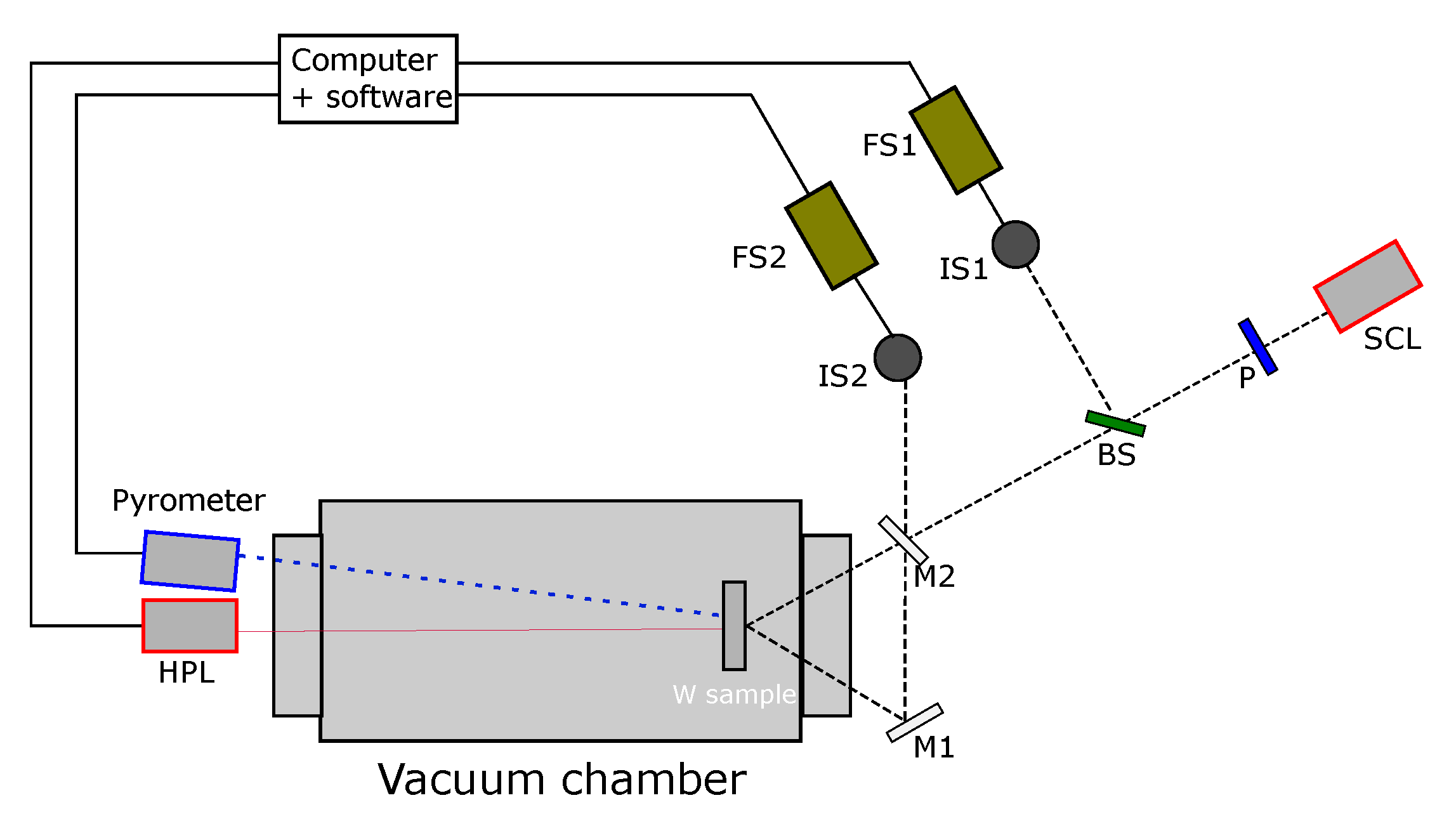
2. Materials and Methods

In the present work, we studied the optical properties of W as a function of temperature and roughness of five different samples. The polycrystalline 99.95 wt.% W samples ( 10 × 10 × 0.5 mm 3 , provided by GoodFellow) were mechanically polished in order to have a mirror-like surface. The roughness was controlled by etching four samples in Murakami’s solution [14] (i.e., a mixture of 10 wt.% KOH in H2O and 10 wt.% K3Fe(CN)6 in H2O) at different times. This method allows inducing a given roughness in the samples without bringing any mechanical damage. One of the five samples was left unetched and used as a reference; for the remaining four, we used etching times of 20, 40, 60, and 80 s, respectively. Just after etching, all samples were cleaned using an ultrasonic bath with acetone and ethanol.
The roughness of each sample was measured before and after laser annealing with atomic force microscopy (AFM, NT-MDT Spectrum Instruments) and confocal microscopy (CM, SENSOFAR), focusing approximately on the central area of the sample. Moreover, 40 × 40 µm 2 areas were scanned using AFM in a tapping mode with a resolution of 256 × 256 pixels. CM images have typical sizes of 1 × 0.75 mm 2 and were acquired using the 50 × objective, with a lateral resolution of 0.17 µm and a vertical resolution of less than 4 nm. Moreover, we performed an analysis of the elemental surface composition of the W sample before and after laser annealing using X-ray photoelectron spectroscopy (XPS). We used an experimental setup composed of a high-intensity Mg anode X-ray Source (PREVAC) emitting at 1253.6 eV. The analyzed samples were placed in a movable sample holder inside a mu-metal ultra-high vacuum chamber (base pressure 1 × 10 10 mbar). Photoelectrons were detected via a high-resolution electron energy analyzer (Scienta Omicron R3000) composed of a high transmission electron lens with an acceptance angle of 30 degrees and a 40 mm MCP detector monitored by a FireWire CCD camera. The resolution of the XPS spectrometer, determined from the full width at half maximum of the Ag 3d core levels of a clean Ag single crystal, was 0.9 eV [15].
The experimental setup used to perform optical measurements is presented in Figure 1. The reflectivity measurements were realized by varying the temperature of the sample from 25 to 800 °C. The samples were heated by using a continuous wave high-power laser (AMTRON, HPL in Figure 1), based on a fiber-coupled GaAs diode emitting at 805 nm, placed outside the vacuum chamber. The temperature of the sample wa controlled ex situ using a 1-color pyrometer (SensorTherm, model METIS M323) working in the 2–2.6 µm spectral range and allowing measurements of temperatures in the 50–800 °C range. Emissivity was set to 0.3 [16]. To limit surface contamination (e.g., oxidation) during laser annealing, the sample was placed in a sample holder made of Macor (a machinable glass-ceramic) inside a vacuum chamber (base pressure 5 × 10 8 mbar). Spectroscopic measurements were performed in the 500–1100 nm range. We used a supercontinuum white-light laser source (YSL Photonics, model SC-5, SCL in Figure 1) emitting 1.5 W in the 450–2400 nm range, with a fiber-collimated beam 1.5 mm in diameter. The SCL beam passed through a linear polarizer (ThorLabs, model LPVIS100-MP2 operating in the 550–1150 nm range) and reached a 70/30 beam splitter (ThorLabs, model BSS10, BS in Figure 1), which reflected 30% of the polarized beam to an integrating sphere made in Spectralon (LabSphere, IS1 in Figure 1) connected to a fiber spectrometer (Avantes, model AvaSpec-ULS2048L 200–1100 nm, FS1 in Figure 1) through a 1000 µm core fiber. The aim of this was to quantify the intensity fluctuations of the SCL laser arising from some non-linear mechanisms that allowed the creation of a supercontinuum, mainly dependent on the pumping noise. The SCL laser has relative stability of around 2%. The transmitted beam reaches either a removable reference silver mirror (ThorLabs, model PF05-03-P01, M2 in Figure 1), or the W sample. In the latter, the SCL beam crossed the silica window twice (before and after the W sample) and was sent to another integrating sphere (IS2) by means of a silver mirror (M1 in Figure 1).
The reflectivity recorded by FS2 was obtained by using the following equation:
R W , F S 2 ( λ ) = S m e a s ( λ ) S d a r k ( λ ) S r e f ( λ ) S d a r k ( λ ) 1 T w i 2 ( λ )
where S m e a s and S r e f are the spectra obtained by sending the SCL beam to the W sample or to the reference mirror M2, respectively; S d a r k is the dark spectrum obtained with the SCL source switched off and the sample set to the desired temperature with the HPL heating source on; T w i represents the transmission through the fused silica window. All reflectivity signals were then divided by the intensity signal S F S 1 recorded by the fiber spectrometer FS1, placed on the reference side and collecting the light reflected from the BS. The signal from FS2 (“sample-side” setup), in fact, carried information, not only on the interaction between SCL beam and samples, but also on the intrinsic intensity fluctuations of the SCL. The purpose of the “reference” side is to measure only such intrinsic fluctuations in real time, i.e., synchronized with the sample side. The corrected W reflectivity signal is then given by:
R W ( λ ) = R W , F S 2 ( λ ) S F S 1 ( λ , t = 0 ) S F S 1 ( λ , t )
where S F S 1 ( t ) is the signal recorded by FS1 at the generic time t when the SCL beam is sent on the sample, and S F S 1 ( t = 0 ) is the same signal recorded at the initial time when the SCL beam is sent on the reference mirror. For each sample, we performed spectroscopic measurements, keeping fixed the angle of incidence (with respect to the normal to the sample) at 30°, and changing the polarization of the SCL source (s and p polarization).
Each sample was heated using the following procedure: during a first temperature cycle, the sample was held for 5 min at 6 different temperatures (25, 200, 350, 450, 550, 650); a reflectivity measurement was performed for each temperature for both light polarizations. The sample was then annealed at 800 °C for 30 min. Reflectivity measurements were performed both at 800 °C and room temperature (≈25 °C) after cooling down. Two more identical annealing cycles were performed to study the evolution and the stability of the optical response of the sample. The purpose of the three temperature cycles, in fact, was to follow the change of reflectivity due to the temperature increase and the surface roughness/composition evolution. It is known that thermal annealing can be responsible for the evolution of surface roughness, as it induces stress liberation and structural improvement [17].

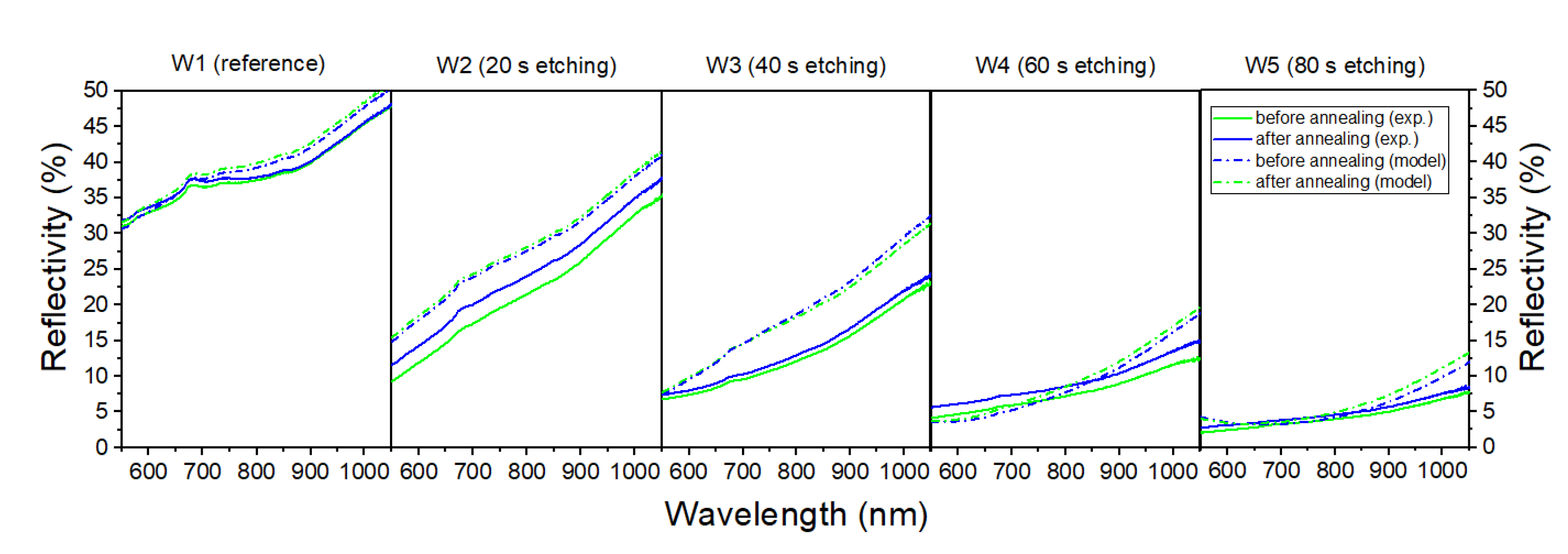
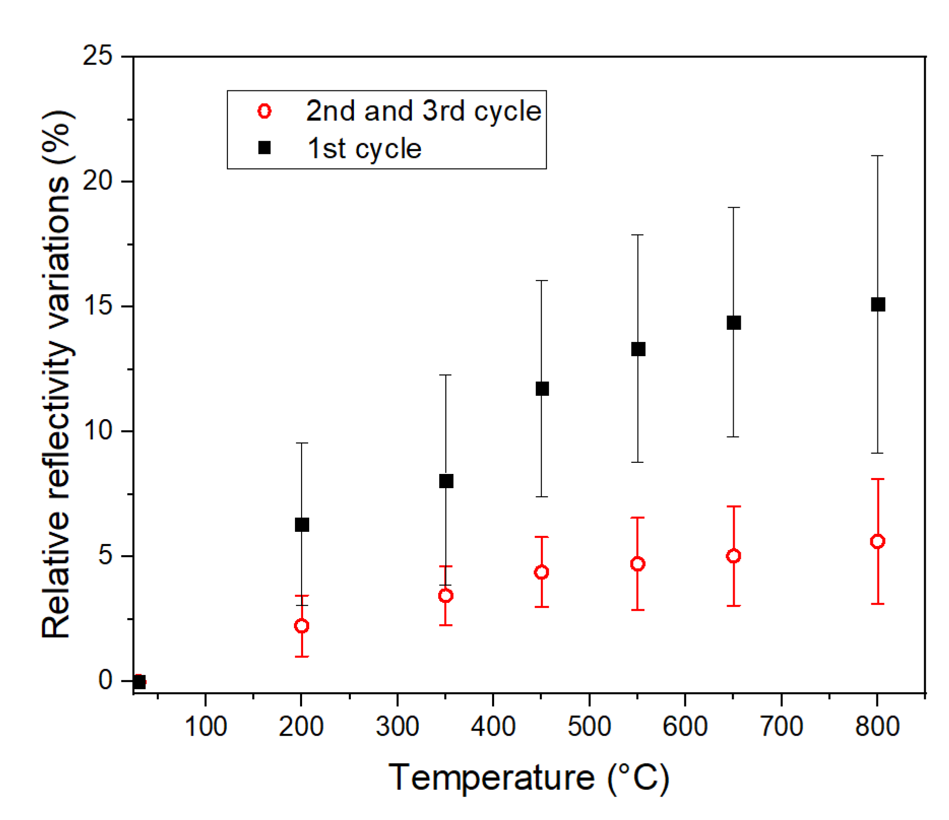
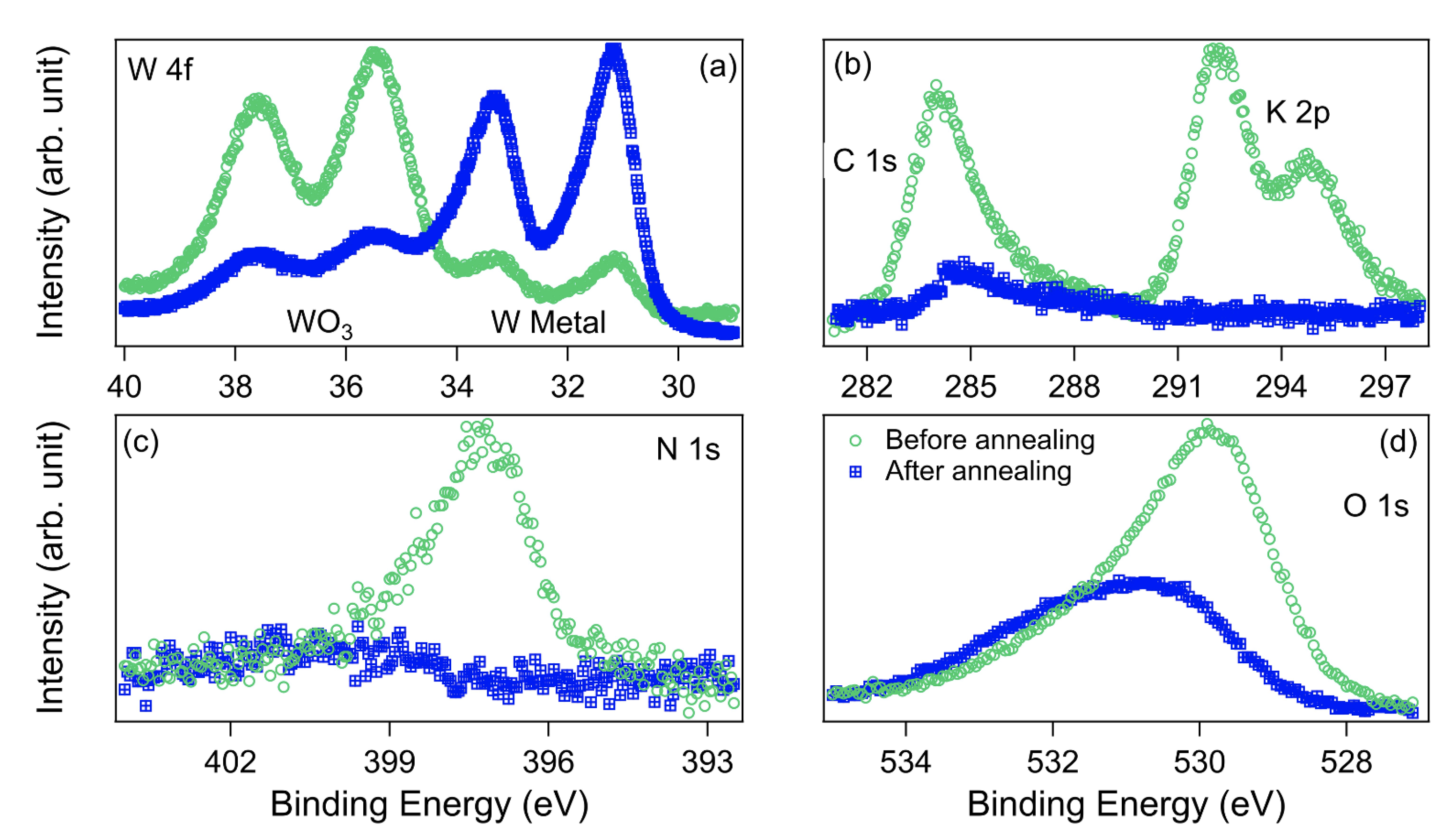
3. Results and Discussion

Here, we discuss the main results obtained to characterize the optical properties of W as a function of roughness and temperature, as well as the elemental and morphological evolution of the surface after laser-induced annealing.
We measured the RMS roughness for all samples before and after the annealing with both AFM and CM and found the values reported in Table 1. The uncertainties related to the σ values are the instrumental errors (20% of the measured value for AFM and 4 nm for CM). As an expected and desired effect of the chemical etching, the roughness of the samples (measured before the annealing) increases with etching time as:
σ = 20.8 + 0.93 × t e t c h i n g
Equation (3) was obtained from a linear fit of the experimental data, averaging the RMS roughness values obtained by both AFM and CM before the annealing. We can see that, after the heating procedure, roughness values measured by AFM did not follow a precise trend, apparently tending to homogenize, as they increased for samples with low-medium roughness (W1, W2, W3) and decreased for samples with higher roughness (W4, W5). AFM images of all samples before and after the annealing can be found in Figure S1 of the Supplementary Material. CM results, on the other hand, did not show relevant roughness variations after the heating. This was likely due to the fact that AFM values are representative only of the specific local area that is scanned.
In Figure 2, we present the reflectivity for the five samples before (green solid lines) and after (blue solid lines) the first laser annealing. In both cases, reflectivity spectra were recorded at room temperature. As expected, the reflectivity decreased when increasing the roughness, from 35% to 5% at 840 nm, from an RMS roughness ( σ hereafter) of 19 ± 4 nm to 86 ± 17 nm.
The dashed lines in Figure 2 are theoretical curves obtained using the relation derived by Bennett et al. [18], between reflectivity and σ :
R ( λ ) = R 0 ( λ ) e x p 4 π σ λ 2 + R 0 ( λ ) 2 5 π 4 m 2 σ λ 4 ( Δ θ ) 2
where R 0 is the reflectivity at the wavelength λ that the material would have if it was perfectly smooth, Δ θ is the instrumental acceptance angle and m is the root mean square slope of the profile of the surface, which depends on the autocovariance length a through the following relation: a = 2 σ / m . The first term refers to the specular reflectivity contribution, while the second term refers to the diffuse reflectivity contribution, which can be neglected when σ λ .
We used the σ values listed in Table 1 extracted from CM images before and after laser annealing; R 0 is the reflectivity curve of sample W1 (taken as a reference) and a is 1 µm. All the reflectivity curves are related to unpolarized light and were obtained by making an average of s and p polarization spectra.
The theoretical curves are in quite good quantitative agreement with experimental results. It can be observed that the theoretical curves of W3–W5 samples present spectral behavior slightly different from the experimental ones. A possible reason could be that the previous relation is valid only in the case that surface irregularities are much smaller compared to the used wavelength σ λ [18]. More accurate scattering models, considering the bidirectional reflection distribution function and, thus, overcoming the previous limitation, could provide a more accurate agreement between theoretical and experimental results [19], as shown in Minissale et al. [20] in the case of beryllium samples.
One can note in Figure 2 that, at room temperature, an irreversible increase of reflectivity is observed after the first annealing for all samples in the whole spectral range. Quantitatively, the irreversible relative increase of reflectivity measured at room temperature goes from 5% for the polished W1 sample to 10% for the rough W2 sample, which experienced the largest reflectivity change after the first annealing. However, we did not observe any irreversible evolution of the reflectivity at room temperature after the second and third annealing. In other words, after the second and third annealing, the reflectivity measured at room temperature was the same before and after each annealing.
Figure 3 shows the relative (with respect to room temperature) reflectivity variation at λ = 840 nm, averaged over the 5 samples, as a function of the sample temperature. The black squares represent the relative reflectivity variations during the first annealing. The variation ranges between 6% at 200 °C and 15% at the highest annealing temperature (800 °C). During the second annealing, we also observed a relative reflectivity variation, albeit smaller than in the first annealing. During the third annealing, the relative reflectivity variation was identical to the second annealing. During the second and third annealing, the largest reflectivity variation was around 6% at 800 °C, similarly to the value previously measured by Minissale et al. [21] on polished polycrystalline W, which was explained by the temperature-dependent electronic properties of W. Thus, the important reflectivity variation observed during the first annealing resulted from two different physical processes; the first one was related to the electronic properties of W and was reversible (such as in the second and third annealing), and the second one, which was irreversible, which we will address in the following paragraphs.
Two main hypotheses are considered to explain the variation during and after the first laser annealing: an evolution of the roughness or the composition of the surface. If one considers only roughness effects on reflectivity, an increase in roughness for a specific sample should correspond to a lower reflectivity spectrum, and vice versa. As discussed at the beginning of this section, roughness measurements do not show relevant roughness variations after the annealing. If surface roughness does not evolve significantly in the studied temperature range, it cannot explain the observed irreversible variation of reflectivity from the first annealing.
To test the second hypothesis (the evolution of the surface composition), we analyzed the elemental composition using XPS before and after the laser annealing. The different elements were assigned using the NIST-XPS database [22] and references therein. The core levels of the observed elements are shown in Figure 4 as a function of their binding energy for sample W5: (a) W 4f, (b) C 1s and K 2p, (c) N 1s, (d) O 1s. As seen in Figure 4a,d, the amount of tungsten oxide (WO 3 ), visible at 37.7 and 35.5 eV, was drastically reduced after laser annealing, while “bulk” metallic W peaks (at 33.3 and 31.1 eV) increased. WO 3 is a semiconductor with a band gap of 2.9 eV [23] absorbing for λ > 400 nm [24]. The increase of reflectivity in the visible and the near-infrared domains was likely related to the reduction of the natural oxide film, in agreement with Addab et al. [25], who studied the role of the thickness of oxide layers in decreasing the surface reflectivity in the 2.5–5.5 µm wavelength range. Moreover, as presented in Figure 4b,c, carbon, potassium, and nitrogen (chemical elements present in Murakami’s solution) are still present after ultrasonic cleaning for W2–W5 samples and could produce an additional absorption. The laser annealing, as in the case of WO 3 , allowed the desorption of such species. Thus, the reflectivity variation observed for all samples after the first annealing was likely due to two different contributions: the evolution of the native oxide and the desorption of residuals of the chemical etching solution. Since in W1, the only sample not etched, we did not detect any presence of potassium and nitrogen, but only an evolution of surface oxides (as observed by Pardanaud et al. [26]), the irreversible increase of reflectivity after the annealing could be attributed mainly to the evolution of surface oxides. We stress that tungsten oxides and carbon were systematically detected on all W samples, while the presence of potassium and nitrogen was clearly related to the used etching procedure.

4. Conclusions

In this study, we used chemical etching to control the surface roughness of tungsten in the 20–100 nm range and to study the role of morphology on the optical response of W. As expected, the measured reflectivity decreased when the surface roughness increased. A simple scattering model allowed quantitatively predicting the experimental findings and the evolution of reflectivity as a function of the surface roughness. Moreover, we followed the evolution of both the optical response and the surface morphology during laser annealing in the 25–800 °C temperature range. We observed that, during and after the annealing, reflectivity tended to increase for all samples. Using AFM and confocal microscopy techniques, we highlighted that evolution of RMS roughness could not be the origin of the measured reflectivity variation since roughness values did not sensibly vary in the investigated temperature range (25–800 °C). We demonstrated that the increase in reflectivity was rather due to a change in the chemical composition of the samples, performing a composition analysis (XPS) before and after the annealing. We observed that the heating caused the desorption of impurities (residuals of the etching solution) and reduced the amount of the native oxide, and we concluded that this last effect caused an increase in the specular reflection. Our findings are of particular interest to fusion technologies and tokamak reactors, since tungsten, thanks to its peculiar and useful properties, is suitable for environments where high photon and particle fluxes are present. By highlighting the role played by roughness and surface impurities (e.g., oxide), we provide insight into how W optical properties can evolve in harsh environments, where the presence of high ion fluxes, heat loads, and impurities can change both the morphology and surface composition of W.

Supplementary Materials

The following supporting information can be downloaded at: https://www.mdpi.com/article/10.3390/opt3030021/s1, Figure S1: AFM images of samples W1 (a, b), W2 (c, d), W3 (e, f), W4 (g, h), W5 (i, j), before (left) and after (right) the annealings; Figure S2: Relative reflectivity variation (with respect to room temperature measurement) at 600 nm (a) and 1000 nm (b) as a function of the samples temperature, during first annealing (black squares) and during second and third annealing (averaged, open red circles).

Author Contributions

Conceptualization, L.G., R.B. and M.M.; methodology, G.S. and M.M.; validation, F.P., G.S. and M.M.; formal analysis, M.M.; investigation, F.P., F.R.L. and C.L.d.C.; resources, C.M., L.G., R.B. and M.M.; data curation, F.P., F.R.L. and G.G.; writing—original draft preparation, F.P. and M.M.; writing—review and editing, F.R.L., C.M., G.G., G.S., E.S., T.A., L.G. and R.B.; visualization, F.P., E.S. and G.G.; supervision, L.G. and R.B.; project administration, M.M.; funding acquisition, C.M., T.A., L.G., R.B. and M.M. All authors have read and agreed to the published version of the manuscript.

Funding

This work was carried out within the framework of the French Federation for Magnetic Fusion Studies (FR-FCM) and of the EUROfusion Consortium, funded by the European Union via the Euratom Research and Training Programme (grant agreement no 101052200—EUROfusion). The views and opinions expressed are those of the author(s) only and do not necessarily reflect those of the European Union or the European Commission. Neither the European Union nor the European Commission can be held responsible for these views and opinions. The project leading to this publication has also received funding from the ANR under grants ANR-18-CE05-12 and ANR-20-CE08-0003-01.

Institutional Review Board Statement

Not applicable.

Informed Consent Statement

Not applicable.

Data Availability Statement

Data supporting the reported results can be found at ALADDIN (A Labelled Atomic Data INterface) repository (https://www-amdis.iaea.org/ALADDIN/, accessed on 2 April 2022).

Conflicts of Interest

The authors declare no conflict of interest. The funders had no role in the design of the study; in the collection, analyses, or interpretation of data; in the writing of the manuscript, or in the decision to publish the results.

References

  1. Gaspar, J.; Pocheau, C.; Corre, Y.; Ehret, N.; Guilhem, D.; Houry, M.; Loarer, T.; Loewenhoff, T.; Martin, C.; Pardanaud, C.; et al. Emissivity measurement of tungsten plasma facing components of the WEST tokamak. Fusion Eng. Des. 2019, 149, 111328. [Google Scholar] [CrossRef] [Green Version]
  2. Courtois, X.; Aumeunier, M.H.; Balorin, C.; Blanckaert, K.; Houry, M.; Jouve, M.; Moreau, P.; Pocheau, C.; Roche, H. Design and status of the new WEST IR thermography system. Fusion Eng. Des. 2018, 57, 1499–1504. [Google Scholar] [CrossRef]
  3. Aumeunier, M.H.; Kočan, M.; Reichle, R.; Gauthier, E. Impact of reflections on the divertor and first walls temperature measurements from the ITER infrared imaging system. Nucl. Mat. Energy 2017, 12, 1265–1269. [Google Scholar] [CrossRef]
  4. Brodu, E.; Balat-Pichelin, M.; Sans, J.L.; Kasper, J.C. Evolution of the emissivity of tungsten at high temperature with and without proton bombardment. Acta Mater. 2015, 84, 305–316. [Google Scholar] [CrossRef]
  5. Lott, F.; Netchaieff, A.; Escourbiac, F.; Jouvelot, J.L.; Constans, S.; Hernandez, D. Advances in optical thermometry for the ITER divertor. Fusion Eng. Des. 2010, 85, 146–152. [Google Scholar] [CrossRef]
  6. Balden, M.; Manhard, A.; Elgeti, S. Deuterium retention and morphological modifications of the surface in five grades of tungsten after deuterium plasma exposure. J. Nucl. Mat. 2014, 452, 248–256. [Google Scholar] [CrossRef] [Green Version]
  7. Gao, E.; Nadvornick, W.; Doerner, R.; Ghoniem, N.M. The influence of low-energy helium plasma on bubble formation in micro-engineered tungsten. J. Nucl. Mat. 2018, 501, 319–328. [Google Scholar] [CrossRef]
  8. Yang, Q.; Huang, Y.; Sun, J.; Liu, L.; Ni, W.; Fan, H.; Liu, D. Surface degeneration of tungsten wires irradiated with low-energy (12–220 eV) helium ions. Nucl. Inst. Meth. Phys. Res. 2018, 417, 48–52. [Google Scholar] [CrossRef]
  9. Ialovega, M.; Bernard, E.; Bisson, R.; Martin, C.; Sakamoto, R.; Kreter, A.; Hodille, E.; Angot, T.; Grisolia, C. Hydrogen trapping in tungsten: Impact of helium irradiation and thermal cycling. Phys. Scr. 2020, T171, 014066. [Google Scholar] [CrossRef]
  10. Martin, C.; Diez, M.; Campos, A.; Cabié, M.; Giacometti, G.; Balden, M.; Gallo, A.; Pegourié, B.; Bernard, E.; Tsitrone, E. First post-mortem analysis of deposits collected on ITER-like components in WEST after the C3 and C4 campaigns. Phys. Scr. 2021, 96, 124035. [Google Scholar] [CrossRef]
  11. Gaspar, J.; Corre, Y.; Rigollet, F.; Aumeunier, M.H.; Bernard, E.; Brezinsek, S.; Courtois, X.; Dejarnac, R.; Diez, M.; Dubus, L.; et al. Overview of the emissivity measurements performed in WEST: In-situ and post-mortem observations. Nucl. Fusions 2022. in print. [Google Scholar] [CrossRef]
  12. Kolasinski, R.D.; Wong, C.S.; Engel, A.; Whaley, J.A.; Allen, F.I.; Buchenauer, D.A. Deciphering the influence of high-flux helium plasma exposure on tungsten nanostructure growth using real-time, in situ spectroscopic ellipsometry. J. Appl. Phys. 2022, 131, 063303. [Google Scholar] [CrossRef]
  13. Bolt, H.; Barabash, V.; Federici, G.; Linke, J.; Loarte, A.; Roth, J.; Sato, K. Plasma facing and high heat flux materials-needs for ITER and beyond. J. Nucl. Mat. 2012, 43, 307–311. [Google Scholar] [CrossRef]
  14. Manhard, A.; Balden, M.; Von Toussaint, U. Blister formation on rough and technical tungsten surfaces exposed to deuterium plasma. Nucl. Fusion 2017, 57, 126012. [Google Scholar] [CrossRef] [Green Version]
  15. Salomon, E.; Minissale, M.; Lairado, F.R.; Coussan, S.; Rousselot-Pailley, P.; Dulieu, F.; Angot, T. Pyrene Adsorption on a Ag(111) Surface. J. Phys. Chem. C 2021, 125, 11166–11174. [Google Scholar] [CrossRef]
  16. Minissale, M.; Durif, A.; Hiret, P.; Vidal, T.; Faucheux, J.; Lenci, M.; Mondon, M.; Kermouche, C.; Pontillon, Y.; Grisolia, C.; et al. A high power laser facility to conduct annealing tests at high temperature. Rev. Sci. Instrum. 2020, 91, 035102. [Google Scholar] [CrossRef] [PubMed]
  17. Alonzo-Medina, G.M.; González-González, A.; Sacedón, J.L.; Oliva, A.I. Understanding the thermal annealing process for metallic thin films. IOP Conf. Ser. Mater. Sci. Eng 2013, 45, 012013. [Google Scholar] [CrossRef]
  18. Bennett, H.E.; Porteus, J. Relation between surface roughness and specular reflectance at normal incidence. Opt. Soc. Am. 1961, 51, 123–129. [Google Scholar] [CrossRef]
  19. Krywonos, A.; Harvey, J.E.; Choi, N. Linear systems formulation of scattering theory for rough surfaces with arbitrary incident and scattering angles. J. Opt. Soc. Am. A 2011, 28, 1121. [Google Scholar] [CrossRef]
  20. Minissale, M.; De Canonville, C.L.; Pardanaud, C.; Butoi, B.; Bisson, R.; Gallais, L. The role of defects, deuterium, and surface morphology on the optical response of beryllium. Nucl. Fusion 2022, 62, 056012. [Google Scholar] [CrossRef]
  21. Minissale, M.; Pardanaud, C.; Bisson, R.; Gallais, L. The temperature dependence of optical properties of tungsten in the visible and near-infrared domains: An experimental and theoretical study. J. Phys. D Appl. Phys. 2017, 50, 455601. [Google Scholar] [CrossRef] [Green Version]
  22. NIST. Available online: https://srdata.nist.gov/xps/main_search_menu.aspx (accessed on 8 June 2022).
  23. Johansson, M.B.; Zietz, B.; Niklasson, G.A.; Österlund, L. Optical properties of nanocrystalline WO3 and WO3-x thin films prepared by DC magnetron sputtering. J. Appl. Phys. 2014, 115, 213510. [Google Scholar] [CrossRef] [Green Version]
  24. Yoshimizu, M.; Hotori, Y.; Irie, H. Ohmic Hetero-Junction of n-Type Silicon and Tungsten Trioxide for Visible-Light Sensitive Photocatalyst. J. Mater. Sci. Chem. Eng. 2017, 5, 33–43. [Google Scholar] [CrossRef] [Green Version]
  25. Addab, Y.; Martin, C.; Pardanaud, C.; Khayadjian, J.; Achkasov, K.; Kogut, D.; Cartry, G.; Giacometti, G.; Cabié, M.; Gardarein, J.L.; et al. Formation of thin tungsten oxide layers: Characterization and exposure to deuterium. Phys. Scr. 2016, 167, 014036. [Google Scholar] [CrossRef]
  26. Pardanaud, C.; Dellasega, D.; Passoni, M.; Martin, C.; Roubin, P.; Addab, Y.; Arnas, C.; Couëdel, L.; Minissale, M.; Salomon, E.; et al. Post-mortem analysis of tungsten plasma facing components in tokamaks: Raman microscopy measurements on compact, porous oxide and nitride films and nanoparticles. Nucl. Fusion 2020, 60, 086004. [Google Scholar] [CrossRef]
Figure 1. Schematic of the experimental setup: HPL, high power laser; SCL, supercontinuum laser; P, polarizer; BS, beam splitter; M1 and M2, fixed and removable silver mirrors, respectively; IS1 and IS2, integrating spheres of reference and sample side, respectively; FS1 and FS2, fiber-optic spectrometers connected to IS1 and IS2, respectively.
Optics 03 00021 g001
Figure 2. Experimental reflectivity spectra measured at room temperature (solid lines) for unpolarized light before (green) and after laser annealing (blue), and theoretical curves (dashed lines) obtained with Equation (4).
Optics 03 00021 g002
Figure 3. Relative reflectivity variation (with respect to the RT curve) at 840 nm as a function of temperature, during the first annealing (black squares) and the second and third ones (averaged, open red circles). Each point was obtained by averaging over the five samples, the error bar being the standard deviation.
Optics 03 00021 g003
Figure 4. XPS spectra of sample W5 as a function of binding energy, showing the core levels of W 4f (a), C 1s and K 2p (b), N 1s (c), and O 1s (d) before (green open circles) and after annealing (blue squares).
Optics 03 00021 g004
Table 1. RMS roughness ( σ ) before and after annealing for the five studied samples, obtained from AFM and confocal measurements.
SampleEtching σ Before Annealing (nm) σ After Annealing (nm)
Time (s)AFMConfocalAFMConfocal
W1019 ± 416 ± 430 ± 619 ± 4
W22050 ± 1038 ± 463 ± 1338 ± 4
W34054 ± 1155 ± 461 ± 1255 ± 4
W46087 ± 1779 ± 462 ± 1284 ± 4
W58086 ± 1796 ± 484 ± 17102 ± 4
Publisher’s Note: MDPI stays neutral with regard to jurisdictional claims in published maps and institutional affiliations.

