Metal (Ag/Ti)-Containing Hydrogenated Amorphous Carbon Nanocomposite Films with Enhanced Nanoscratch Resistance: Hybrid PECVD/PVD System and Microstructural Characteristics

 ,
,
Abstract
:
1. Introduction
2. Materials and Methods
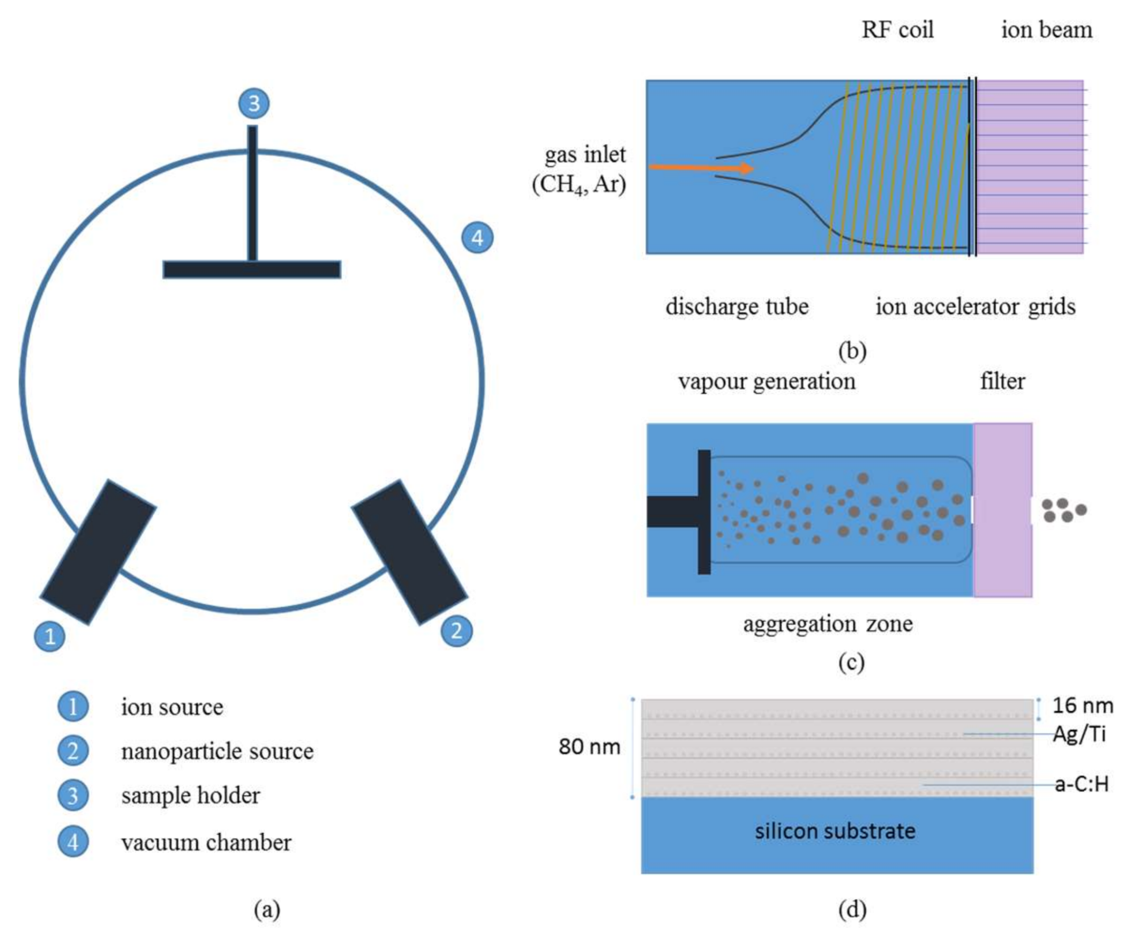
2.1. Deposition of Nanocomposite a–C:H:Me Films
2.1.1. Ion Beam Source
2.1.2. Nanoparticle Source
2.1.3. Hybrid Deposition of a–C:H:Me Nanocomposite Films
2.2. Characterization of Nanoparticles and Films
2.2.1. X-ray Reflectivity
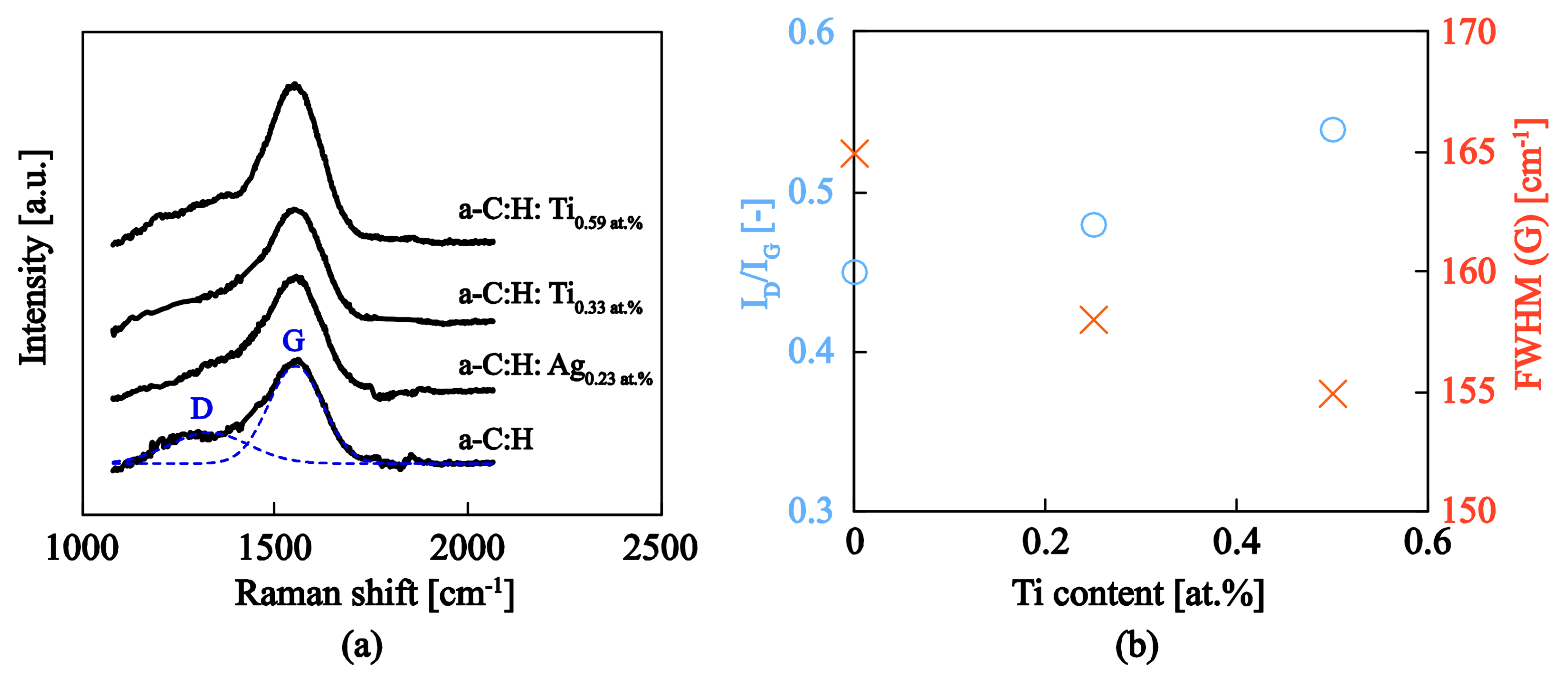
2.2.2. Raman Spectroscopy
2.2.3. Atomic Force Microscopy
2.2.4. Nanomechanical Testing
2.2.5. Transmission/Scanning Electron Microscopy
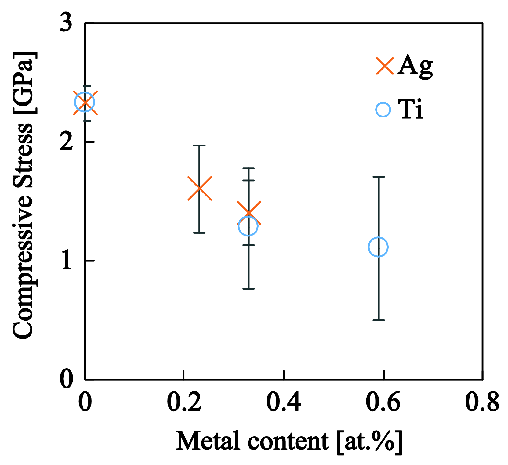
2.2.6. Residual Stress Measurements
3. Results and Discussion
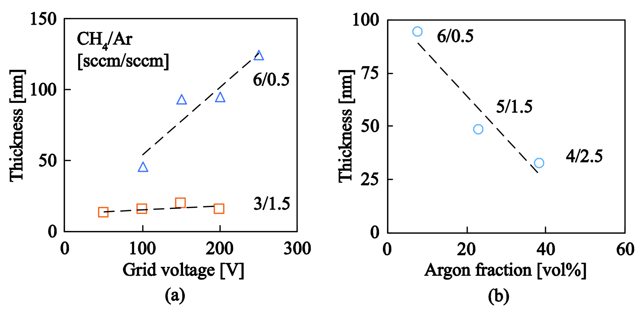
3.1. Ion Source and a–C:H Deposition Rate
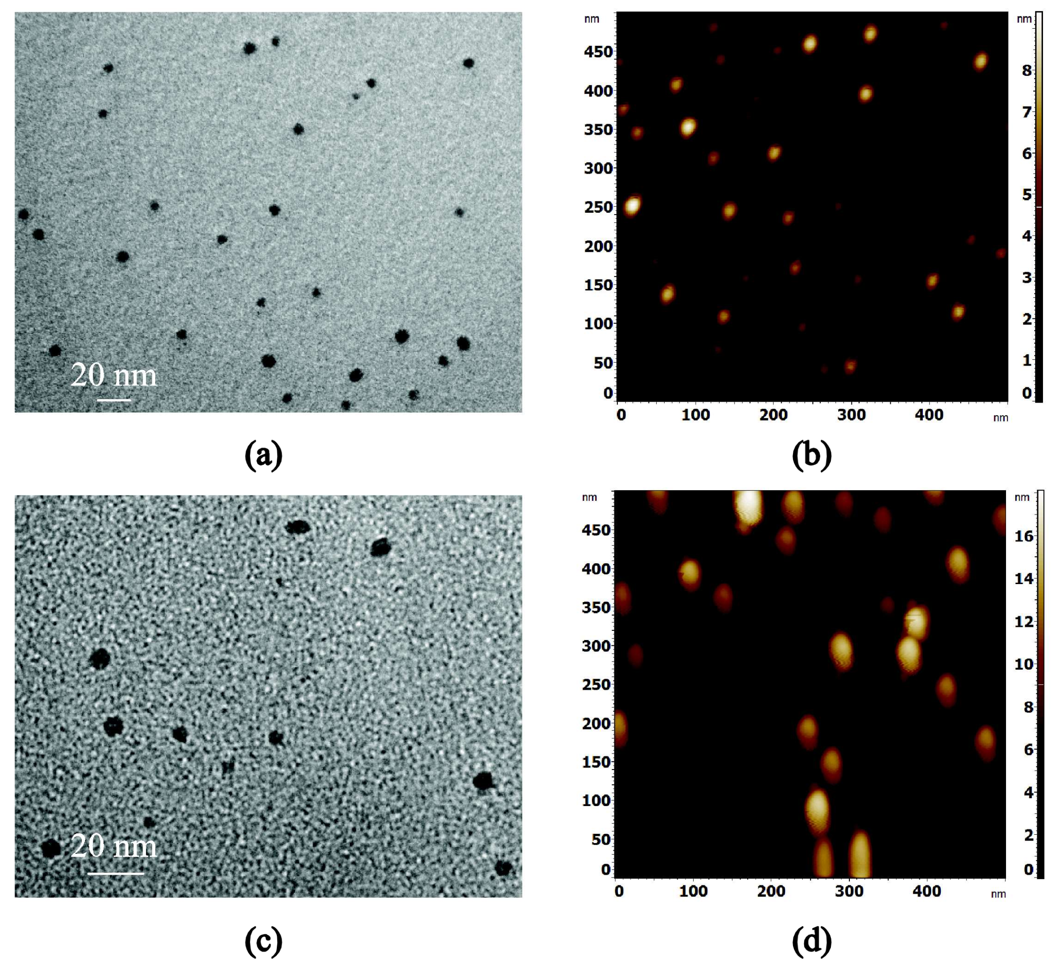
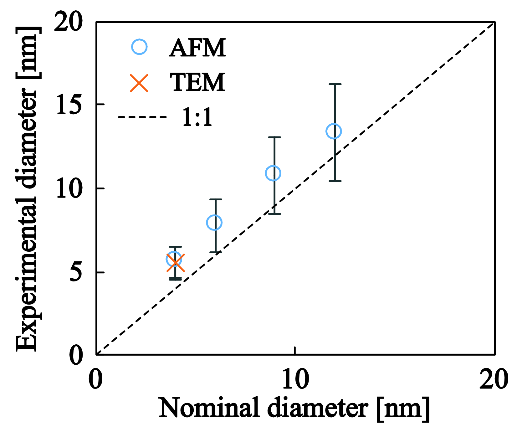
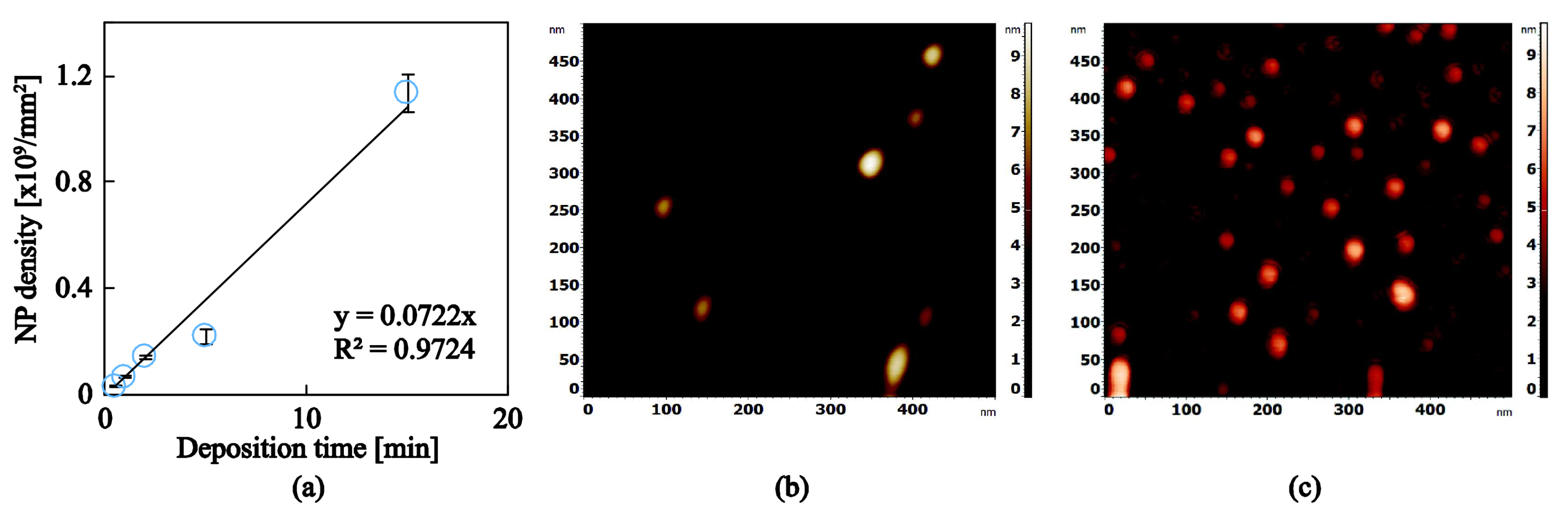
3.2. Ag and Ti Nanoparticles
3.3. a-C:H:Ag and a-C:H:Ti Nanocomposite Films
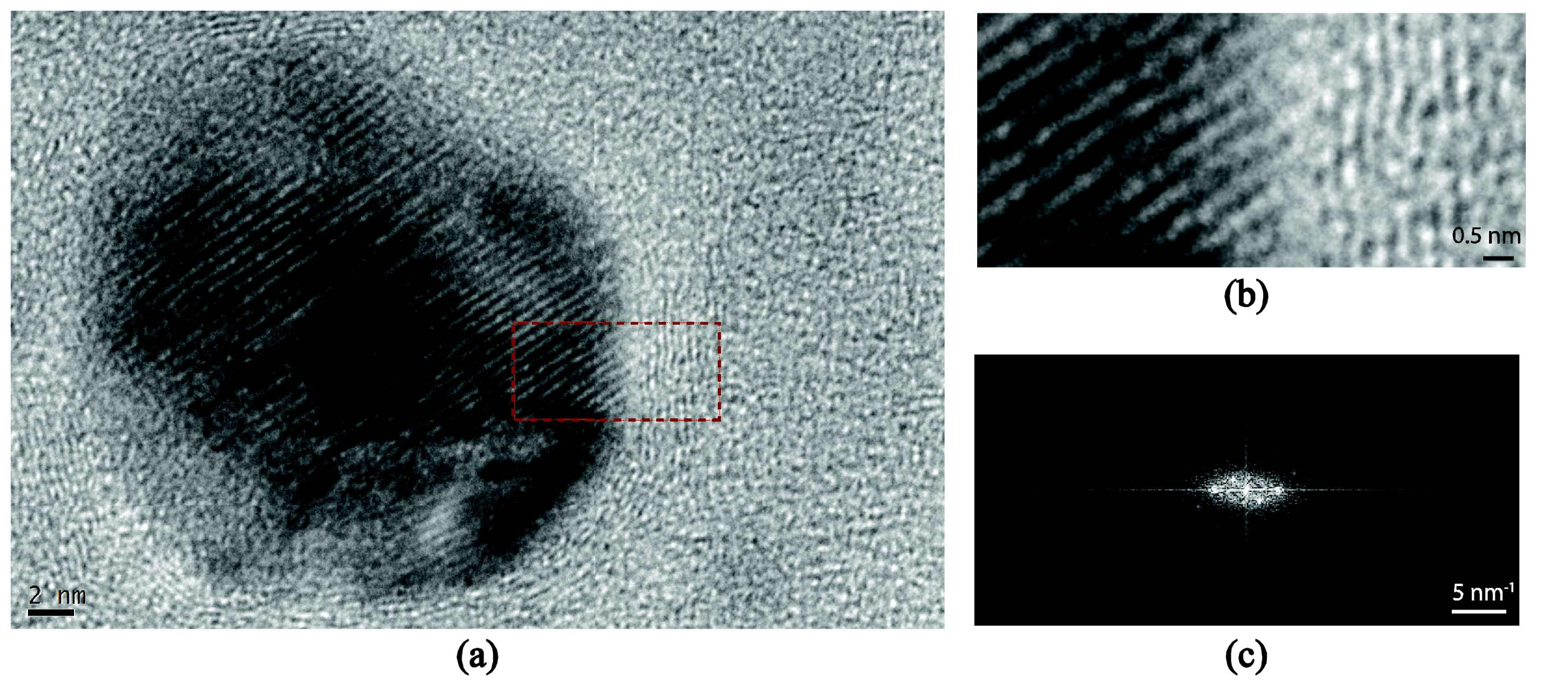
3.3.1. Microstructural Details and Bonding Characteristics
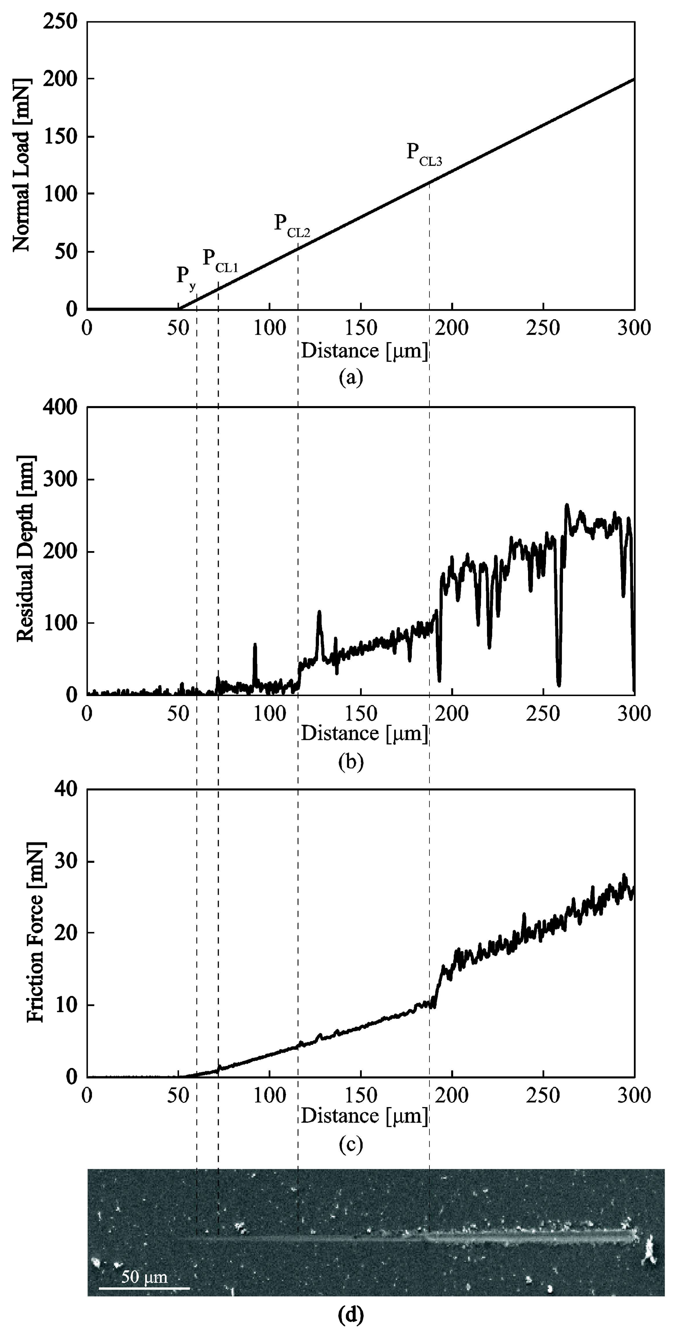
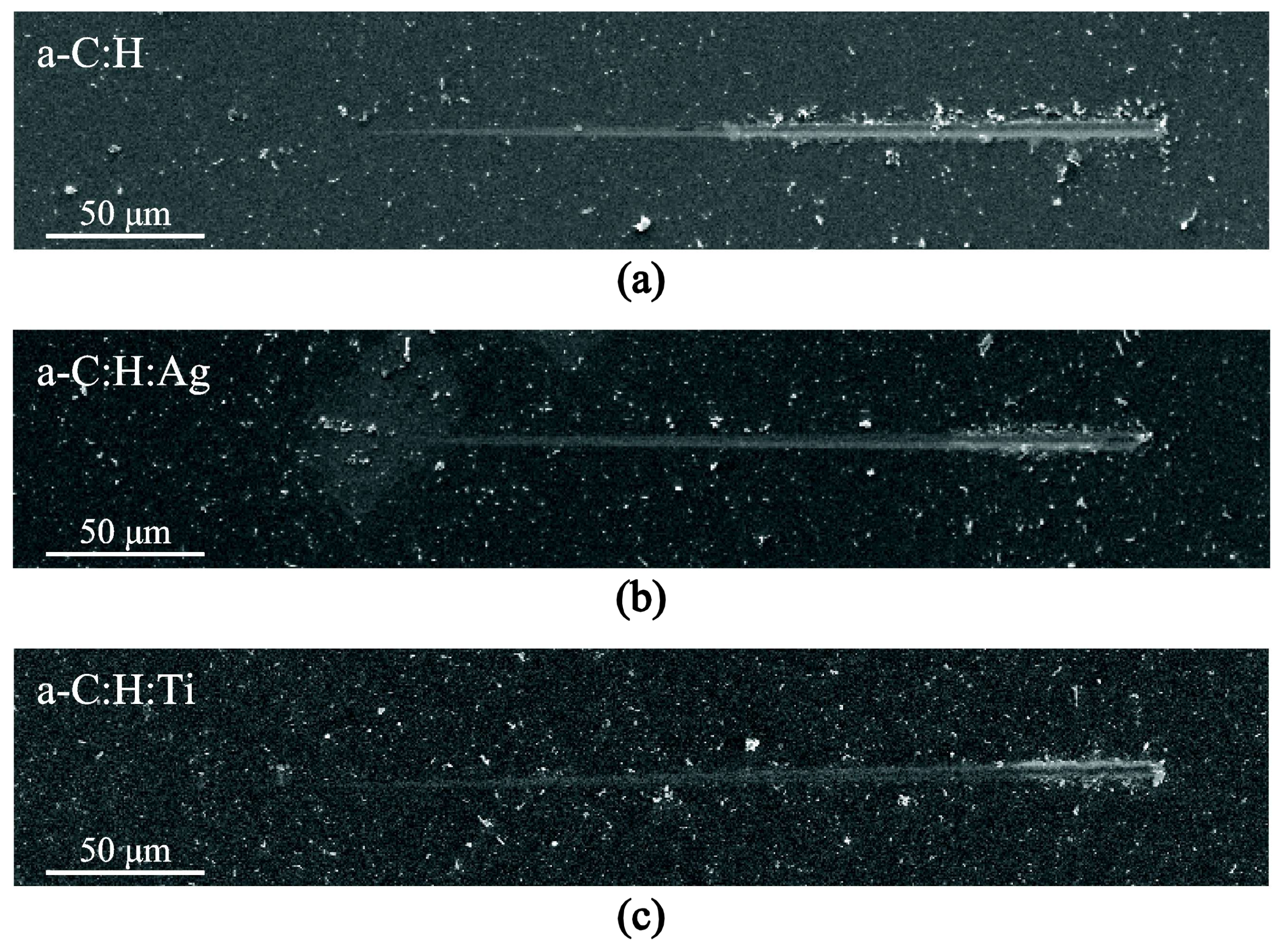
3.3.2. Nanotribological Response: Scratch Resistance and Friction Coefficient
4. Conclusions
Acknowledgments
Author Contributions
Conflicts of Interest
References
- Ferrari, A.C.; Robertson, J. Resonant Raman spectroscopy of disordered, amorphous, and diamondlike carbon. Phys. Rev. B 2001, 64, 75414. [Google Scholar] [CrossRef]
- Robertson, J. Properties of diamond-like carbon. Surf. Coat. Technol. 1992, 50, 185–203. [Google Scholar] [CrossRef]
- Robertson, J. Diamond-like amorphous carbon. Mater. Sci. Eng. R Rep. 2002, 37, 129–281. [Google Scholar] [CrossRef]
- Lifshitz, Y. Diamond-like carbon—Present status. Diam. Relat. Mater. 1999, 8, 1659–1676. [Google Scholar] [CrossRef]
- Robertson, J. Comparison of diamond-like carbon to diamond for applications. Phys. Status Solidi Appl. Mater. Sci. 2008, 205, 2233–2244. [Google Scholar] [CrossRef]
- Shirakura, A.; Nakaya, M.; Koga, Y.; Kodama, H.; Hasebe, T.; Suzuki, T. Diamond-like carbon films for PET bottles and medical applications. Thin Solid Films 2006, 494, 84–91. [Google Scholar] [CrossRef]
- Tsubone, D.; Hasebe, T.; Kamijo, A.; Hotta, A. Fracture mechanics of diamond-like carbon (DLC) films coated on flexible polymer substrates. Surf. Coat. Technol. 2007, 201, 6423–6430. [Google Scholar] [CrossRef]
- Lifshitz, Y.; Kasi, S.R.; Rabalais, J.W.; Eckstein, W. Subplantation model for film growth from hyperthermal species. Phys. Rev. B 1990, 41, 10468–10480. [Google Scholar] [CrossRef]
- Choi, H.W.; Choi, J.-H.; Lee, K.-R.; Ahn, J.-P.; Oh, K.H. Structure and mechanical properties of Ag-incorporated DLC films prepared by a hybrid ion beam deposition system. Thin Solid Films 2007, 516, 248–251. [Google Scholar] [CrossRef]
- Cui, J.; Qiang, L.; Zhang, B.; Ling, X.; Yang, T.; Zhang, J. Mechanical and tribological properties of Ti-DLC films with different Ti content by magnetron sputtering technique. Appl. Surf. Sci. 2012, 258, 5025–5030. [Google Scholar] [CrossRef]
- Tang, X.S.; Wang, H.J.; Feng, L.; Shao, L.X.; Zou, C.W. Mo doped DLC nanocomposite coatings with improved mechanical and blood compatibility properties. Appl. Surf. Sci. 2014, 311, 758–762. [Google Scholar] [CrossRef]
- Constantinou, M.; Pervolaraki, M.; Nikolaou, P.; Prouskas, C.; Patsalas, P.; Kelires, P.; Giapintzakis, J.; Constantinides, G. Microstructure and nanomechanical properties of pulsed excimer laser deposited DLC:Ag films: Enhanced nanotribological response. Surf. Coat. Technol. 2017, 309, 320–330. [Google Scholar] [CrossRef]
- Constantinou, M.; Pervolaraki, M.; Koutsokeras, L.; Prouskas, C.; Patsalas, P.; Kelires, P.; Giapintzakis, J.; Constantinides, G. Enhancing the nanoscratch resistance of pulsed laser deposited DLC films through molybdenum-doping. Surf. Coat. Technol. 2017, 330, 185–195. [Google Scholar] [CrossRef]
- Yamamoto, G.; Okabe, T.; Ikenaga, N. Fracture behavior of diamondlike carbon films deposited on polymer substrates. J. Vac. Sci. Technol. A Vac. Surf. Film 2018, 36, 02C101. [Google Scholar] [CrossRef]
- Baba, K.; Hatada, R.; Flege, S.; Ensinger, W.; Shibata, Y.; Nakashima, J.; Sawase, T.; Morimura, T. Preparation and antibacterial properties of Ag-containing diamond-like carbon films prepared by a combination of magnetron sputtering and plasma source ion implantation. Vacuum 2013, 89, 179–184. [Google Scholar] [CrossRef]
- Venkatesh, M.; Taktak, S.; Meletis, E.I. Characterization of nanocomposite a-C:H/Ag thin films synthesized by a hybrid deposition process. Phys. Met. Metallogr. 2015, 116, 781–790. [Google Scholar] [CrossRef]
- Wu, Y.; Chen, J.; Li, H.; Ji, L.; Ye, Y.; Zhou, H. Preparation and properties of Ag/DLC nanocomposite films fabricated by unbalanced magnetron sputtering. Appl. Surf. Sci. 2013, 284, 165–170. [Google Scholar] [CrossRef]
- Delmdahl, R. The excimer laser: Precision engineering. Nat. Photonics 2010, 4, 286. [Google Scholar] [CrossRef]
- Delmdahl, R.; Pätzel, R. Excimer laser technology trends. J. Phys. D Appl. Phys. 2014, 47, 34004. [Google Scholar] [CrossRef]
- Guler, U.; Shalaev, V.M.; Boltasseva, A. Nanoparticle plasmonics: Going practical with transition metal nitrides. Mater. Today 2015, 18, 227–237. [Google Scholar] [CrossRef]
- Zoubos, H.; Koutsokeras, L.E.; Anagnostopoulos, D.F.; Lidorikis, E.; Kalogirou, S.A.; Wildes, A.R.; Kelires, P.C.; Patsalas, P. Broadband optical absorption of amorphous carbon/Ag nanocomposite films and its potential for solar harvesting applications. Sol. Energy Mater. Sol. Cells 2013, 117, 350–356. [Google Scholar] [CrossRef]
- Nikolaou, P.; Mina, C.; Constantinou, M.; Koutsokeras, L.E.; Constantinides, G.; Lidorikis, E.; Avgeropoulos, A.; Kelires, P.C.; Patsalas, P. Functionally graded poly(dimethylsiloxane)/silver nanocomposites with tailored broadband optical absorption. Thin Solid Films 2015, 581. [Google Scholar] [CrossRef]
- Pauksch, L.; Hartmann, S.; Rohnke, M.; Szalay, G.; Alt, V.; Schnettler, R.; Lips, K.S. Biocompatibility of silver nanoparticles and silver ions in primary human mesenchymal stem cells and osteoblasts. Acta Biomater. 2014, 10, 439–449. [Google Scholar] [CrossRef] [PubMed]
- Greulich, C.; Braun, D.; Peetsch, A.; Diendorf, J.; Siebers, B.; Epple, M.; Köller, M. The toxic effect of silver ions and silver nanoparticles towards bacteria and human cells occurs in the same concentration range. RSC Adv. 2012, 2, 6981. [Google Scholar] [CrossRef]
- Castiglioni, S.; Cazzaniga, A.; Locatelli, L.; Maier, J.A.M. Silver Nanoparticles in Orthopedic Applications: New Insights on Their Effects on Osteogenic Cells. Nanomaterials 2017, 7, 124. [Google Scholar] [CrossRef] [PubMed]
- Barbasz, A.; Oćwieja, M.; Roman, M. Toxicity of silver nanoparticles towards tumoral human cell lines U-937 and HL-60. Colloids Surfaces B Biointerfaces 2017, 156, 397–404. [Google Scholar] [CrossRef] [PubMed]
- Necula, B.S.; Van Leeuwen, J.P.T.M.; Fratila-Apachitei, L.E.; Zaat, S.A.J.; Apachitei, I.; Duszczyk, J. In vitro cytotoxicity evaluation of porous TiO2-Ag antibacterial coatings for human fetal osteoblasts. Acta Biomater. 2012, 8, 4191–4197. [Google Scholar] [CrossRef] [PubMed]
- Vrcek, I.V.; Zuntar, I.; Petlevski, R.; Pavicic, I.; Sikiric, M.D.; Curlin, M.; Goessler, W. Comparison of In Vitro Toxicity of Silver Ions and Silver Nanoparticles on Human Hepatoma Cells. Environ. Toxicol. 2009, 24, 296–303. [Google Scholar] [CrossRef]
- Yang, Q.; Joyce, D.E.; Saranu, S.; Hughes, G.M.; Varambhia, A.; Moody, M.P.; Bagot, P.A.J. A combined approach for deposition and characterization of atomically engineered catalyst nanoparticles. Catal. Struct. React. 2015, 1, 125–131. [Google Scholar] [CrossRef]
- Parratt, L.G. Surface studies of solids by total reflection of X-rays. Phys. Rev. 1954, 95, 359–369. [Google Scholar] [CrossRef]
- Photiou, D.; Panagiotopoulos, N.T.; Koutsokeras, L.; Evangelakis, G.A.; Constantinides, G. Microstructure and nanomechanical properties of magnetron sputtered Ti−Nb films. Surf. Coat. Technol. 2016, 302, 310–319. [Google Scholar] [CrossRef]
- Casiraghi, C.; Ferrari, A.C.; Robertson, J. Raman spectroscopy of hydrogenated amorphous carbons. Phys. Rev. B 2005, 72, 085401. [Google Scholar] [CrossRef]
- Constantinides, G.; Silva, E.C.C.M.; Blackman, G.S.; Van Vliet, K.J. Dealing with imperfection: Quantifying potential length scale artefacts from nominally spherical indenter probes. Nanotechnology 2007, 18. [Google Scholar] [CrossRef]
- Stoney, G.G. The tension of metallic films deposited by electrolysis. Proc. R. Soc. A Math. Phys. Eng. Sci. 1909, 82, 172–175. [Google Scholar] [CrossRef]
- Guyot, N.; Harmand, Y.; Mezin, A. The role of the sample shape and size on the internal stress induced curvature of thin-film substrate systems. Int. J. Solids Struct. 2004, 41, 5143–5154. [Google Scholar] [CrossRef]
- Mezin, A. Coating internal stress measurement through the curvature method : A geometry-based criterion delimiting the relevance of Stoney’s formula. Surf. Coat. Technol. 2006, 200, 5259–5267. [Google Scholar] [CrossRef]
- Gelinas, V.; Vidal, D. Determination of particle shape distribution of clay using an automated AFM image analysis method. Powder Technol. 2010, 203, 254–264. [Google Scholar] [CrossRef]
- Gu, Y.; Xie, H.; Gao, J.; Liu, D.; Williams, C.T.; Murphy, C.J.; Ploehn, H.J. AFM characterization of dendrimer-stabilized platinum nanoparticles. Langmuir 2005, 21, 3122–3131. [Google Scholar] [CrossRef] [PubMed]
- Tritsaris, G.A.; Mathioudakis, C.; Kelires, P.C.; Kaxiras, E. Optical and elastic properties of diamond-like carbon with metallic inclusions: A theoretical study. J. Appl. Phys. 2012, 112, 103503. [Google Scholar] [CrossRef]
- Ferrari, A.C.; Robertson, J. Raman spectroscopy of amorphous, nanostructured, diamond-like carbon, and nanodiamond. Philos. Trans. A Math. Phys. Eng. Sci. 2004, 362, 2477–2512. [Google Scholar] [CrossRef] [PubMed]
- Ferrari, A.C.; Libassi, A.; Tanner, B.K.; Stolojan, V.; Yuan, J.; Brown, L.M.; Rodil, S.E.; Kleinsorge, B. Density, sp 3 fraction, and cross-sectional structure of amorphous carbon films determined by X-ray reflectivity and electron energy-loss spectroscopy. Phys. Rev. B 2000, 62, 11089–11103. [Google Scholar] [CrossRef]
- Meškinis, Š.; Vasiliauskas, A.; Šlapikas, K.; Niaura, G.; Juškenas, R.; Andrulevičius, M.; Tamulevičius, S. Structure of the silver containing diamond like carbon films: Study by multiwavelength Raman spectroscopy and XRD. Diam. Relat. Mater. 2013, 40, 32–37. [Google Scholar] [CrossRef]
- Ferrari, A.C.; Robertson, J. Interpretation of Raman spectra of disordered and amorphous carbon. Phys. Rev. B 2000, 61, 14095–14107. [Google Scholar] [CrossRef]
- Baba, K.; Hatada, R.; Flege, S.; Ensinger, W. Preparation and Properties of Ag-Containing Diamond-Like Carbon Films by Magnetron Plasma Source Ion Implantation. Adv. Mater. Sci. Eng. 2012, 2012, 536853. [Google Scholar] [CrossRef]
- Qiang, L.; Zhang, B.; Zhou, Y.; Zhang, J. Improving the internal stress and wear resistance of DLC film by low content Ti doping. Solid State Sci. 2013, 20, 17–22. [Google Scholar] [CrossRef]
- Huang, H.H.; Ho, C.T.; Lee, T.H.; Lee, T.L.; Liao, K.K.; Chen, F.L. Effect of surface roughness of ground titanium on initial cell adhesion. Biomol. Eng. 2004, 21, 93–97. [Google Scholar] [CrossRef] [PubMed]
- Zareidoost, A.; Yousefpour, M.; Ghaseme, B.; Amanzadeh, A. The relationship of surface roughness and cell response of chemical surface modification of titanium. J. Mater. Sci. Mater. Med. 2013, 23, 1479–1488. [Google Scholar] [CrossRef] [PubMed]
- Beake, B.D.; Harris, A.J.; Liskiewicz, T.W. Review of recent progress in nanoscratch testing. Tribol. Mater. Surf. Interfaces 2013, 7, 87–96. [Google Scholar] [CrossRef]
- Beake, B.D.; Davies, M.I.; Liskiewicz, T.W.; Vishnyakov, V.M.; Goodes, S.R. Nano-scratch, nanoindentation and fretting tests of 5–80 nm ta-C films on Si(100). Wear 2013, 301, 575–582. [Google Scholar] [CrossRef]
- Beake, B.D.; Vishnyakov, V.M.; Valizadeh, R.; Colligon, J.S. Influence of mechanical properties on the nanoscratch behaviour of hard nanocomposite TiN/Si 3 N 4 coatings on Si. J. Phys. D Appl. Phys. 2006, 39, 1392–1397. [Google Scholar] [CrossRef]
- Shi, B.; Sullivan, J.L.; Beake, B.D. An investigation into which factors control the nanotribological behaviour of thin sputtered carbon films. J. Phys. D Appl. Phys. 2008, 41, 45303. [Google Scholar] [CrossRef]
- Beake, B.D.; Goodes, S.R.; Shi, B. Nanomechanical and nanotribological testing of ultra-thin carbon-based and MoST films for increased MEMS durability. J. Phys. D Appl. Phys. 2009, 42, 65301. [Google Scholar] [CrossRef]
- Matenoglou, G.; Evangelakis, G.A.; Kosmidis, C.; Foulias, S.; Papadimitriou, D.; Patsalas, P. Pulsed laser deposition of amorphous carbon/silver nanocomposites. Appl. Surf. Sci. 2007, 253, 8155–8159. [Google Scholar] [CrossRef]
- Miyoshi, K. Adhesion, friction and micromechanical properties of ceramics. Surf. Coat. Technol. 1988, 36, 487–501. [Google Scholar] [CrossRef]
- Hamilton, G.M. Explicit equations for the stresses beneath a sliding spherical contact. Proc. Inst. Mech. Eng. 1983, 197C, 53–59. [Google Scholar] [CrossRef]
- Charitidis, C.A. Nanomechanical and nanotribological properties of carbon-based thin films: A review. Int. J. Refract. Met. Hard Mater. 2010, 28, 51–70. [Google Scholar] [CrossRef]
- Pardo, A.; Gómez-Aleixandre, C. Friction and Wear Behavior of Plasma Assisted Chemical Vapor Deposited Nanocomposites Made of Metal Nanoparticles Embedded in a Hydrogenated Amorphous Carbon Matrix. Surf. Coat. Technol. 2012, 206, 3116–3124. [Google Scholar] [CrossRef]
- Yu, X.; Qin, Y.; Wang, C.B.; Yang, Y.Q.; Ma, X.C. Effects of nanocrystalline silver incorporation on sliding tribological properties of Ag-containing diamond-like carbon films in multi-ion beam assisted deposition. Vacuum 2013, 89, 82–85. [Google Scholar] [CrossRef]
- Hatada, R.; Flege, S.; Bobrich, A.; Ensinger, W.; Dietz, C.; Baba, K.; Sawase, T.; Watamoto, T.; Matsutani, T. Preparation of Ag-containing diamond-like carbon films on the interior surface of tubes by a combined method of plasma source ion implantation and DC sputtering. Appl. Surf. Sci. 2014, 310, 257–261. [Google Scholar] [CrossRef]
- Erdemir, A.; Bindal, C.; Fenske, G.R.; Zuiker, C.; Wilbur, P. Characterization of transfer layers forming on surfaces sliding against diamond-like carbon. Surf. Coat. Technol. 1996, 86, 692–697. [Google Scholar] [CrossRef]


| Samples | Working Pressure (mbar) | Nominal Size (nm) | Deposition Time (s) | J (nA) | K (nA·s) |
|---|---|---|---|---|---|
| Ag12nm | 4.9 × 10⁻³ | 12 | 60 | 0.03 | 1.8 |
| Ag9nm | 4.8 × 10⁻³ | 9 | 18 | 0.10 | 1.8 |
| Ag6nm | 4.8 × 10⁻³ | 6 | 11 | 0.17 | 1.8 |
| Ag4nm | 4.8 × 10⁻³ | 4 | 45 | 0.04 | 1.8 |
| Samples | Working Pressure (mbar) | Nominal Size (nm) | Deposition Time (s) | J (nA) | K (nA·s) |
|---|---|---|---|---|---|
| Ag30s | 4.7 × 10⁻³ | 4 | 30 | 0.3 | 9 |
| Ag60s | 4.7 × 10⁻³ | 4 | 60 | 0.3 | 18 |
| Ag120s | 4.7 × 10⁻³ | 4 | 120 | 0.3 | 36 |
| Ag300s | 4.7 × 10⁻³ | 4 | 300 | 0.3 | 90 |
| Ag900s | 4.7 × 10⁻³ | 4 | 900 | 0.3 | 270 |
| Material | NP Size (nm) | Me Content (at.%) | RMS Roughness (nm) |
|---|---|---|---|
| - | 0 | 0.4 ± 0.1 | |
| 5.6 | 0.23 | 1.8 ± 1.0 | |
| 5.6 | 0.33 | 2.0 ± 0.6 | |
| 11.3 | 0.33 | 5.3 ± 0.9 | |
| 11.3 | 0.59 | 4.8 ± 0.2 |
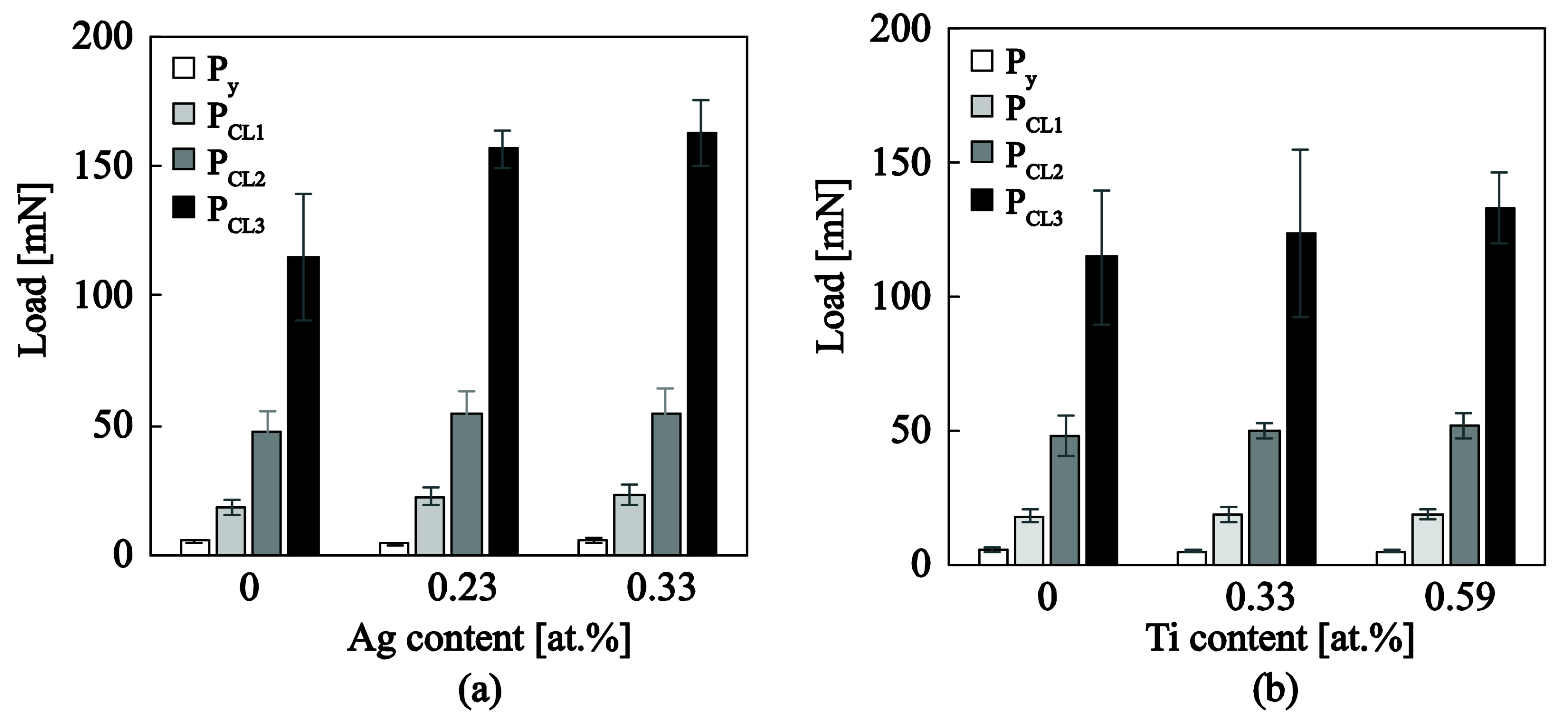
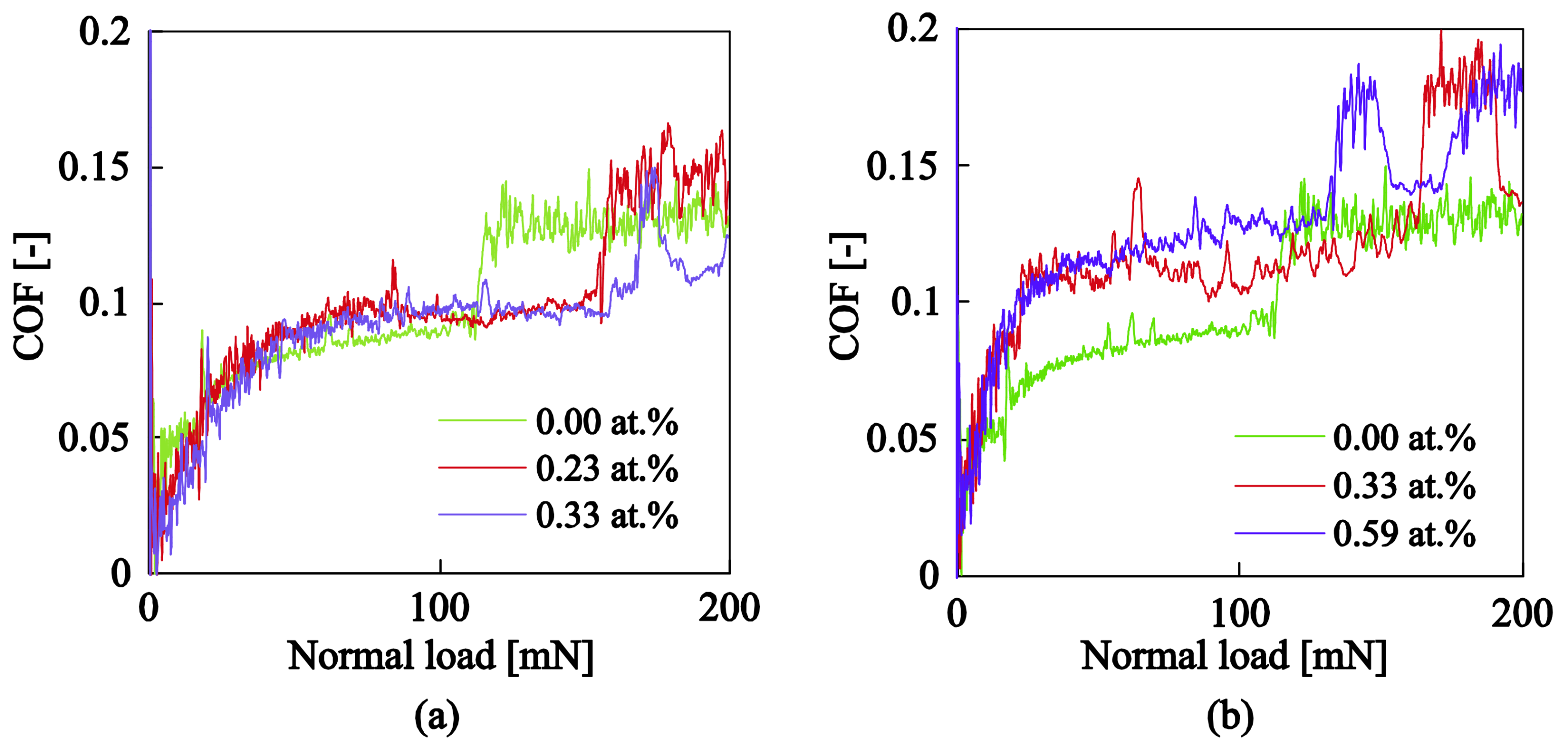
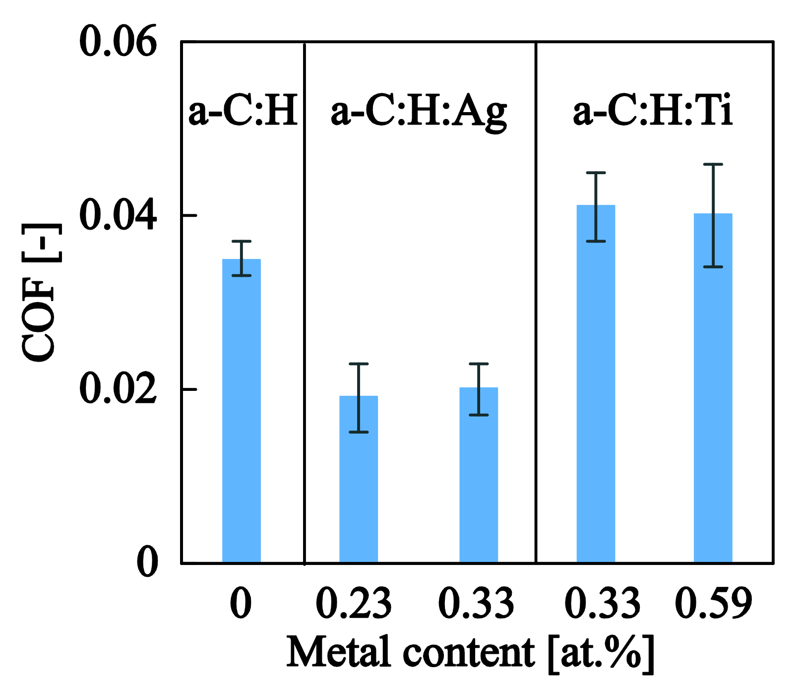
| Samples | (mN) | (mN) | (mN) | (mN) | COF (-) |
|---|---|---|---|---|---|
| a–C:H | 5.3 ± 0.6 | 18.2 ± 2.7 | 48.0 ± 7.7 | 114.8 ± 24.7 | 0.035 ± 0.002 |
| a–C:H:Ag0.23at.% | 4.5 ± 0.3 | 22.6 ± 3.7 | 54.2 ± 9.1 | 156.6 ± 7.5 | 0.019 ± 0.004 |
| a–C:H:Ag0.33at.% | 5.4 ± 0.7 | 23.5 ± 3.8 | 54.7 ± 9.3 | 162.8 ± 12.5 | 0.020 ± 0.003 |
| a–C:H:Ti0.33at.% | 4.7 ± 0.6 | 18.5 ± 2.9 | 49.8 ± 2.9 | 123.8 ± 31.5 | 0.041 ± 0.004 |
| a–C:H:Ti0.59at.% | 4.9 ± 0.4 | 18.8 ± 1.7 | 52.0 ± 5.0 | 133.0±13.1 | 0.040 ± 0.006 |
© 2018 by the authors. Licensee MDPI, Basel, Switzerland. This article is an open access article distributed under the terms and conditions of the Creative Commons Attribution (CC BY) license (http://creativecommons.org/licenses/by/4.0/).
Share and Cite
Constantinou, M.; Nikolaou, P.; Koutsokeras, L.; Avgeropoulos, A.; Moschovas, D.; Varotsis, C.; Patsalas, P.; Kelires, P.; Constantinides, G. Metal (Ag/Ti)-Containing Hydrogenated Amorphous Carbon Nanocomposite Films with Enhanced Nanoscratch Resistance: Hybrid PECVD/PVD System and Microstructural Characteristics. Nanomaterials 2018, 8, 209. https://doi.org/10.3390/nano8040209
Constantinou M, Nikolaou P, Koutsokeras L, Avgeropoulos A, Moschovas D, Varotsis C, Patsalas P, Kelires P, Constantinides G. Metal (Ag/Ti)-Containing Hydrogenated Amorphous Carbon Nanocomposite Films with Enhanced Nanoscratch Resistance: Hybrid PECVD/PVD System and Microstructural Characteristics. Nanomaterials. 2018; 8(4):209. https://doi.org/10.3390/nano8040209
Chicago/Turabian StyleConstantinou, Marios, Petros Nikolaou, Loukas Koutsokeras, Apostolos Avgeropoulos, Dimitrios Moschovas, Constantinos Varotsis, Panos Patsalas, Pantelis Kelires, and Georgios Constantinides. 2018. "Metal (Ag/Ti)-Containing Hydrogenated Amorphous Carbon Nanocomposite Films with Enhanced Nanoscratch Resistance: Hybrid PECVD/PVD System and Microstructural Characteristics" Nanomaterials 8, no. 4: 209. https://doi.org/10.3390/nano8040209