
Rapid Fabrication of Fe and Pd Thin Films as SERS-Active Substrates via Dynamic Hydrogen Bubble Template Method

Dipartimento di Chimica and Centro Interdipartimentale NIS (Nanostructured Interfaces and Surfaces), Università di Torino, Via Pietro Giuria 7, 10125 Torino, Italy
*
Author to whom correspondence should be addressed.
Nanomaterials 2023, 13(1), 135; https://doi.org/10.3390/nano13010135
Submission received: 7 November 2022
/
Revised: 20 December 2022
/
Accepted: 23 December 2022
/
Published: 27 December 2022
(This article belongs to the Special Issue Plasmonic Nanomaterials: Advances in Sensing Applications)
Abstract
:Fe and Pd thin film samples have been fabricated in a rapid fashion utilizing the versatile technique of dynamic hydrogen bubble template (DHBT) method via potentiostatic electrodeposition over a copper substrate. The morphology of the samples is dendritic, with the composition being directly proportional to the deposition time. All the samples have been tested as SERS substrates for the detection of Rhodamine 6G (R6G) dye. The samples perform very well, with the best performance shown by the Pd samples. The lowest detectable R6G concentration was found to be 10−6 M (479 μgL−1) by one of the Pd samples with the deposition time of 180 s. The highest enhancement of signals noticed in this sample can be attributed to its morphology, which is more nanostructured compared to other samples, which is extremely conducive to the phenomenon of localized surface plasmon resonance (LSPR). Overall, these samples are cheaper, easy to prepare with a rapid fabrication method, and show appreciable SERS performance.
1. Introduction
The preparation of materials that have both a high surface area and a precise and controlled morphology is of vital importance in many applications, in particular in sensors and in the field of catalysis in general [1,2,3]. The dynamic hydrogen bubble template (DHBT) method is quite attractive and has been proven to be excellent in that regard; it generates clean and porous structures in an efficient and rapid way in the absence of inorganic and organic templates [2]. In addition, it is highly controllable and “green” [4]. In DHBT, the working electrode is subjected to a cathodic potential that is within the H2 evolution range. The electrode surface experiences both H2 evolution and metal ion reduction simultaneously. Continuous gas nucleation, coalescence, and desorption at the electrode surface results in a self-supporting metallic thin film composed of nanoporous features. The size and the rate of evolution of hydrogen bubbles act as a dynamic template for depositing metal atoms, thus, generating porous materials with 3D “honeycomb” nanostructured architectures [5]. Such materials have found usage in a variety of applications, for example, Li batteries, capacitors, electrocatalysis, superhydrophobicity, and sensing applications [6,7,8,9,10,11,12,13,14,15,16].
Hydrogen gas bubble generation from the electrode surface involves three steps: nucleation, growth, and detachment. Application of high potentials leads to supersaturation of H2 close to the electrode, causing heterogeneous nucleation over the entire surface [17]. These bubbles tend to coalesce on the surface and increase in size until the contact angle is so small that they detach. At the same time as this phenomenon, however, the metal is discharging on the electrode surface. The bubbles are insulating, so through a surface-blocking effect, they reduce the effective surface area of the substrate, and therefore, the deposition occurs only in bubble-free areas, as originally observed directly by Tsai and collaborators [18,19]. When the bubbles detach from the surface of the substrate, those areas occupied by the bubbles remain empty. This allows the creation of a surface with a structure very particular, commonly called honeycomb, or the presence of developed dendrites vertically ensuring a high surface area. In fact, these bubbles act as a dynamic template during the process of electrodeposition, hence the name. The pores in the electrodeposited film will have approximately the same size as the diameter of the bubbles at the time of release, with the density of the pores of the film determined mainly by the behavior of the bubbles. The pore size increases with continued deposition because the bubbles have more time to coalesce and grow. The morphology of the metal film will depend on the mechanism of nucleation and metal growth, which depends on hydrodynamic conditions and on the potential applied during electrodeposition.
Some key parameters can be identified that affect the final structure of the deposited material: potential (or current density); source and concentration of H+ (acid or NH4Cl); substrate material, shape, and size; presence of surfactants and additives; chemical concentration/solution of metal salts; deposition time; and operating temperature. [20,21,22]. The material of the substrate should not generate too vigorous of an evolution of hydrogen that it does not allow a correct deposition of the metal and prevents the film from growing with an ordered microstructure. Copper is a great option since it guarantees adequate hydrogen evolution, not excessively intense. Cu has been frequently used as a substrate for the preparation of 3D-porous structures along with other metals [23]. It is possible to carry out this electrodeposition, as reported in the literature, also on others surfaces including evaporative films [12], laminae [24], microelectrodes, fine wires, discs [13], or electrodes silk-screened [25] and in all these substrates, the typical honeycomb structured morphology was obtained. The addition of any surfactants or additives can profoundly influence the behavior of the bubbles. There are many reagents that can be added to modify the surface morphology of the electrodeposited metal. Halides are common examples, including NaCl [26], HCl [27], NaBr [28], and NH4Cl [29]. Deposition time is also one of the most important variables to take into consideration when synthesizing via DHBT. The material, shape, size, and orientation of the working electrode can also influence the behavior of the bubble. The composition of the electrodeposited film can be readily adapted by altering the operational parameters and concentration of the bath of deposition. Bimetallic surfaces can also be obtained through the deposition of a metal through DHBT on top of a substrate consisting of another metal, which is then prepared by this technique [30]. The DHBT method, therefore, appears extremely interesting because it can quickly and efficiently deposit on both mono- and bimetallic surfaces.
Some of the syntheses and preparations of metal surfaces through DHBT are worth mentioning because they allowed the discovery and evolution of this technique. Co is among the most studied metals with a “honeycomb” structure; much of this work was carried out by Popovic, Nikolìc, and colleagues, which showed clear evidence of the bubble modeling effect of H2 [31,32]. Furthermore, Cu has been used extensively as a model for understanding nucleation and metal growth mechanisms via DHBT, leading to a good understanding of its behavior during the deposition [33]. Cherevko’s work demonstrated that honeycomb Ag structures can be easily formed using NH4Cl as a source of protons for the formation of H2 bubbles instead of an acid [34,35]. This work showed that noble metals could be synthesized with similar macroporous architectures and nanoscale characteristics, such as Cu and Ni, thus, generating desirable materials for a wide variety of applications. Depositions of other metals via DHBT were also investigated, such as Au [36], Pd [37], Ru [38], Bi [39], and Pt [12]. M. Asnavandi and C. Zhao used DHBT electrodeposition to prepare thin Ag, Pd, and Ni films [40]. A platinum film with the typical honeycomb structure was also prepared [41]. Cherevko and collaborators also studied the electrodeposition of Pb, while Huang and collaborators studied porous Sn [42,43].
Surface-enhanced Raman scattering is an incredibly useful technique that involves significant enhancement of Raman signals of analyte molecules adsorbed on nanostructured metal surfaces called substrates [44]. Although the mechanism behind the SERS enhancement has been associated with both electromagnetic and chemical effects, the former is much more widely acknowledged as the dominant effect. When the frequency of the incident electromagnetic radiation matches with that of surface conduction electrons (called surface plasmons) of the nanostructured plasmonic substrate, collective electron oscillations occur which cause an increase in the local electric field around sharp tips, edges, nanopores and interparticle gaps of the substrate—this phenomenon is called localized surface plasmon resonance [45]. Resultantly, it leads to enhancement of the Raman signals [46,47,48]. The nanostructured surface also gives rise to “hotspots”, i.e., places of giant electric field enhancement, which amplify the Raman signals to extremely high levels [49,50]. SERS offers diverse potential applications, including environmental monitoring, bio-analyses, forensic analyses, food quality control, material characterizations, etc. [51,52,53,54,55]. Credited to its remarkable sensitivity and enhancement factor as high as 1011, SERS technique can enable single-molecule level detection [56,57,58]. Cheap and convenient portable Raman spectrometers have been coupled with commercial SERS substrates, making SERS a promising analytical technique [44,59,60,61]. An array of nanomaterials with tailored morphologies have been utilized as efficient SERS substrates, credited to several decades of research and advancement in nanotechnology [62,63]. Yet the development of highly sensitive SERS substrates remains crucial and vital to widen the utility of SERS further.
Roughened precious metal surfaces, i.e., Ag, Au, and Cu, have been established to show strong SERS enhancement. But a lack of other active substrates has severely reduced the range of applications of SERS. Previously, FePd alloy has been reported to show impressive SERS performance with its high refractive index [56,64]. Palladium has good surface stability and finds ample utilization in electrochemistry as catalyst. Prior attempts have been introduced surface roughening on Pd to make it a SERS-active substrate, but more studies are still needed [65,66,67]. On the other hand, Fe is generally considered to be SERS-inactive, but numerous studies have displayed its appreciable activity towards SERS due to the lightning-rod effect, which involves huge electromagnetic enhancement at sharp features or high curvature sites, by virtue of their morphology and density [64,68,69,70,71,72,73,74,75,76]. In addition, Fe is a good choice dictated by economic and sustainability reasons, it is not a critical raw material, being abundantly present on earth and does not represent a risk either for the environment or health. Hence, testing out the individual metals for SERS is the aim of this paper. Monometallic thin films of Fe and Pd with high surface areas have been electrodeposited onto copper substrates via the Dynamic Hydrogen Bubble Template method. The as-deposited films have been characterized through the use of SEM, EDS and X-ray techniques. The as-deposited films have been tested as SERS-active substrates and showed impressive performance.
2. Materials and Methods
A copper tape was opted as the substrate of 0.5 mm thickness and 0.6 cm width, cut in different lengths depending on the characterization that would subsequently be performed on each of the samples. These substrates, as observed under the electron microscope, exhibit a surface that is not perfectly smooth. The observed roughness can certainly provide preferential sites for the production of bubbles and therefore affect the final structure of the films. From a practical point of view, this did not present a problem on the microstructures obtained, as will be discussed later with the images collected for the different samples. On one of the two faces (the one where there was an adhesive conductive tape), an insulating tape was applied so as to deposit the films in the same way every time and make the measurement the most reproducible. Once the substrate was prepared, it was washed in deionized water, then in ethanol, and again in deionized water and left to air dry for at least one day before carrying out the deposition. Electrolytic solutions were formulated from information present in the literature. The electrolyte used to deposit iron consisted of 0.1 M ferric sulfate heptahydrate (Fe2(SO4)3·7H2O) as the source of iron and 1.5 M ammonium chloride (NH4Cl) as a proton source, which is commonly used during electrodepositions via DHBT [77]. To deposit palladium, the electrolyte was composed of 0.1 M tetraamminepalladium chloride [Pd(NH3)4Cl2] and 1.5 M NH4Cl. A three-electrode cell setup connected to the Autolab potentiostat (Metrohm, Utrecht, The Netherlands) was used to prepare the samples. Platinum grid acted as the counter electrode, Ag/AgCl electrode as the reference in double-bridge configuration loaded with saturated solution of KCl and the conductive substrate of copper was the working electrode. The substrate was always immersed in the electrolyte solution vertically, reaching the maximum possible depth (without touching the bottom of the beaker). Electrodeposition was achieved at a constant potential of −4 V. The deposition times were 90, 180, and 300 s for each electrolyte. All syntheses were carried out at room temperature. Once the deposition was carried out for the predetermined time, the sample was washed in deionized water and left to dry in sample tubes. The as-deposited samples have been referred to as Fe90s, Fe180s, Fe300s, Pd90s, Pd180s, and Pd300s (the number in each name denotes the time of deposition in seconds). Then, the extra part of copper that served as contact with the clamp (therefore, not immersed in the electrolytic solution) was eliminated along with the initial part of the deposited film (approx. 1 cm) in order to avoid the possibility of nonhomogeneity of the film that can occur in this area that is closer to the solution/atmosphere interface.
The samples were weighed before and after each deposition, and the weight of the deposited film was determined. Since each deposition appeared uniform, the surface density in g/cm2 was also calculated for each sample by dividing the measured weight by the area of the substrate. These samples were then subjected to a morphological and structural characterization using SEM (Inspect SEM, FEI) (FEI, Hillsboro, OR, USA) equipped with an EDS probe (Oxford Ultim-Max 100) (Oxford Instruments, Abingdon, UK), a Panalytical X-pert X-ray Diffractometer in Bragg–Brentano geometry (Panalytical, Almelo, The Netherlands), and an Autolab potentiostat (the same as used in the preparation of the samples). The XRD peaks were indexed with the use of X’Pert Highscore software (version 2.2c (2.2.3.)).
A Renishaw inVia Raman Microscope (Renishaw, Wotton-under-Edge, England) with 514 nm laser line was used for SERS measurements, which were carried out in rotating mode [78]. The rotating sample platform allows the sample to be presented to the SERS detector in a continuous manner, minimizing background corrections and sample adjustment time [79]. A small value of standard deviation has been found, which reinforces the fact that the rotating mode allows for more reproducible and consistent measurements. The following conditions of measurements were applied: 20 s acquisition time, 20 × ULWD objective, and 0.095 mW laser power at the sample. Rhodamine 6G (R6G) dye was used as the probe molecule. The sample preparation involved cleaning the substrate in concentrated HNO3 for 5 min followed by rinsing with de-ionized water for several times. Then the sample was immersed in solution of Rhodamine 6G dye in de-ionized water of concentrations 10−3 M, 10−4 M, 10−6 M, 10−8 M, 10−10 M, and 10−12 M for 15 min in order to allow the probe molecules to be adsorbed at the sample surface. All solutions were prepared with chemical-grade reagents and de-ionized water. Air-drying and measuring the sample surface followed.
3. Results and Discussion
Thin films of pure Pd and Fe were deposited via DHBT electrodeposition. Each of the prepared samples was characterized using SEM, EDS, and XRD techniques. The characterization stage is fundamental to understanding if the properties that will be determined later for the different samples are characteristics of the deposited material or if the quantity of porous film is so low that the measurements were instead performed on the copper substrate.
3.1. Copper Substrate
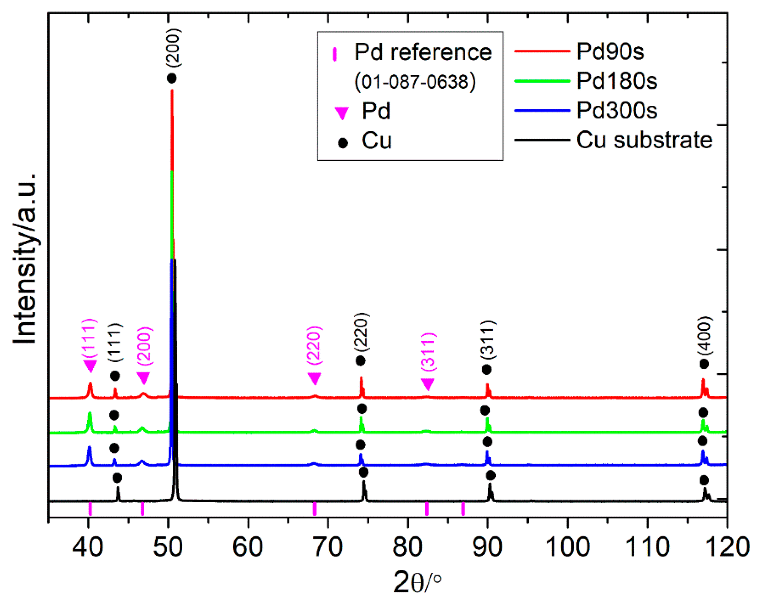
The surface of the substrate was analyzed through SEM, and from the image in Figure S1 of the supplementary material; it is evident that the copper strip has suffered a lamination process during production to make it thinner. In fact, there are clearly visible lines on the surface of the metallic tape (formed during rolling), all of which are parallel to each other and have a thickness within the micrometer range. The EDS investigation confirmed that the material is composed entirely of Cu (99.98%), confirming the specifications on the commercial conductive tape box. It is also important to record the XRD diffractogram of the copper substrate since in case the thickness of the deposited films via DHBT is not too high, X-rays are often able to penetrate through the film to the substrate and then return to peaks corresponding to the substrate material. Having a diffractogram of a blank copper substrate allows one to obtain an analog to the one in analytical chemistry called “white”, so as to easily distinguish the peaks generated by the Cu substrate from the peaks belonging to the as-deposited material. Figure 1 shows the diffractogram obtained from the copper tape (denoted in black) [80]. By increasing the deposition time, the blank reflections were shifted progressively to the left. This has to be considered an artifact due to the instrumental conditions of the Bragg-Brentano XRD and the thickness of the deposited layers; as the latter increases with the deposition time, the line source no longer remains coplanar with the z-axis of the Cu substrate, and thus, the resulting pattern shows left-shifted peaks.
3.2. Electrodeposition of Iron
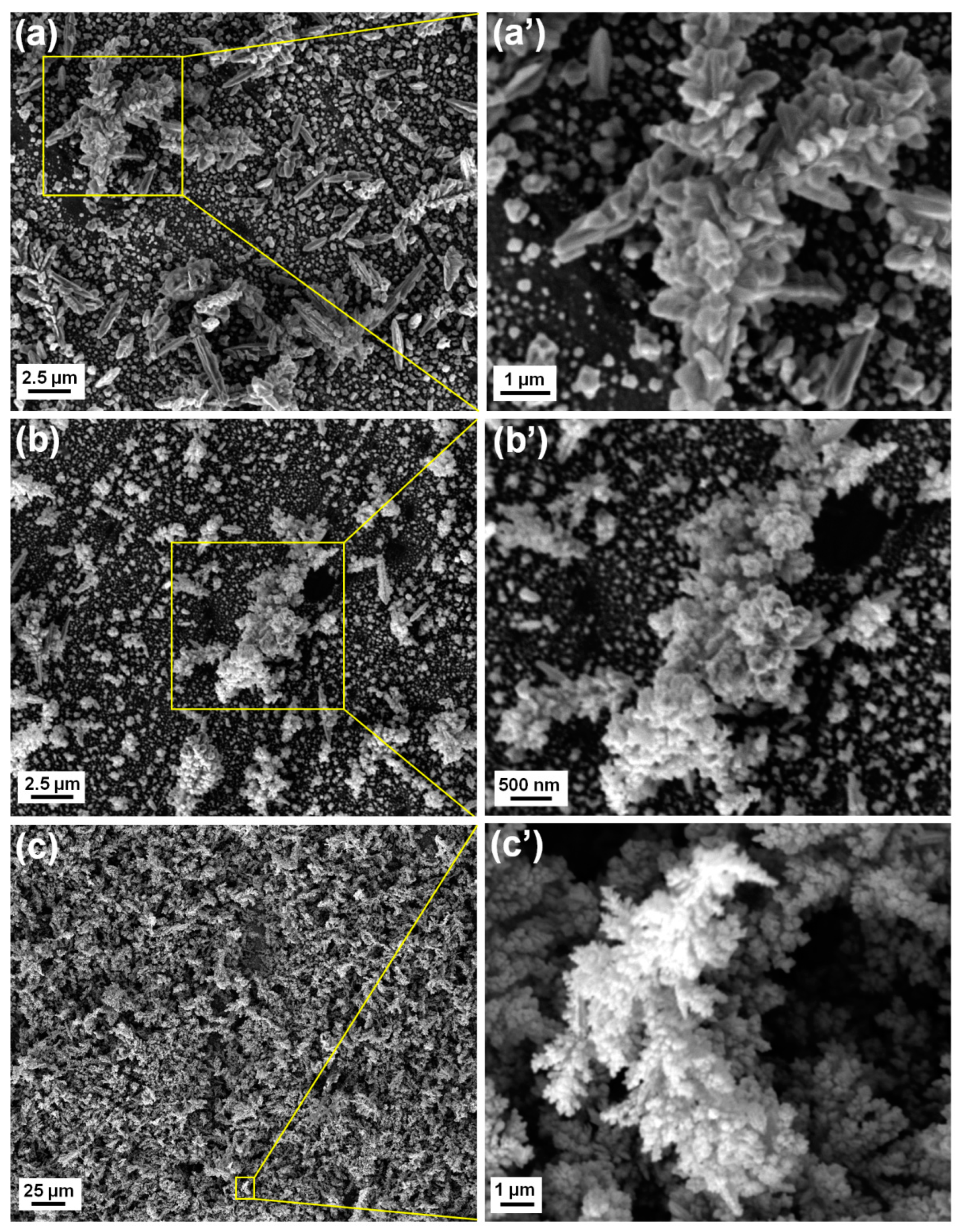
Firstly, thin films of Fe have been electrodeposited. As found in the literature, the most common conditions to perform DHBT electrodeposition in a potentiostatic setting involve applying a potential between −3 and −5 V (both potentials are negative enough to get out of the stability range of the solvent, water). Based on this observation, a potential of −4 V was chosen as the deposition potential in this case [81,82]. The potential indeed has a profound influence on the rate of metal deposition at the electrode and on the development of hydrogen, and therefore, on the final structure possessed by the samples. Figure 2 shows the SEM images of the surfaces of the electrodeposited Fe samples. The obtained structure is not of the honeycomb type, and only a small amount of Fe deposition has been achieved. EDS confirmed the presence of Fe, as expected. As the deposition time increases, the microstructure changes; in fact, the images (a) and (b) in Figure 2 show a less compact dendritic-type growth, while in (c), the metal possesses a structure more similar to that of particles deposited on the surface. At higher magnification, the dendritic growth can be observed more closely (Figure 2a’–c’). With the increasing deposition time, the dendrites undergo a gradual development from being in clusters as in the case of Fe90s, to taking up a flower-like shape and morphology seen for Fe180s and eventually acquiring the most defined shape visible in Fe300s. The deposited Fe amount increases with increasing deposition time; this suggests that the longer deposition time results in the substrate acquiring enhanced coverage while a lesser surface area remains exposed to be detected by the beam limited by its depth of penetration.
The XRD diffractograms of the substrate and the as-deposited samples are displayed in Figure 1. The samples show all peaks of Cu with an additional peak of bcc Fe (110) (denoted by the pink triangle). The peak positions of Cu have been shifted to the left as a result of layers of deposited Fe, which increased the overall thickness of the sample. On the other hand, peaks of Fe maintain their position since their position is always the same, i.e., on top of the sample. Other iron peaks are not clearly visible; only the most intense peak is seen, probably because the deposition layer was too thin. Additionally, there are no peaks attributable to iron oxides. Based on these results, it is clear that mainly metallic Fe has been deposited on the copper substrate.
3.3. Electrodeposition of Palladium
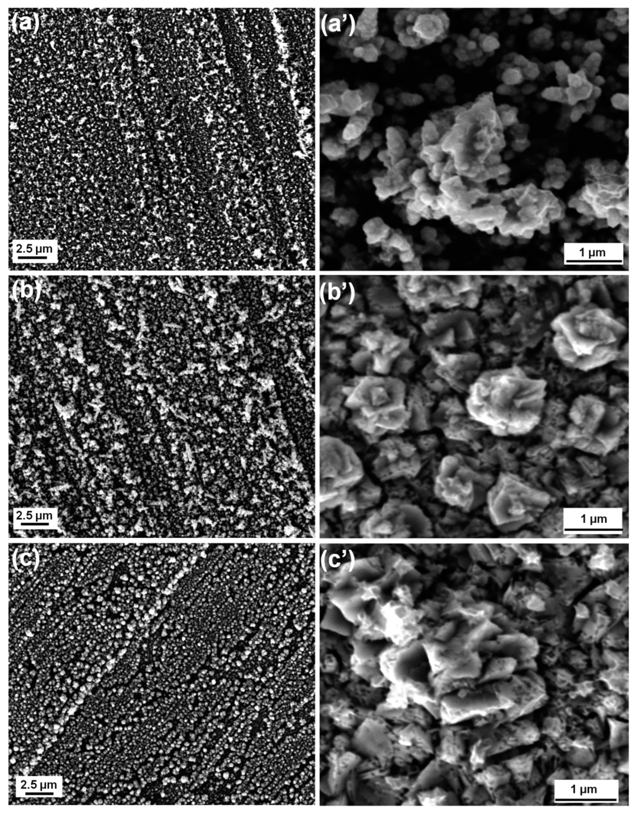
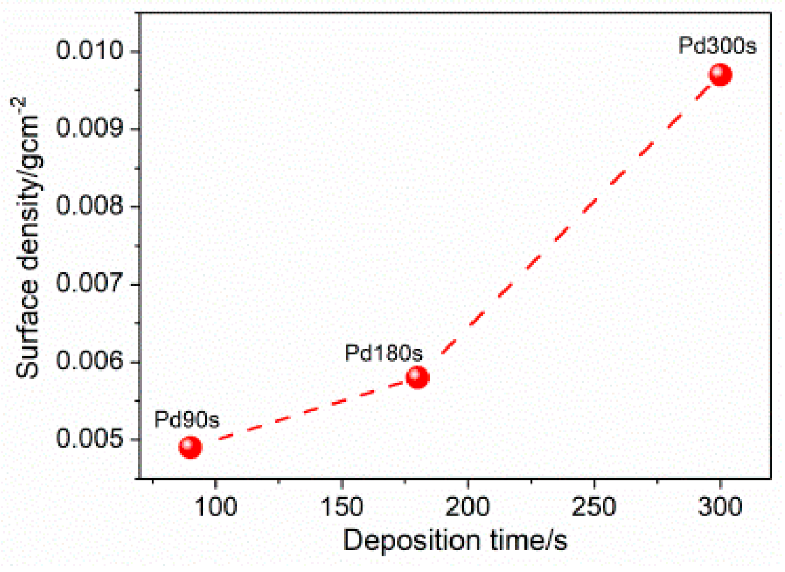
Figure 3 shows the XRD pattern for the as-deposited samples. The representative peaks for pure Pd are apparent, along with the peaks associated with the Cu substrate. From this diffractogram, it is possible to draw qualitative considerations about the whole. The SEM images obtained for the different samples have been provided in Figure 4. By observing the images from top to bottom in the order of increasing deposition time, it provides the idea that as the deposition time increases, the quantity of metal that is discharged at the electrode is always greater and the coverage becomes progressively dense. This is most evident, particularly in Pd300s, while the differences are less obvious between Pd180s and Pd90s. There is an obvious presence of dendrites in Pd90s (Figure 4a) that are randomly spread over the entire sample surface. With an increase in deposition time, i.e., for Pd180s (Figure 4b), the dendrites continue to grow and start to occupy more surface area. Eventually, in Pd300s (Figure 4c), they can be seen to be ubiquitous throughout the sample surface. Notably, the conditions of deposition do not lead to a well-organized honeycomb-like structure. The SEM images in Figure 4a’–c’ allow seeing the growing dendrite more closely. The morphology of the dendrites appears with a more classic shape with many lateral ramifications. The composition of Pd90s, Pd180s, and Pd300s was checked by EDS, and just Pd was detected predictably. The densities of the materials deposited for Pd90s, Pd180s, and Pd300s were found to be 0.0049, 0.0058, and 0.0097 g/cm2, respectively. Figure 5 shows the relationship between the surface density of the Pd samples and the deposition times, and it is clear that the surface density increases with increasing deposition time.
3.4. SERS Measurements
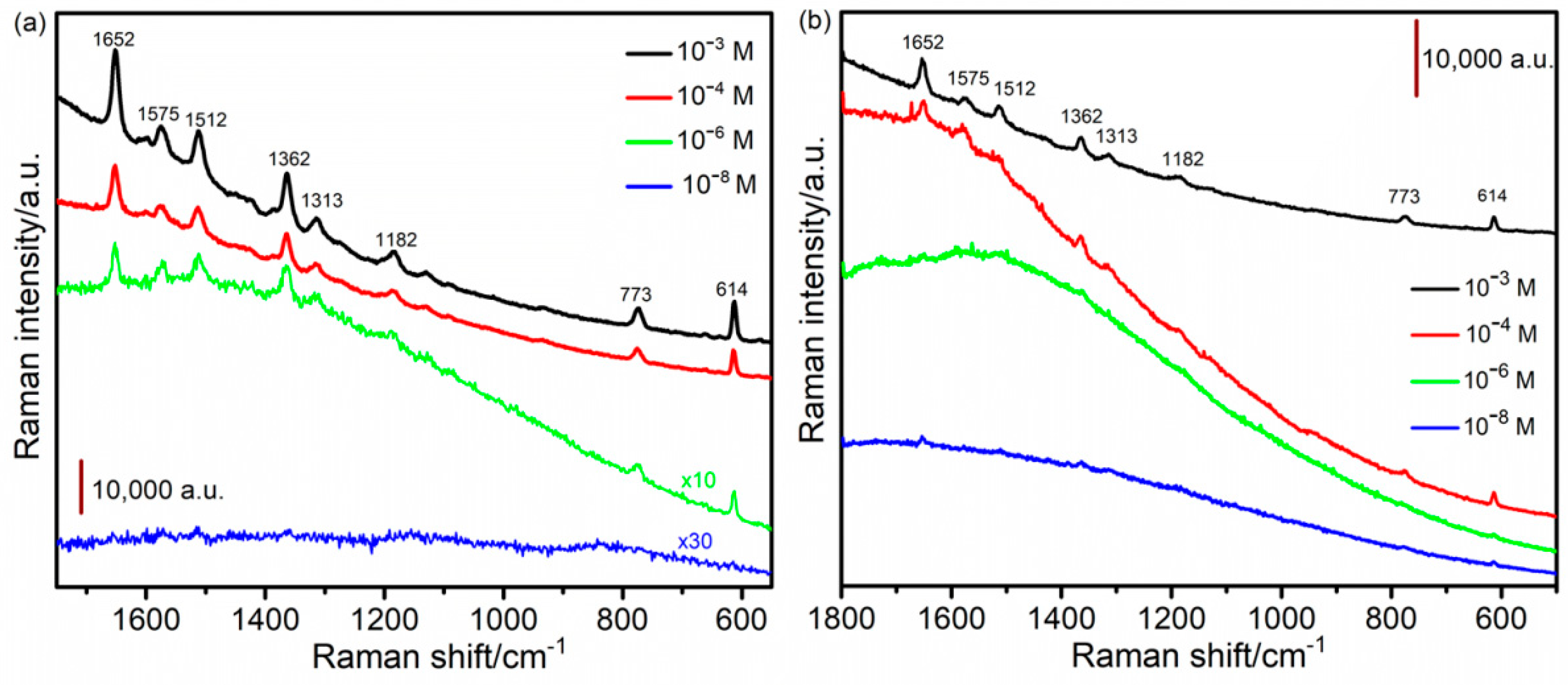
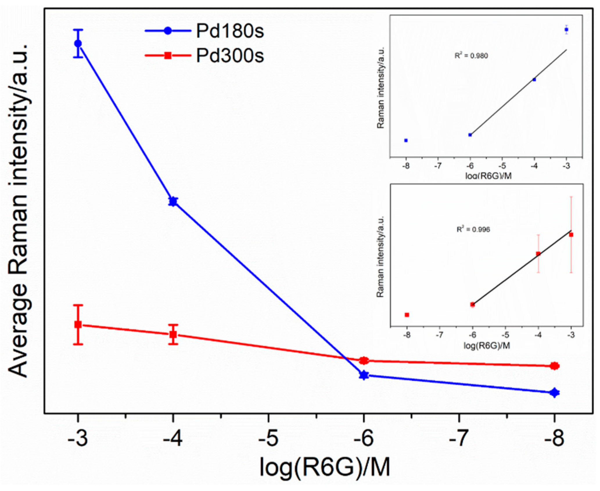
The as-prepared thin film samples were employed as a SERS substrate for detection of the probe molecule, Rhodamine 6G dye (R6G). Solutions of R6G in de-ionized water were prepared with different concentrations, i.e., 10−3 M, 10−4 M, 10−6 M, 10−8 M, and 10−10 M. The samples were immersed in each solution for 15 min, air-dried, and then, subjected to the SERS measurements. Figure 6a,b display the spectra obtained for Pd180s, Pd300s, and Fe180s, respectively. The representative peaks of the probe molecule are shown by all the three mentioned samples at 1652 cm−1, 1575 cm−1, 1512 cm−1, 1362 cm−1, 1313 cm−1, 1182 cm−1, 773 cm−1 and 614 cm−1 shown. The nanostructured substrate surface with nanogaps between the interconnected dendrites is believed to be the key factor behind the SERS performance attributed to the electromagnetic enhancement effect [83]. In the case of Pd180s (Figure 6a), the signals are very evident at a low concentration of 10−3 M until 10−6 M, after which the signals are not clear at 10−8 M. Hence, 10−6 M (479 μgL−1) is the lowest possible R6G concentration that could be detected by the sample, Pd180s. This limit of detection is comparable to those previously reported for R6G, e.g., amorphous semiconducting rhodium sulfide microbowl substrates and 2D titanium carbide (MXene) [84,85]. Similarly, Pd300s in Figure 6b continue to show signal enhancement from 10−3 M R6G, decreasing in intensity until 10−8 M. Despite being a lesser SERS-active metal than Pd, Fe180s reveals appreciable performance with apparent signal enhancement and a low detection limit of 10−6 M (as shown in Figure S2b of the supplementary material). Overall, these samples act as rapidly fabricated SERS-active substrates with a low detection limit that are sustainable and comparatively cheaper alternatives to the commercially available substrates. The spectra for the rest of the samples can be found in the supplementary material in Figure S2. Figure 7 depicts a graph of the average Raman intensity vs. the log of concentration of R6G for Pd180s and Pd300s. As expected, the signal gradually decreases in intensity from a higher to a lower concentration. Most notably, the standard deviation is found to be quite marginal, making the rotating mode of the SERS measurement a very reliable path that ensures reproducibility and stability. It also shortens the total time of measurement since it is no longer required to record signals over multiple spots on the sample surface, instead, this mode considers the whole sample surface in each acquisition and generates the average signals. Quantitative analysis of the limit of detection (LOD) was also performed for Pd180s and Pd300s by establishing a calibration curve between the SERS intensities at 1652 cm−1 and logarithmic concentrations of R6G (Figure 7 inset). Linear correlations exist between the SERS intensities at 1652 cm−1 and the concentrations of R6G ranges from 1 × 10⁻⁶ to 1 × 10⁻³ M, with an R2 value of 0.980 and 0.996 for Pd180s and Pd300s, respectively. To calculate the LOD, the following formula was used: LOD = 3.3 × Sb/b, where Sb stands for the standard deviation of the SERS intensity of the blank samples at a Raman shift of 1652 cm−1, and b stands for the slope of the calibration curve [86]. The LOD calculated for Pd180s and Pd300s is 1.76 M and 8.2 × 10⁻¹ M, respectively. The enhancement factor (EF) was also determined according to the following equation:
where ISERS and IRS stand for Raman intensities of SERS and non-SERS substrates, respectively, while cSERS and cRS are analyte concentrations used for SERS and non-SERS substrates, respectively [76]. The roughly estimated EF value for Pd180s was ~103 which is comparable to those previously reported in the literature, e.g., a single-layer graphene on a 3D Au@Ag [87,88,89,90]. The RSD of the average SERS intensities of different Pd180s substrates from different batches was found to be 8.2%, confirming good substrate-to-substrate reproducibility of the SERS signal [91].
EF = (ISERS/cSERS)/(IRS/cRS)
4. Conclusions
Fe and Pd films have been potentiostatically electrodeposited at −4 V via the dynamic hydrogen bubble template method. With the increase in the deposition time, a higher quantity of metal is deposited, and the composition of the metal increases as well as the surface density. The microstructure evolves from a dendritic type to nanoparticles in the case of Fe, while for Pd samples, a more classic dendritic shape appears. All the fabricated samples were tried as SERS-active substrates for detection of the probe molecule, rhodamine (R6G). All the samples are able to enhance the Raman signals for R6G showing the representative peaks. Pd180s stands out in terms of its performance, with a low detection limit of 10−6 M. Remarkably, these samples are fairly cheaper than reported substrates in literature. Concentrations of the precursor salts of the metal are not required in high quantity to obtain the film, which is a great advantage for economic and environmental sustainability aspects that are increasingly important today. This aspect not only reduces the costs but also makes the overall production less wasteful and environmentally sustainable.
Supplementary Materials
The following supporting information can be downloaded at: https://www.mdpi.com/article/10.3390/nano13010135/s1, Figure S1: SEM image of the copper substrate; Figure S2: SERS spectra of Rhodamine 6G dye for different concentrations using (a) Fe90s, (b) Fe300s and (c) Pd90s as substrates.
Author Contributions
D.R.: Conceptualization, Data curation, Formal analysis, Investigation, Methodology, Validation, Visualization, Writing—original draft, Writing—review and editing. F.S.: Conceptualization, Data curation, Formal analysis, Investigation, Methodology, Supervision, Validation, Visualization, Writing—review and editing. P.R.: Conceptualization, Funding acquisition, Project administration, Resources, Supervision, Writing—review and editing. All authors have read and agreed to the published version of the manuscript.
Funding
Compagnia di San Paolo-Bando ex-post-Anno 2018.
Institutional Review Board Statement
Not applicable.
Informed Consent Statement
Not applicable.
Data Availability Statement
Data will be made available on request.
Conflicts of Interest
The authors declare that they have no known competing financial interests or personal relationships that could have appeared to influence the work reported in this paper.
References
- Xue, Y.; Scaglione, F.; Rizzi, P.; Battezzati, L.; Denis, P.; Fecht, H.-J. Electrodeposited Platinum on De-Alloyed Nanoporous Gold with Enhanced Electro-Catalytic Performance. Appl. Surf. Sci. 2019, 476, 412–417. [Google Scholar] [CrossRef]
- Parlett, C.M.A.; Wilson, K.; Lee, A.F. Hierarchical Porous Materials: Catalytic Applications. Chem. Soc. Rev. 2013, 42, 3876–3893. [Google Scholar] [CrossRef]
- Barrera, G.; Scaglione, F.; Cialone, M.; Celegato, F.; Coïsson, M.; Rizzi, P.; Tiberto, P. Structural and Magnetic Properties of FePd Thin Film Synthesized by Electrodeposition Method. Materials 2020, 13, 1454. [Google Scholar] [CrossRef] [Green Version]
- He, F.; Qiao, Z.; Qin, X.; Chao, L.; Tan, Y.; Xie, Q.; Yao, S. Dynamic Gas Bubble Template Electrodeposition Mechanisms and Amperometric Glucose Sensing Performance of Three Kinds of Three-Dimensional Honeycomb-like Porous Nano-Golds. Sens. Actuators B Chem. 2019, 296, 126679. [Google Scholar] [CrossRef]
- Van der Zalm, J.; Chen, S.; Huang, W.; Chen, A. Review—Recent Advances in the Development of Nanoporous Au for Sensing Applications. J. Electrochem. Soc. 2020, 167, 037532. [Google Scholar] [CrossRef]
- Huang, L.; Wei, H.-B.; Ke, F.-S.; Fan, X.-Y.; Li, J.-T.; Sun, S.-G. Electrodeposition and Lithium Storage Performance of Three-Dimensional Porous Reticular Sn–Ni Alloy Electrodes. Electrochim. Acta 2009, 54, 2693–2698. [Google Scholar] [CrossRef]
- Nam, D.H.; Kim, R.H.; Han, D.W.; Kwon, H.S. Electrochemical Performances of Sn Anode Electrodeposited on Porous Cu Foam for Li-Ion Batteries. Electrochim. Acta 2012, 66, 126–132. [Google Scholar] [CrossRef]
- Kim, R.; Han, D.; Nam, D.; Kim, J.; Kwon, H. Effects of Substrate Morphology and Postelectrodeposition on Structure of Cu Foam and Their Application for Li-Ion Batteries. J. Electrochem. Soc. 2010, 157, D269. [Google Scholar] [CrossRef] [Green Version]
- Suk, J.; Kim, D.Y.; Kim, D.W.; Kang, Y. Electrodeposited 3D Porous Silicon/Copper Films with Excellent Stability and High Rate Performance for Lithium-Ion Batteries. J. Mater. Chem. A 2014, 2, 2478–2481. [Google Scholar] [CrossRef]
- Eugénio, S.; Silva, T.M.; Carmezim, M.J.; Duarte, R.G.; Montemor, M.F. Electrodeposition and Characterization of Nickel–Copper Metallic Foams for Application as Electrodes for Supercapacitors. J. Appl. Electrochem. 2014, 44, 455–465. [Google Scholar] [CrossRef]
- Xia, X.H.; Tu, J.P.; Zhang, Y.Q.; Mai, Y.J.; Wang, X.L.; Gu, C.D.; Zhao, X.B. Three-Dimentional Porous Nano-Ni/Co(OH) 2 Nanoflake Composite Film: A Pseudocapacitive Material with Superior Performance. J. Phys. Chem. C 2011, 115, 22662–22668. [Google Scholar] [CrossRef]
- Ott, A.; Jones, L.A.; Bhargava, S.K. Direct Electrodeposition of Porous Platinum Honeycomb Structures. Electrochem. Commun. 2011, 13, 1248–1251. [Google Scholar] [CrossRef]
- Liu, J.; Cao, L.; Huang, W.; Li, Z. Preparation of AuPt Alloy Foam Films and Their Superior Electrocatalytic Activity for the Oxidation of Formic Acid. ACS Appl. Mater. Interfaces 2011, 3, 3552–3558. [Google Scholar] [CrossRef]
- Li, Y.; Jia, W.-Z.; Song, Y.-Y.; Xia, X.-H. Superhydrophobicity of 3D Porous Copper Films Prepared Using the Hydrogen Bubble Dynamic Template. Chem. Mater. 2007, 19, 5758–5764. [Google Scholar] [CrossRef]
- Cherevko, S.; Chung, C.-H. The Porous CuO Electrode Fabricated by Hydrogen Bubble Evolution and Its Application to Highly Sensitive Non-Enzymatic Glucose Detection. Talanta 2010, 80, 1371–1377. [Google Scholar] [CrossRef]
- Du Toit, H.; di Lorenzo, M. Electrodeposited Highly Porous Gold Microelectrodes for the Direct Electrocatalytic Oxidation of Aqueous Glucose. Sens. Actuators B Chem. 2014, 192, 725–729. [Google Scholar] [CrossRef] [Green Version]
- Vachaparambil, K.J.; Einarsrud, K.E. Explanation of Bubble Nucleation Mechanisms: A Gradient Theory Approach. J. Electrochem. Soc. 2018, 165, E504–E512. [Google Scholar] [CrossRef]
- Tsai, W.L.; Hsu, P.C.; Hwu, Y.; Chen, C.H.; Chang, L.W.; Je, J.H.; Lin, H.M.; Groso, A.; Margaritondo, G. Building on Bubbles in Metal Electrodeposition. Nature 2002, 417, 139. [Google Scholar] [CrossRef]
- Fernández, D.; Maurer, P.; Martine, M.; Coey, J.M.D.; Möbius, M.E. Bubble Formation at a Gas-Evolving Microelectrode. Langmuir 2014, 30, 13065–13074. [Google Scholar] [CrossRef]
- Nikolić, N.D.; Popov, K.I.; Pavlović, L.J.; Pavlović, M.G. The Effect of Hydrogen Codeposition on the Morphology of Copper Electrodeposits. I. The Concept of Effective Overpotential. J. Electroanal. Chem. 2006, 588, 88–98. [Google Scholar] [CrossRef]
- Gole, J.L.; Lewis, S.E. Nanostructure and Morphology Modified Porous Silicon Sensors. Quantum Sens. Nanophotonic Devices II 2005, 5732, 573. [Google Scholar] [CrossRef]
- Kumar, A.; Gonçalves, J.M.; Sukeri, A.; Araki, K.; Bertotti, M. Correlating Surface Growth of Nanoporous Gold with Electrodeposition Parameters to Optimize Amperometric Sensing of Nitrite. Sens. Actuators B Chem. 2018, 263, 237–247. [Google Scholar] [CrossRef]
- Cheng, K.; Xiong, W.; Li, Y.; Hao, L.; Yan, C.; Li, Z.; Liu, Z.; Wang, Y.; Essa, K.; Lee, L.; et al. In-Situ Deposition of Three-Dimensional Graphene on Selective Laser Melted Copper Scaffolds for High Performance Applications. Compos. Part A Appl. Sci. Manuf. 2020, 135, 105904. [Google Scholar] [CrossRef]
- Fan, X.-Y.; Ke, F.-S.; Wei, G.-Z.; Huang, L.; Sun, S.-G. Sn–Co Alloy Anode Using Porous Cu as Current Collector for Lithium Ion Battery. J. Alloys Compd. 2009, 476, 70–73. [Google Scholar] [CrossRef]
- Niu, X.; Zhao, H.; Chen, C.; Lan, M. Enhancing the Electrocatalytic Activity of Pt-Pd Catalysts by Introducing Porous Architectures. ChemCatChem 2013, 5, 1416–1425. [Google Scholar] [CrossRef]
- Zhao, G.; Rui, K.; Dou, S.X.; Sun, W. Heterostructures for Electrochemical Hydrogen Evolution Reaction: A Review. Adv. Funct. Mater. 2018, 28, 1803291. [Google Scholar] [CrossRef] [Green Version]
- Shin, H.-C.; Liu, M. Copper Foam Structures with Highly Porous Nanostructured Walls. Chem. Mater. 2004, 16, 5460–5464. [Google Scholar] [CrossRef]
- Tan, K.; Tian, M.-B.; Cai, Q. Effect of Bromide Ions and Polyethylene Glycol on Morphological Control of Electrodeposited Copper Foam. Thin Solid Films 2010, 518, 5159–5163. [Google Scholar] [CrossRef]
- Qi, B.; Yang, H.; Zhao, K.; Bah, M.M.; Bo, X.; Guo, L. Three-Dimensional Macroporous Cu Electrode: Preparation and Electrocatalytic Activity for Nonenzymatic Glucose Detection. J. Electroanal. Chem. 2013, 700, 24–29. [Google Scholar] [CrossRef]
- Rizk, M.R.; Abd El-Moghny, M.G.; Abdelhady, H.H.; Ragheb, W.M.; Mohamed, A.H.; Fouad, H.F.; Mohsen, M.; Kamel, A.S.; El-Deab, M.S. Tailor-Designed Bimetallic Co/Ni Macroporous Electrocatalyst for Efficient Glycerol Oxidation and Water Electrolysis. Int. J. Hydrogen Energy 2022, 47, 32145–32157. [Google Scholar] [CrossRef]
- González-Buch, C.; Herraiz-Cardona, I.; Ortega, E.; García-Antón, J.; Pérez-Herranz, V. Synthesis and Characterization of Macroporous Ni, Co and Ni–Co Electrocatalytic Deposits for Hydrogen Evolution Reaction in Alkaline Media. Int. J. Hydrogen Energy 2013, 38, 10157–10169. [Google Scholar] [CrossRef]
- Nikolić, N.D.; Popov, K.I.; Pavlović, L.J.; Pavlović, M.G. Morphologies of Copper Deposits Obtained by the Electrodeposition at High Overpotentials. Surf. Coat. Technol. 2006, 201, 560–566. [Google Scholar] [CrossRef]
- Grujicic, D.; Pesic, B. Electrodeposition of Copper: The Nucleation Mechanisms. Electrochim. Acta 2002, 47, 2901–2912. [Google Scholar] [CrossRef]
- Cherevko, S.; Chung, C.-H. Impact of Key Deposition Parameters on the Morphology of Silver Foams Prepared by Dynamic Hydrogen Template Deposition. Electrochim. Acta 2010, 55, 6383–6390. [Google Scholar] [CrossRef]
- Cherevko, S.; Xing, X.; Chung, C.-H. Electrodeposition of Three-Dimensional Porous Silver Foams. Electrochem. Commun. 2010, 12, 467–470. [Google Scholar] [CrossRef]
- Cherevko, S.; Chung, C.-H. Direct Electrodeposition of Nanoporous Gold with Controlled Multimodal Pore Size Distribution. Electrochem. Commun. 2011, 13, 16–19. [Google Scholar] [CrossRef]
- Xing, X.; Cherevko, S.; Chung, C.-H. Porous Pd Films as Effective Ethanol Oxidation Electrocatalysts in Alkaline Medium. Mater. Chem. Phys. 2011, 126, 36–40. [Google Scholar] [CrossRef]
- Oppedisano, D.K.; Jones, L.A.; Junk, T.; Bhargava, S.K. Ruthenium Electrodeposition from Aqueous Solution at High Cathodic Overpotential. J. Electrochem. Soc. 2014, 161, D489–D494. [Google Scholar] [CrossRef]
- Yang, M. Fern-Shaped Bismuth Dendrites Electrodeposited at Hydrogen Evolution Potentials. J. Mater. Chem. 2011, 21, 3119. [Google Scholar] [CrossRef]
- Asnavandi, M.; Zhao, C. Hydrogen Bubble-Assisted Electrodeposition of Metal Nanoparticles from Protic Ionic Liquids for Electrocatalysis. ACS Sustain. Chem. Eng. 2017, 5, 85–89. [Google Scholar] [CrossRef]
- Liu, J.; Cao, L.; Huang, W.; Li, Z. Direct Electrodeposition of PtPd Alloy Foams Comprised of Nanodendrites with High Electrocatalytic Activity for the Oxidation of Methanol and Ethanol. J. Electroanal. Chem. 2012, 686, 38–45. [Google Scholar] [CrossRef]
- Huang, W.; Fu, L.; Yang, Y.; Hu, S.; Li, C.; Li, Z. Simultaneous Fabrications of Nanoparticles and 3D Porous Films of Sn or Pb from Pure Electrodes. Electrochem. Solid-State Lett. 2010, 13, K46. [Google Scholar] [CrossRef]
- Cherevko, S.; Xing, X.; Chung, C.-H. Hydrogen Template Assisted Electrodeposition of Sub-Micrometer Wires Composing Honeycomb-like Porous Pb Films. Appl. Surf. Sci. 2011, 257, 8054–8061. [Google Scholar] [CrossRef]
- Li, C.; Huang, Y.; Li, X.; Zhang, Y.; Chen, Q.; Ye, Z.; Alqarni, Z.; Bell, S.E.J.; Xu, Y. Towards Practical and Sustainable SERS: A Review of Recent Developments in the Construction of Multifunctional Enhancing Substrates. J. Mater. Chem. C 2021, 9, 11517–11552. [Google Scholar] [CrossRef]
- Ding, S.-Y.; You, E.-M.; Tian, Z.-Q.; Moskovits, M. Electromagnetic Theories of Surface-Enhanced Raman Spectroscopy. Chem. Soc. Rev. 2017, 46, 4042–4076. [Google Scholar] [CrossRef]
- Szaniawska, A.; Kudelski, A. Applications of Surface-Enhanced Raman Scattering in Biochemical and Medical Analysis. Front. Chem. 2021, 9, 664134. [Google Scholar] [CrossRef] [PubMed]
- Xue, Y.; Scaglione, F.; Celegato, F.; Denis, P.; Fecht, H.-J.; Rizzi, P.; Battezzati, L. Shape Controlled Gold Nanostructures on De-Alloyed Nanoporous Gold with Excellent SERS Performance. Chem. Phys. Lett. 2018, 709, 46–51. [Google Scholar] [CrossRef]
- Zhang, L.; Liu, H.; Chen, L.; Guan, P.; Chen, B.; Fujita, T.; Yamaguchi, Y.; Iwasaki, H.; Xue, Q.-K.; Chen, M. Large-Scale Growth of Sharp Gold Nano-Cones for Single-Molecule SERS Detection. RSC Adv. 2016, 6, 2882–2887. [Google Scholar] [CrossRef]
- Fan, M.; Andrade, G.F.S.; Brolo, A.G. A Review on Recent Advances in the Applications of Surface-Enhanced Raman Scattering in Analytical Chemistry. Anal. Chim. Acta 2020, 1097, 1–29. [Google Scholar] [CrossRef]
- Shi, R.; Liu, X.; Ying, Y. Facing Challenges in Real-Life Application of Surface-Enhanced Raman Scattering: Design and Nanofabrication of Surface-Enhanced Raman Scattering Substrates for Rapid Field Test of Food Contaminants. J. Agric. Food Chem. 2018, 66, 6525–6543. [Google Scholar] [CrossRef]
- Song, D.; Yang, R.; Long, F.; Zhu, A. Applications of Magnetic Nanoparticles in Surface-Enhanced Raman Scattering (SERS) Detection of Environmental Pollutants. J. Environ. Sci. 2019, 80, 14–34. [Google Scholar] [CrossRef] [PubMed]
- Hudson, S.D.; Chumanov, G. Bioanalytical Applications of SERS (Surface-Enhanced Raman Spectroscopy). Anal. Bioanal. Chem. 2009, 394, 679–686. [Google Scholar] [CrossRef] [PubMed]
- Boyd, S.; Bertino, M.F.; Ye, D.; White, L.S.; Seashols, S.J. Highly Sensitive Detection of Blood by Surface Enhanced Raman Scattering. J. Forensic Sci. 2013, 58, 753–756. [Google Scholar] [CrossRef] [PubMed]
- Gillibert, R.; Huang, J.Q.; Zhang, Y.; Fu, W.L.; Lamy de la Chapelle, M. Food Quality Control by Surface Enhanced Raman Scattering. TrAC Trends Anal. Chem. 2018, 105, 185–190. [Google Scholar] [CrossRef]
- Rigó, I.; Veres, M.; Váczi, T.; Holczer, E.; Hakkel, O.; Deák, A.; Fürjes, P. Preparation and Characterization of Perforated SERS Active Array for Particle Trapping and Sensitive Molecular Analysis. Biosensors 2019, 9, 93. [Google Scholar] [CrossRef] [Green Version]
- Cialone, M.; Celegato, F.; Scaglione, F.; Barrera, G.; Raj, D.; Coïsson, M.; Tiberto, P.; Rizzi, P. Nanoporous FePd Alloy as Multifunctional Ferromagnetic SERS-Active Substrate. Appl. Surf. Sci. 2021, 543, 148759. [Google Scholar] [CrossRef]
- Le Ru, E.C.; Etchegoin, P.G. Single-Molecule Surface-Enhanced Raman Spectroscopy. Annu. Rev. Phys. Chem. 2012, 63, 65–87. [Google Scholar] [CrossRef] [Green Version]
- Pieczonka, N.P.W.; Aroca, R.F. Single Molecule Analysis by Surfaced-Enhanced Raman Scattering. Chem. Soc. Rev. 2008, 37, 946. [Google Scholar] [CrossRef]
- Liszewska, M.; Bartosewicz, B.; Budner, B.; Nasiłowska, B.; Szala, M.; Weyher, J.L.; Dzięcielewski, I.; Mierczyk, Z.; Jankiewicz, B.J. Evaluation of Selected SERS Substrates for Trace Detection of Explosive Materials Using Portable Raman Systems. Vib. Spectrosc. 2019, 100, 79–85. [Google Scholar] [CrossRef]
- Liu, Y.; Zhang, Y.; Tardivel, M.; Lequeux, M.; Chen, X.; Liu, W.; Huang, J.; Tian, H.; Liu, Q.; Huang, G.; et al. Evaluation of the Reliability of Six Commercial SERS Substrates. Plasmonics 2020, 15, 743–752. [Google Scholar] [CrossRef]
- Almaviva, S.; Botti, S.; Cantarini, L.; Fantoni, R.; Lecci, S.; Palucci, A.; Puiu, A.; Rufoloni, A. Ultrasensitive RDX Detection with Commercial SERS Substrates. J. Raman Spectrosc. 2014, 45, 41–46. [Google Scholar] [CrossRef]
- Izquierdo-Lorenzo, I.; Jradi, S.; Adam, P.-M. Direct Laser Writing of Random Au Nanoparticle Three-Dimensional Structures for Highly Reproducible Micro-SERS Measurements. RSC Adv. 2014, 4, 4128–4133. [Google Scholar] [CrossRef]
- Xu, Y.; Konrad, M.P.; Lee, W.W.Y.; Ye, Z.; Bell, S.E.J. A Method for Promoting Assembly of Metallic and Nonmetallic Nanoparticles into Interfacial Monolayer Films. Nano Lett. 2016, 16, 5255–5260. [Google Scholar] [CrossRef] [Green Version]
- Dolci, M.; Bryche, J.-F.; Leuvrey, C.; Zafeiratos, S.; Gree, S.; Begin-Colin, S.; Barbillon, G.; Pichon, B.P. Robust Clicked Assembly Based on Iron Oxide Nanoparticles for a New Type of SPR Biosensor. J. Mater. Chem. C 2018, 6, 9102–9110. [Google Scholar] [CrossRef]
- Abdelsalam, M.E.; Mahajan, S.; Bartlett, P.N.; Baumberg, J.J.; Russell, A.E. SERS at Structured Palladium and Platinum Surfaces. J. Am. Chem. Soc. 2007, 129, 7399–7406. [Google Scholar] [CrossRef]
- Hu, J.-W.; Zhang, Y.; Li, J.-F.; Liu, Z.; Ren, B.; Sun, S.-G.; Tian, Z.-Q.; Lian, T. Synthesis of Au@Pd Core–Shell Nanoparticles with Controllable Size and Their Application in Surface-Enhanced Raman Spectroscopy. Chem. Phys. Lett. 2005, 408, 354–359. [Google Scholar] [CrossRef]
- Chen, L.-M.; Liu, Y.-N. Palladium Crystals of Various Morphologies for SERS Enhancement. CrystEngComm 2011, 13, 6481. [Google Scholar] [CrossRef]
- Dolci, M.; Bryche, J.-F.; Moreau, J.; Leuvrey, C.; Begin-Colin, S.; Barbillon, G.; Pichon, B.P. Investigation of the Structure of Iron Oxide Nanoparticle Assemblies in Order to Optimize the Sensitivity of Surface Plasmon Resonance-Based Sensors. Appl. Surf. Sci. 2020, 527, 146773. [Google Scholar] [CrossRef]
- Pichon, B.P.; Barbillon, G.; Marie, P.; Pauly, M.; Begin-Colin, S. Iron Oxide Magnetic Nanoparticles Used as Probing Agents to Study the Nanostructure of Mixed Self-Assembled Monolayers. Nanoscale 2011, 3, 4696–4705. [Google Scholar] [CrossRef]
- Lee, N.; Schuck, P.J.; Nico, P.S.; Gilbert, B. Surface Enhanced Raman Spectroscopy of Organic Molecules on Magnetite (Fe3O4) Nanoparticles. J. Phys. Chem. Lett. 2015, 6, 970–974. [Google Scholar] [CrossRef]
- Tian, Z.-Q.; Ren, B.; Wu, D.-Y. Surface-Enhanced Raman Scattering: From Noble to Transition Metals and from Rough Surfaces to Ordered Nanostructures. J. Phys. Chem. B 2002, 106, 9463–9483. [Google Scholar] [CrossRef]
- Barbillon, G. Latest Novelties on Plasmonic and Non-Plasmonic Nanomaterials for SERS Sensing. Nanomaterials 2020, 10, 1200. [Google Scholar] [CrossRef]
- Zhu, J.; Gao, J.; Li, J.-J.; Zhao, J.-W. Improve the Surface-Enhanced Raman Scattering from Rhodamine 6G Adsorbed Gold Nanostars with Vimineous Branches. Appl. Surf. Sci. 2014, 322, 136–142. [Google Scholar] [CrossRef]
- Tian, Z.-Q.; Ren, B.; Li, J.-F.; Yang, Z.-L. Expanding Generality of Surface-Enhanced Raman Spectroscopy with Borrowing SERS Activity Strategy. Chem. Commun. 2007, 3514–3534. [Google Scholar] [CrossRef] [Green Version]
- Caldarola, M.; Albella, P.; Cortés, E.; Rahmani, M.; Roschuk, T.; Grinblat, G.; Oulton, R.F.; Bragas, A.V.; Maier, S.A. Non-Plasmonic Nanoantennas for Surface Enhanced Spectroscopies with Ultra-Low Heat Conversion. Nat. Commun. 2015, 6, 7915. [Google Scholar] [CrossRef] [Green Version]
- Tran, M.; Whale, A.; Padalkar, S. Exploring the Efficacy of Platinum and Palladium Nanostructures for Organic Molecule Detection via Raman Spectroscopy. Sensors 2018, 18, 147. [Google Scholar] [CrossRef] [PubMed] [Green Version]
- Siwek, K.I.; Eugénio, S.; Santos, D.M.F.; Silva, M.T.; Montemor, M.F. 3D Nickel Foams with Controlled Morphologies for Hydrogen Evolution Reaction in Highly Alkaline Media. Int. J. Hydrogen Energy 2019, 44, 1701–1709. [Google Scholar] [CrossRef]
- Menżyk, A.; Damin, A.; Martyna, A.; Alladio, E.; Vincenti, M.; Martra, G.; Zadora, G. Toward a Novel Framework for Bloodstains Dating by Raman Spectroscopy: How to Avoid Sample Photodamage and Subsampling Errors. Talanta 2020, 209, 120565. [Google Scholar] [CrossRef]
- Signorile, M.; Bonino, F.; Damin, A.; Bordiga, S. A Novel Raman Setup Based on Magnetic-Driven Rotation of Sample. Top. Catal. 2018, 61, 1491–1498. [Google Scholar] [CrossRef]
- Owen, E.A.; Yates, E.L. XLI. Precision Measurements of Crystal Parameters. Lond. Edinb. Dublin Philos. Mag. J. Sci. 1933, 15, 472–488. [Google Scholar] [CrossRef]
- An, C.Y.; Zhuo, K.; Kim, W.-J.; Chung, C.-H. A Dendritic Palladium Electrode for a Hydrogen Peroxide Sensor Fabricated by Electrodeposition on a Dynamic Hydrogen-Bubble Template and Dealloying. Sens. Actuators B Chem. 2015, 213, 329–333. [Google Scholar] [CrossRef]
- Li, R.; Mao, H.; Zhang, J.; Huang, T.; Yu, A. Rapid Synthesis of Porous Pd and PdNi Catalysts Using Hydrogen Bubble Dynamic Template and Their Enhanced Catalytic Performance for Methanol Electrooxidation. J. Power Sources 2013, 241, 660–667. [Google Scholar] [CrossRef]
- Tian, C.; Deng, Y.; Zhao, D.; Fang, J. Plasmonic Silver Supercrystals with Ultrasmall Nanogaps for Ultrasensitive SERS-Based Molecule Detection. Adv. Opt. Mater. 2015, 3, 404–411. [Google Scholar] [CrossRef]
- Li, A.; Lin, J.; Huang, Z.; Wang, X.; Guo, L. Surface-Enhanced Raman Spectroscopy on Amorphous Semiconducting Rhodium Sulfide Microbowl Substrates. iScience 2018, 10, 1–10. [Google Scholar] [CrossRef] [PubMed] [Green Version]
- Sarycheva, A.; Makaryan, T.; Maleski, K.; Satheeshkumar, E.; Melikyan, A.; Minassian, H.; Yoshimura, M.; Gogotsi, Y. Two-Dimensional Titanium Carbide (MXene) as Surface-Enhanced Raman Scattering Substrate. J. Phys. Chem. C 2017, 121, 19983–19988. [Google Scholar] [CrossRef]
- Shrivastava, A.; Gupta, V. Methods for the Determination of Limit of Detection and Limit of Quantitation of the Analytical Methods. Chron. Young Sci. 2011, 2, 21. [Google Scholar] [CrossRef]
- Yamamoto, Y.S.; Hasegawa, K.; Hasegawa, Y.; Takahashi, N.; Kitahama, Y.; Fukuoka, S.; Murase, N.; Baba, Y.; Ozaki, Y.; Itoh, T. Direct Conversion of Silver Complexes to Nanoscale Hexagonal Columns on a Copper Alloy for Plasmonic Applications. Phys. Chem. Chem. Phys. 2013, 15, 14611–14615. [Google Scholar] [CrossRef]
- Mueller, N.S.; Heeg, S.; Kusch, P.; Gaufrès, E.; Tang, N.Y.-W.; Hübner, U.; Martel, R.; Vijayaraghavan, A.; Reich, S. Plasmonic Enhancement of SERS Measured on Molecules in Carbon Nanotubes. Faraday Discuss. 2017, 205, 85–103. [Google Scholar] [CrossRef] [PubMed] [Green Version]
- Moskovits, M. Surface-Enhanced Spectroscopy. Rev. Mod. Phys. 1985, 57, 783–826. [Google Scholar] [CrossRef]
- Prasad, A.; Chaichi, A.; Mahigir, A.; Sahu, S.P.; Ganta, D.; Veronis, G.; Gartia, M.R. Ripple Mediated Surface Enhanced Raman Spectroscopy on Graphene. Carbon N. Y. 2020, 157, 525–536. [Google Scholar] [CrossRef]
- Zhu, C.; Meng, G.; Zheng, P.; Huang, Q.; Li, Z.; Hu, X.; Wang, X.; Huang, Z.; Li, F.; Wu, N. A Hierarchically Ordered Array of Silver-Nanorod Bundles for Surface-Enhanced Raman Scattering Detection of Phenolic Pollutants. Adv. Mater. 2016, 28, 4871–4876. [Google Scholar] [CrossRef] [PubMed]
Figure 1.
Diffractogram of the different Fe samples obtained by DHBT. The black curve shows the diffractogram of the copper substrate alone.
Figure 1.
Diffractogram of the different Fe samples obtained by DHBT. The black curve shows the diffractogram of the copper substrate alone.

Figure 2.
SEM images of the top surface of (a) Fe90s, (b) Fe180s, and (c) Fe300s with their corresponding highly magnified images in (a’–c’).
Figure 2.
SEM images of the top surface of (a) Fe90s, (b) Fe180s, and (c) Fe300s with their corresponding highly magnified images in (a’–c’).

Figure 3.
Diffractogram of the different Pd samples obtained by DHBT. The black curve shows the diffractogram of the copper substrate alone.
Figure 3.
Diffractogram of the different Pd samples obtained by DHBT. The black curve shows the diffractogram of the copper substrate alone.

Figure 4.
SEM images of (a) Pd90s, (b) Pd180s, and (c) Pd300s while (a’–c’) provide a closer look at the growing dendrites of the samples, respectively.
Figure 4.
SEM images of (a) Pd90s, (b) Pd180s, and (c) Pd300s while (a’–c’) provide a closer look at the growing dendrites of the samples, respectively.

Figure 5.
Relationship between the surface density of Pd samples and the deposition times. The dashed line is used as a guide for the eyes.
Figure 5.
Relationship between the surface density of Pd samples and the deposition times. The dashed line is used as a guide for the eyes.

Figure 6.
SERS spectra of Rhodamine 6G dye for different concentrations using (a) Pd180s (×10 and ×30 stand for the magnification provided in case of 10−6 M and 10−8 M concentrations to improve the comprehensibility of the spectra) and (b) Pd300s as substrates.
Figure 6.
SERS spectra of Rhodamine 6G dye for different concentrations using (a) Pd180s (×10 and ×30 stand for the magnification provided in case of 10−6 M and 10−8 M concentrations to improve the comprehensibility of the spectra) and (b) Pd300s as substrates.

Figure 7.
Relationship between the logarithm of R6G concentration and the average SERS intensity at 1652 cm−1 and the related error bars. Insets: the SERS intensity at 1652 cm−1 as a function of the logarithmic R6G concentrations with the corresponding calibration curve (in black) for Pd180s (top inset) and Pd300s (bottom inset).

Disclaimer/Publisher’s Note: The statements, opinions and data contained in all publications are solely those of the individual author(s) and contributor(s) and not of MDPI and/or the editor(s). MDPI and/or the editor(s) disclaim responsibility for any injury to people or property resulting from any ideas, methods, instructions or products referred to in the content. |
© 2022 by the authors. Licensee MDPI, Basel, Switzerland. This article is an open access article distributed under the terms and conditions of the Creative Commons Attribution (CC BY) license (https://creativecommons.org/licenses/by/4.0/).
Share and Cite
MDPI and ACS Style
Raj, D.; Scaglione, F.; Rizzi, P. Rapid Fabrication of Fe and Pd Thin Films as SERS-Active Substrates via Dynamic Hydrogen Bubble Template Method. Nanomaterials 2023, 13, 135. https://doi.org/10.3390/nano13010135
AMA Style
Raj D, Scaglione F, Rizzi P. Rapid Fabrication of Fe and Pd Thin Films as SERS-Active Substrates via Dynamic Hydrogen Bubble Template Method. Nanomaterials. 2023; 13(1):135. https://doi.org/10.3390/nano13010135
Chicago/Turabian StyleRaj, Deepti, Federico Scaglione, and Paola Rizzi. 2023. "Rapid Fabrication of Fe and Pd Thin Films as SERS-Active Substrates via Dynamic Hydrogen Bubble Template Method" Nanomaterials 13, no. 1: 135. https://doi.org/10.3390/nano13010135
Note that from the first issue of 2016, this journal uses article numbers instead of page numbers. See further details here.