
Plasma-Assisted Nanofabrication: The Potential and Challenges in Atomic Layer Deposition and Etching
 , , , , ,
  and
and 
Abstract
:1. Introduction


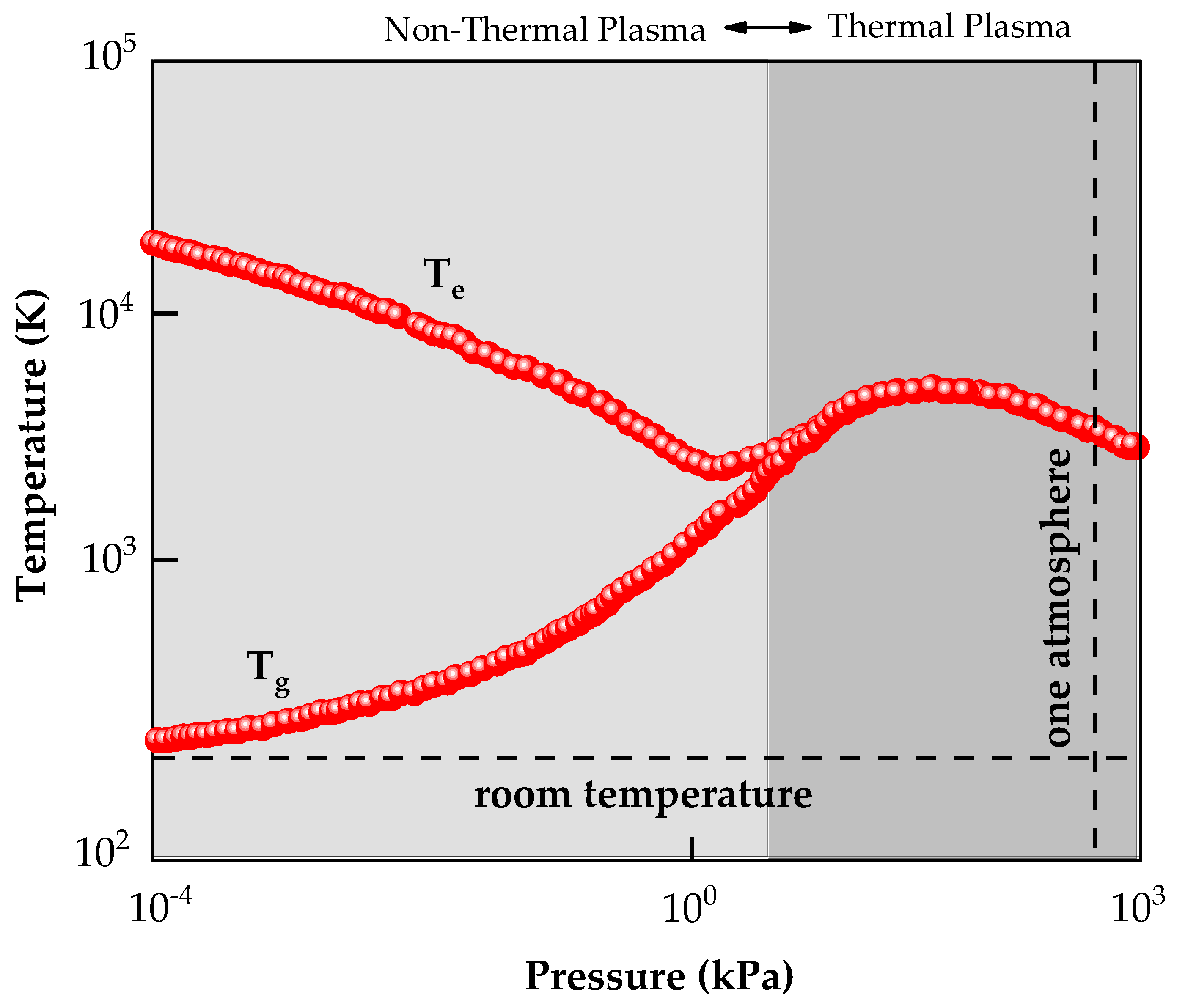
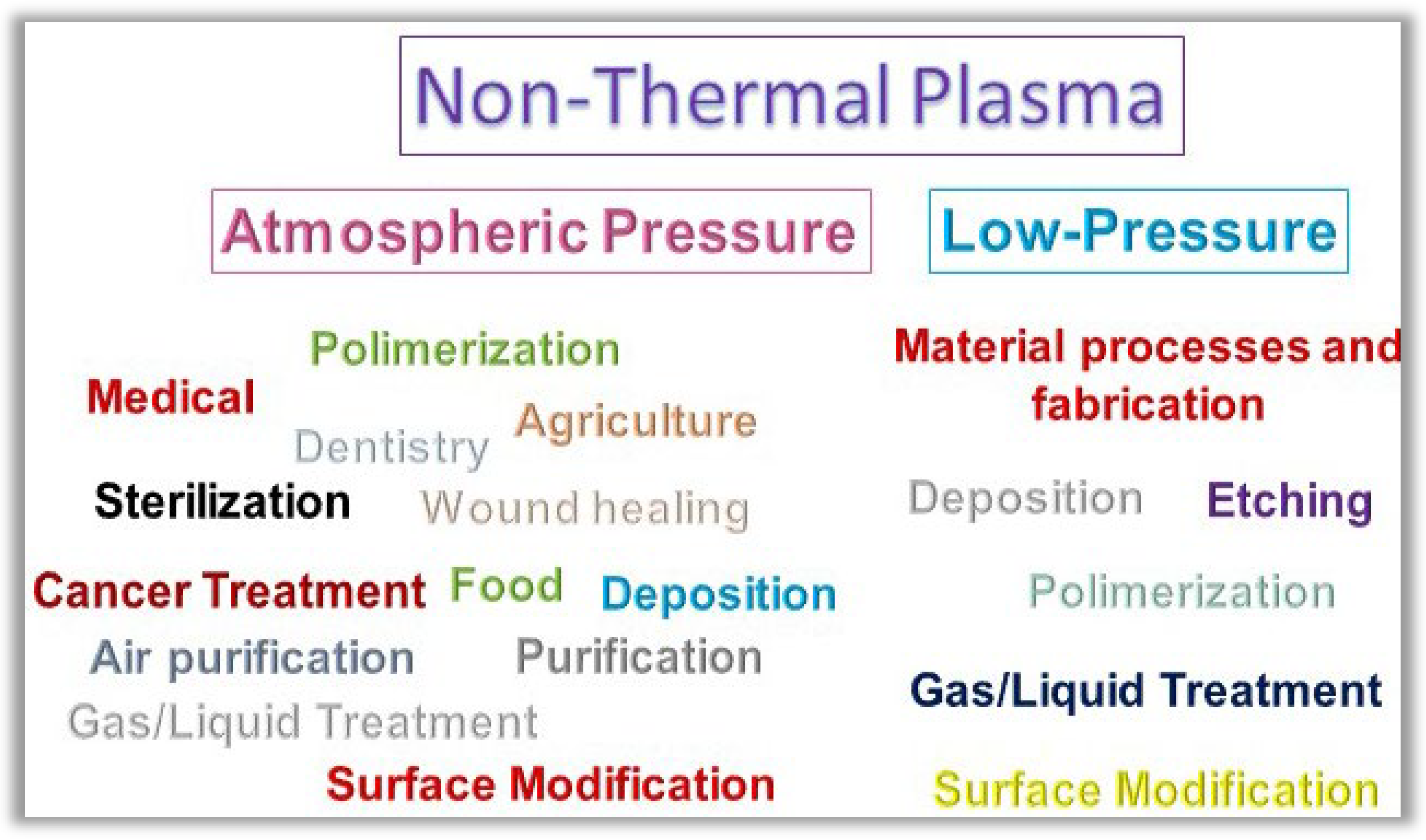
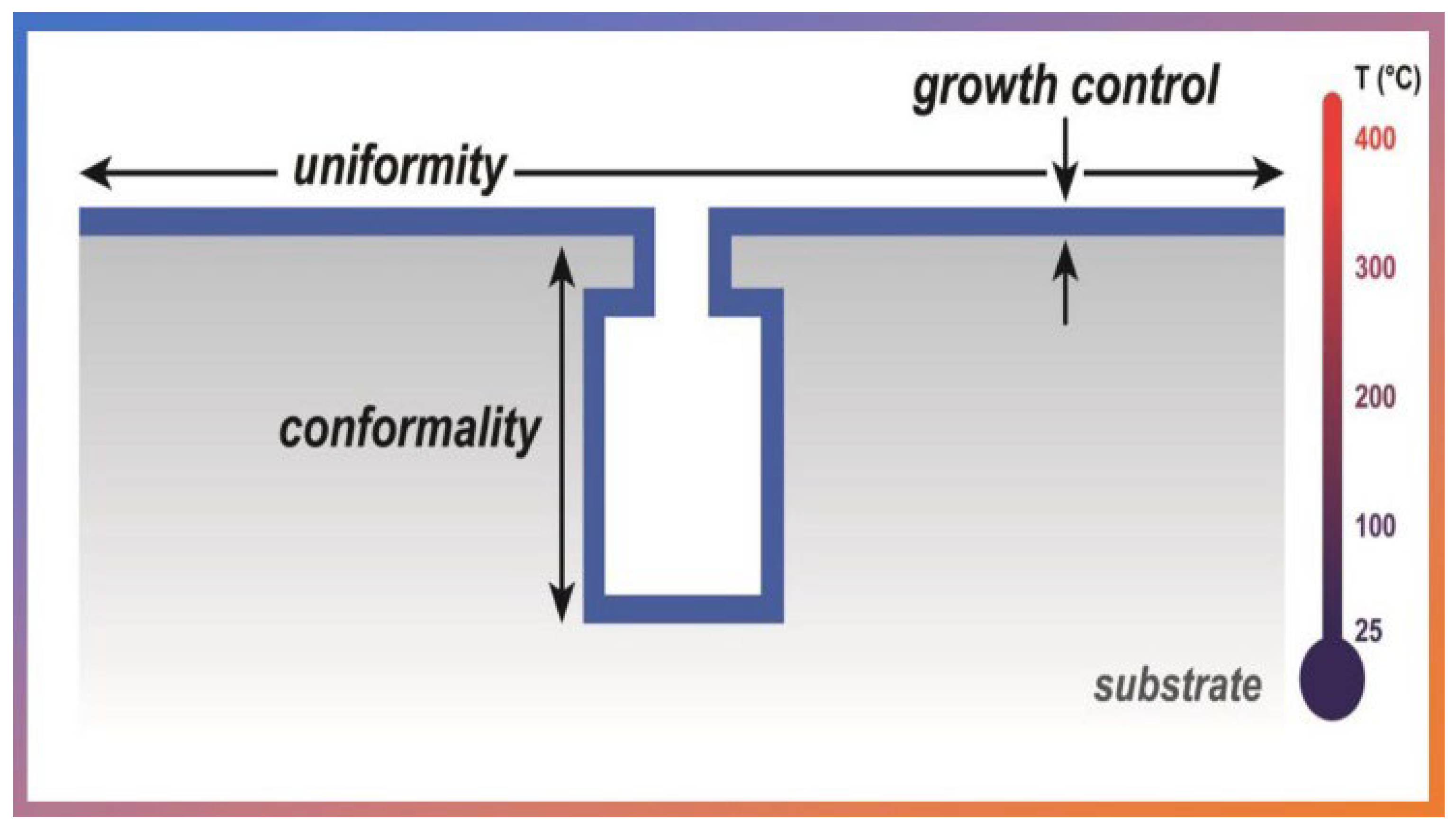
2. Why Non-Thermal Plasma on ALD?
Materials, Plasma Gases and Types of Reactors
3. Main Applications of PA-ALD in Nanofabrication
3.1. Deposition: Plasma-Assisted Atomic Layer Deposition
3.1.1. Oxides
- Wide viewing angle.
- Low latency.
- Low power consumption.
- Ultra-thin lightness and thickness.
- Mechanically flexible.
- (1)
- Yeom et al. [84] grew indium oxide (InOx) using Et2InN(SiMe3)2 and O2 plasma as reactants. The deposition temperature varied between 100 and 250 °C with a GPC of 0.145 nm/cycle. The authors showed that thin-film transistors (TFTs) built with nano-crystalline InOx had a higher carrier density as the temperature ramp increased from 150 to 250 °C. This effect is due to oxygen deficiency at higher deposition temperatures. The TFTs showed high linear mobility of 39.2 cm2 V−1 s−1 for nano-crystalline InOx grown at 250 °C. Therefore, this result indicates that InOx TFTs are a strong candidate for next-generation high-performance TFTs.
- (2)
- Egorov et al. [85] used PA-ALD for TaOx deposition with a controllable concentration of oxygen vacancies (VO). Ta(OC2H5)5 was used as a reactant of Ta, and Ar/H2 plasma as a co-reactant. The VO control made through the fractional mixture of Ar and H2 in the plasma generation was responsible for controlling the leakage current of the resistive switching memory devices in the range of five orders of magnitude compared to the Ta2O5 film grown via thermal ALD. Ultimately they used the Ta2O5/TaOx stack with reliable resistance switching up to approximately 106 switching cycles, in contrast to the single-layer Ta2O5 memory, which demonstrated an order of a few hundred switching cycles.
- (3)
- Jha et al. [86] grew HfO2 thin films by PA-ALD for non-volatile memory applications. For this, they investigated the electrical and ferroelectric properties of metal-insulator-semiconductor (MIS) and metal-insulator-metal (MIM) capacitors with different thicknesses between 5 and 20 nm deposited on Si and TiN/Si. The best results were achieved for 10 nm films. A memory window of 4 V was found for the MIS structure and the MIM structure, with a maximum remaining polarization of 4 μC/cm2. The non-volatile memories based on HfO2 thin films showed a data retention structure of more than ten years with a fatigue resistance of 1012 read/write cycles.
- (4)
- Henning et al. [87] used an aluminum oxide monolayer (~0.3 nm) deposited by PA-ALD for gallium nitride encapsulation in the c-plane (GaN), which is enabled by the partial conversion of surface oxide GaN to AlOx using sequential exposure to trimethylaluminum (TMA) and H2 plasma. This thin AlOx monolayer decreases the work function that increases the reactivity with phosphonic acids under standard conditions, leading to self-assembled monolayers with densities close to the theoretical limit. This high reactivity of TMA with surface oxides opens the opportunity to extend this ultra-fine (<1 nm) aluminum oxide deposition approach to other III-V-based dielectrics and semiconductors, with relevance for applications in (photo) electrocatalysis, optoelectronics, and chemical sensing.
- (5)
- Xiao et al. [88] studied the effect of HfO2 and ZrO2 on n-channel p-channel metal oxide semiconductor field-effect transistors (nFETs and pFETs), CMOS inverters, and CMOS ring oscillators were fabricated to test the quality of HfO2 thin films, and ZrO2 applied as a gate oxide. They used tetrakis(dimethylamino), hafnium (Hf[N(CH3)2]4), and tetrakis (dimethylamino) zirconium (IV) (Zr [N(CH3)2]4) as precursors, respectively, of Hf and Zr. The manufactured nFTTs and pFETs have good electrical properties of n or p-type field-effect transistors, while CMOS inverters based on HfO2 and ZrO2 have good electrical transfer characteristics. Both manufactured ring oscillators demonstrated satisfactory oscillation waveforms, and the ZrO2 gate oxide caused the oscillator to oscillate faster than the HfO2 gate oxide.
3.1.2. Nitrides
3.1.3. Sulfides, Phosphates and Others
3.2. Modification: Surface Modification on Polymers
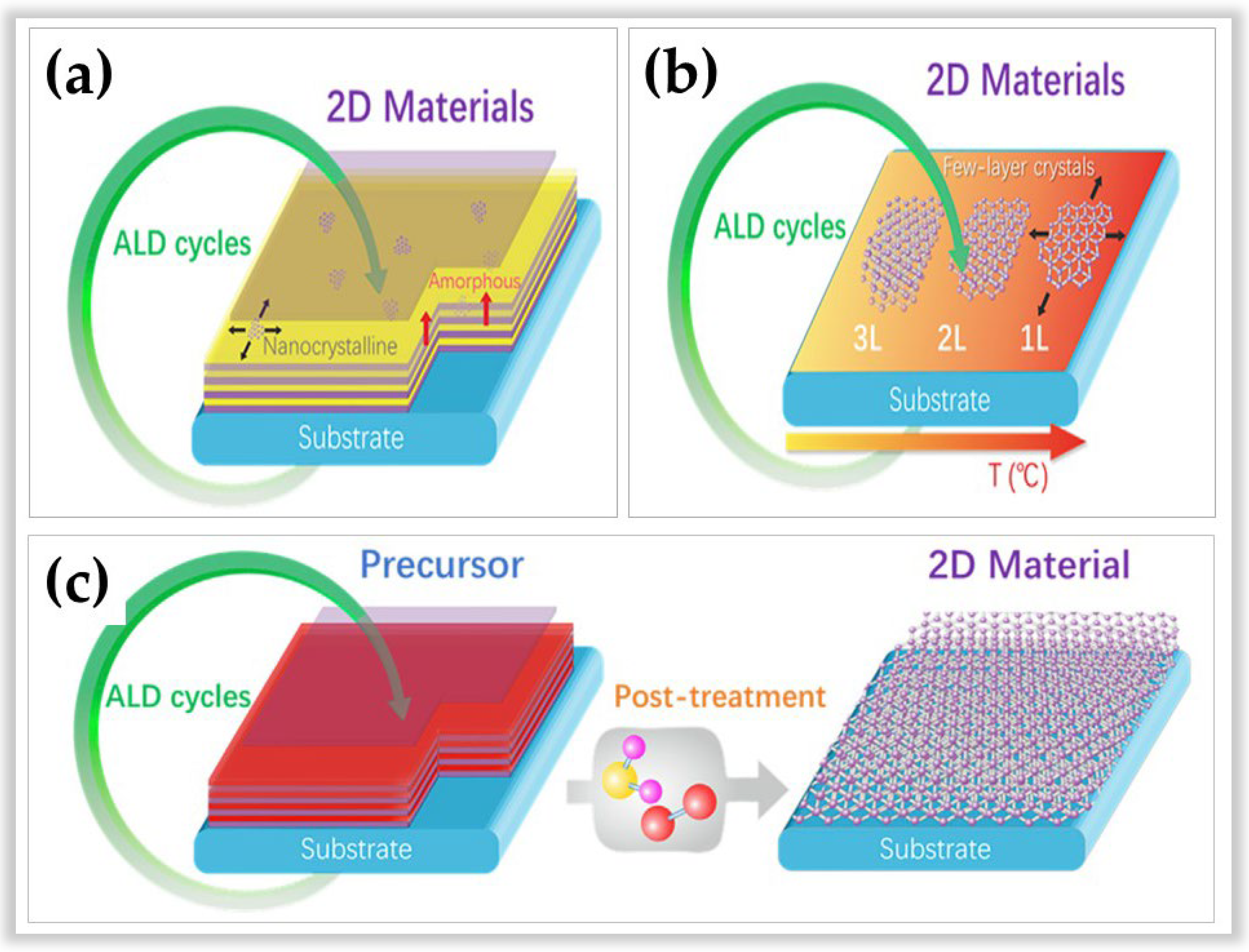
3.3. Efforts to Produce High-Quality 2D Layered Structures
4. Why Non-Thermal Plasma on ALE?
5. Examples of Applications of PA-ALE in Nanofabrication
6. Conclusions
Author Contributions
Funding
Informed Consent Statement
Conflicts of Interest
Appendix A
References
- Langmuir, I. Oscilations in ionized gases. Proc. Natl. Acad. Sci. USA 1928, 14, 627–637. [Google Scholar] [CrossRef] [PubMed] [Green Version]
- Yasuda, H. Plasma for modification of polymers. J. Macromol. Sci. Part A 1976, 10, 383–420. [Google Scholar] [CrossRef]
- Setsuhara, Y. Low-temperature atmospheric-pressure plasma sources for plasma medicine. Arch. Biochem. Biophys. 2016, 605, 3–10. [Google Scholar] [CrossRef] [PubMed]
- Park, J.S.; Han, I.; Choia, E.H. Properties of plasma sterilizer using non-thermal atmospheric-pressure biocompatible plasma. AIP Adv. 2019, 9, 075125. [Google Scholar] [CrossRef] [Green Version]
- López, M.; Calvo, T.; Prieto, M.; Múgica-Vidal, R.; Muro-Fraguas, I.; Alba-Elías, F.; Alvarez-Ordóñez, A. A Review on non-thermal atmospheric plasma for food preservation: Mode of action, determinants of effectiveness, and applications. Front. Microbiol. 2019, 10, 622. [Google Scholar] [CrossRef]
- Waskow, A.; Howling, A.; Furno, I. Mechanisms of plasma-seed treatments as a potential seed processing technology. Front. Phys. 2021, 9, 617345. [Google Scholar] [CrossRef]
- Laurita, R.; Barbieri, D.; Gherardi, M.; Colombo, V.; Lukes, P. Chemical analysis of reactive species and antimicrobial activity of water treated by nanosecond pulsed DBD air plasma. Clin. Plasma Med. 2015, 3, 53–61. [Google Scholar] [CrossRef]
- Cha, S.; Park, Y.-S. Plasma in dentistry. Clin. Plasma Med. 2014, 2, 4–10. [Google Scholar] [CrossRef] [Green Version]
- Doria, A.C.O.C.; Figueira, F.R.; de Lima, J.S.B.; Figueira, J.A.N.; Castro, A.H.R.; Sismanoglu, B.N.; Petraconi, G.; Maciel, H.S.; Khouri, S.; Pessoa, R.S. Inactivation of Candida albicans biofilms by atmospheric gliding arc plasma jet: Effect of gas chemistry/flow and plasma pulsing. Plasma Res. Express 2019, 1, 015001. [Google Scholar] [CrossRef] [Green Version]
- Leite, L.D.P.; Carvalho de Oliveira, A.C.; Vegian, M.R.; Sampaio, A.d.G.; Nishime, T.M.C.; Kostov, K.G.; Koga-Ito, C.Y. Effect of Cold Atmospheric Plasma Jet Associated to Polyene Antifungals on Candida albicans Biofilms. Molecules 2021, 26, 5815. [Google Scholar] [CrossRef]
- Lima, G.M.G.; Borges, A.C.; Nishime, T.M.C.; Santana-Melo, G.F.; Kostov, K.G.; Mayer, M.P.A.; Koga-Ito, C.Y. Cold Atmospheric Plasma Jet as a Possible Adjuvant Therapy for Periodontal Disease. Molecules 2021, 26, 5590. [Google Scholar] [CrossRef] [PubMed]
- Lima, G.M.G.; Carta, C.F.L.; Borges, A.C.; Nishime, T.M.C.; Villela da Silva, C.A.; Caliari, M.V.; Mayer, M.P.A.; Kostov, K.G.; Koga-Ito, C.Y. Cold Atmospheric Pressure Plasma Is Effective against P. gingivalis (HW24D-1) Mature Biofilms and Non-Genotoxic to Oral Cells. Appl. Sci. 2022, 12, 7247. [Google Scholar] [CrossRef]
- Chiappim, W.; Sampaio, A.; Miranda, F.; Fraga, M.; Petraconi, G.; da Silva Sobrinho, A.; Cardoso, P.; Kostov, K.; Koga-Ito, C.; Pessoa, R. Nebulized plasma-activated water has an effective antimicrobial effect on medically relevant microbial species and maintains its physicochemical properties in tube lengths from 0.1 up to 1.0 m. Plasma Processes Polym. 2021, 18, 2100010. [Google Scholar] [CrossRef]
- Chiappim, W.; Sampaio, A.d.G.; Miranda, F.; Fraga, M.; Petraconi, G.; da Silva Sobrinho, A.; Kostov, K.; Koga-Ito, C.; Pessoa, R. Antimicrobial Effect of Plasma-Activated Tap Water on Staphylococcus aureus, Escherichia coli, and Candida albicans. Water 2021, 13, 1480. [Google Scholar] [CrossRef]
- Ouyang, B.; Zhang, Y.; Xia, X.; Rawat, R.S.; Fan, H.J. A brief review on plasma for synthesis and processing of electrode materials. Mater. Today Nano 2018, 3, 28–47. [Google Scholar] [CrossRef]
- Milhan, N.V.M.; Chiappim, W.; Sampaio, A.d.G.; Vegian, M.R.C.; Pessoa, R.S.; Koga-Ito, C.Y. Applications of Plasma-Activated Water in Dentistry: A. Review. Int. J. Mol. Sci. 2022, 23, 4131. [Google Scholar] [CrossRef]
- Schaepkens, M.; Standaert, T.E.F.M.; Rueger, N.R.; Sebel, P.G.M.; Oehrlein, G.S.; Cook, J.M. Study of the SiO2-to-Si3N4 etch selectivity mechanism in inductively coupled fluorocarbon plasmas and a comparison with the SiO2-to-Si mechanism. J. Vac. Sci. Technol. A 1999, 17, 26–37. [Google Scholar] [CrossRef] [Green Version]
- Moreau, M.; Orange, N.; Feuilloley, M.G.J. Non-thermal plasma technologies: New tools for bio-decontamination. Biotechnol. Adv. 2008, 26, 610–617. [Google Scholar] [CrossRef]
- Seo, D.H.; Han, Z.J.; Kumar, S.; Ostrikov, K. Structure-controlled, vertical graphene-based, binder-free electrodes from plasma-reformed butter enhance supercapacitor performance. Adv. Energy Mater. 2013, 3, 1316–1323. [Google Scholar] [CrossRef]
- Azcatl, A.; Qin, X.; Prakash, A.; Zhang, C.; Cheng, L.; Wang, Q.; Lu, N.; Kim, M.J.; Kim, J.; Cho, K.; et al. Covalent nitrogen doping and compressive strain in MoS2 by remote N2 plasma exposure. Nano Lett. 2016, 16, 5437–5443. [Google Scholar] [CrossRef]
- Jozwiak, L.; Balcerzak, J.; Tyczkowski, J. Plasma-deposited Ru-based thin films for photoelectrochemical water splitting. Catalysts 2020, 10, 278. [Google Scholar] [CrossRef] [Green Version]
- Nascimento, L.; Gasi, F.; Landers, R.; da Silva Sobrinho, A.; Aragão, E.; Fraga, M.; Petraconi, G.; Chiappim, W.; Pessoa, R. Physicochemical studies on the surface of polyamide 6.6 fabrics functionalized by DBD plasmas operated at atmospheric and sub-atmospheric pressures. Polymers 2020, 12, 2128. [Google Scholar] [CrossRef] [PubMed]
- Kafle, B.; Ridoy, A.I.; Miethig, E.; Clochard, L.; Duffy, E.; Hofmann, M.; Rentsch, J. On the formation of black silicon features by plasma-less etching of silicon in molecular fluorine gas. Nanomaterials 2020, 10, 2214. [Google Scholar] [CrossRef] [PubMed]
- Fraga, M.; Pessoa, R. Progresses in synthesis and application of SiC films: From CVD to ALD and from MEMS to NEMS. Micromachines 2020, 11, 799. [Google Scholar] [CrossRef]
- Chiappim, W.; Fraga, M.A.; Maciel, H.S.; Pessoa, R.S. An experimental and theoretical study of the impact of the precursor pulse time on the growth per cycle and crystallinity quality of TiO2 thin films grown by ALD and PEALD technique. Front. Mech. Eng. 2020, 6, 551085. [Google Scholar] [CrossRef]
- Puurunen, R.L. Surface chemistry of atomic layer deposition: A case study for the trimethylaluminum/water process. J. Appl. Phys. 2005, 97, 121301. [Google Scholar] [CrossRef]
- Pessoa, R.S.; dos Santos, V.P.; Cardoso, S.B.; Doria, A.C.O.C.; Figueira, F.R.; Rodrigues, B.V.M.; Testoni, G.E.; Fraga, M.A.; Marciano, F.R.; Lobo, A.O.; et al. TiO2 coatings via atomic layer deposition on polyurethane and polydimethylsiloxane substrates: Properties and effects on C. albicans growth and inactivation process. Appl. Surf. Sci. 2017, 422, 73–84. [Google Scholar] [CrossRef]
- Dias, V.; Maciel, H.; Fraga, M.; Lobo, A.O.; Pessoa, R.; Marciano, F.R. Atomic layer deposited TiO2 and Al2O3 thin films as coatings for aluminum food packaging application. Materials 2019, 12, 682. [Google Scholar] [CrossRef] [Green Version]
- Dias, V.M.; Chiappim, W.; Fraga, M.A.; Maciel, H.S.; Marciano, F.R.; Pessoa, R.S. Atomic layer deposition of TiO2 and Al2O3 thin films for the electrochemical study of corrosion protection in aluminum alloy cans used in beverage. Mater. Res. Express 2020, 7, 076408. [Google Scholar] [CrossRef]
- Khan, M.R.; Kim, H.G.; Park, J.S.; Shin, J.W.; Nguyen, C.T.; Lee, H.-B.-R. Tunable color coating of e-textiles by atomic layer deposition of multilayer TiO2/Al2O3 films. Langmuir 2020, 36, 2794–2801. [Google Scholar] [CrossRef]
- Curado, M.A.; Teixeira, J.P.; Monteiro, M.; Ribeiro, E.F.M.; Vilão, R.C.; Alberto, H.V.; Cunha, J.M.V.; Lopes, T.S.; Oliveira, K.; Donzel-Gargand, O.; et al. Front passivation of Cu(In,Ga)Se2 solar cells using Al2O3: Culprits and benefits. Appl. Mater. Today 2020, 21, 100867. [Google Scholar] [CrossRef]
- Chiappim Júnior, W.; Moreno, L.X.; Pessoa, R.S.; da Cunha, A.F.; Salomé, P.M.P.; Leitão, J.P. Novel Dielectrics Compounds Grown by Atomic Layer Deposition as Sustainable Materials for Chalcogenides Thin Films Photovoltaics Technologies. In Sustainable Materials Solutions for Solar Energy Technologies: Processing Techniques and Applications, 1st ed.; Fraga, M.A., Amos, D., Sonmezoglu, S., Subramaniam, V., Eds.; Elsevier: Amsterdam, The Netherlands, 2021; Volume 1, pp. 71–100. [Google Scholar]
- Pessoa, R.S.; Chiappim Júnior, W.; Fraga, M.A. Atomic Layer Deposition of Materials for Solar Water Splitting. In Sustainable Materials Solutions for Solar Energy Technologies: Processing Techniques and Applications, 1st ed.; Fraga, M.A., Amos, D., Sonmezoglu, S., Subramaniam, V., Eds.; Elsevier: Amsterdam, The Netherlands, 2021; Volume 1, pp. 363–380. [Google Scholar]
- Pessoa, R.S.; Fraga, M.A.; Chiappim, W.; Maciel, H.S. Exploring the Properties and Fuel Cell Applications of Ultrathin Atomic Layer Deposited Metal Oxide Films. In Emerging Materials for Energy Conversion and Storage, 1st ed.; Cheong, K.Y., Impellizzeri, G., Fraga, M.A., Eds.; Elsevier: Amsterdam, The Netherlands, 2018; Volume 1, pp. 83–114. [Google Scholar]
- Mattinen, M.; Popov, G.; Vehkamäki, M.; King, P.J.; Mizohata, K.; Jalkanen, P.; Räisänen, J.; Leskelä, M.; Ritala, M. Atomic layer deposition of emerging 2D semiconductors, HfS2 and ZrS2, for optoelectronics. Chem. Mater. 2019, 31, 5713–5724. [Google Scholar] [CrossRef] [Green Version]
- Weber, M.; Julbe, A.; Ayral, A.; Miele, P.; Bechelany, M. Atomic layer deposition for membranes: Basics, challenges, and opportunities. Chem. Mater. 2018, 30, 7368–7390. [Google Scholar] [CrossRef]
- Weber, M.; Julbe, A.; Kim, S.S.; Bechelany, M. Atomic layer deposition (ALD) on inorganic or polymeric membranes. J. Appl. Phys. 2019, 126, 041101. [Google Scholar] [CrossRef]
- Astaneh, S.H.; Faverani, L.P.; Sukotjo, C.; Takoudis, C.G. Atomic layer deposition on dental materials: Processing conditions and surface functionalization to improve physical, chemical, and clinical properties—A review. Acta Biomater. 2021, 121, 103–118. [Google Scholar] [CrossRef]
- La Zara, D.; Zhang, F.; Sun, F.; Bailey, M.R.; Quayle, M.J.; Petersson, G.; Folestad, S.; van Ommen, J.R. Drug powders with tunable wettability by atomic and molecular layer deposition: From highly hydrophilic to superhydrophobic. Appl. Mater. Today 2021, 22, 100945. [Google Scholar] [CrossRef]
- Botas, A.M.P.; Leitão, J.P.; Falcão, B.P.; Wiesinger, M.; Eckmann, F.; Teixeira, J.P.; Wiggers, H.; Stutzmann, M.; Ferreira, R.A.S.; Pereira, R.N. Silicon nanoparticles films infilled with Al2O3 using atomic layer deposition for photosensor, light emission, and photovoltaic applications. ACS Appl. Nano Mater. 2020, 3, 5033–5044. [Google Scholar] [CrossRef]
- Mackus, A.J.M.; Merkx, M.J.M.; Li, J. Area-selective atomic layer deposition for bottom-up fabrication of nanoelectronics. Nevac Blad 2020, 58, 32–34. [Google Scholar]
- Seweryn, A.; Lawniczak-Jablonska, K.; Kuzmiuk, P.; Gieraltowska, S.; Godlewski, M.; Mroczynski, R. Investigations of structural and electrical properties of ALD films formed with the ozone precursor. Materials 2021, 14, 5395. [Google Scholar] [CrossRef]
- Kim, S.H.; Song, S.Y.; Kim, S.Y.; Chang, M.W.; Kwon, H.J.; Yoon, K.H.; Sung, W.Y.; Sung, M.M.; Chu, H.Y. A compact polymer–inorganic hybrid gas barrier nanolayer for flexible organic light-emitting diode displays. NPJ Flex. Electron. 2022, 10, 1849. [Google Scholar] [CrossRef]
- Petit, R.R.; Li, J.; Van de Voorde, B.; Van Vlierberghe, S.; Smet, P.F.; Detavernier, C. Atomic Layer Deposition on Polymer Thin Films: On the Role of Precursor Infiltration and Reactivity. ACS Appl. Mater. Interfaces 2021, 13, 46151–46163. [Google Scholar] [CrossRef] [PubMed]
- Kanarik, K.J.; Lill, T.; Hudson, E.A.; Sriraman, S.; Tan, S.; Marks, J.; Vahedi, V.; Gottscho, R.A. Overview of atomic layer etching in the semiconductor industry. J. Vac. Sci. Technol. A 2015, 33, 020802. [Google Scholar] [CrossRef] [Green Version]
- Kanarik, K.J.; Tan, S.; Gottscho, R.A. Atomic Layer Etching: Rethinking the Art of Etch. J. Phys. Chem. Lett. 2018, 9, 4814–4821. [Google Scholar] [CrossRef] [PubMed] [Green Version]
- Knoops, H.C.M.; Potts, S.E.; Bol, A.A.; Kessels, W.M.M. Atomic Layer Deposition. In Handbook of Crystal Growth, 2nd ed.; Kuech, T.F., Ed.; Elsevier: Amsterdam, The Netherlands, 2015; Volume 1, pp. 1101–1134. [Google Scholar]
- Profijt, H.B.; Potts, S.E.; van de Sanden, M.C.M.; Kessels, W.M.M. Plasma-assisted atomic layer deposition: Basics, opportunities, and challenges. J. Vac. Sci. Technol. A 2011, 29, 050801. [Google Scholar] [CrossRef] [Green Version]
- Johnson, R.W.; Hultqvist, A.; Bent, S.F. A brief review of atomic layer deposition: From fundamentals to applications. Mater. Today 2014, 17, 236–246. [Google Scholar] [CrossRef]
- Knoops, H.C.M.; Faraz, T.; Arts, K.; Kessels, W.M.M. Status and prospects of plasma-assisted atomic layer deposition. J. Vac. Sci. Technol. A 2019, 23, 030902. [Google Scholar] [CrossRef] [Green Version]
- De Keijser, M.; van Opdorp, C. Atomic layer epitaxy of gallium arsenide with the use of atomic hydrogen. Appl. Phys. Lett. 1991, 58, 1187. [Google Scholar] [CrossRef]
- Rossnagel, S.M.; Sherman, A.; Turner, F. Plasma-enhanced atomic layer deposition of Ta and Ti for interconnect diffusion barriers. J. Vac. Sci. Technol. A 2000, 18, 2016. [Google Scholar] [CrossRef]
- Ratzsch, S.; Kley, E.-B.; Tünnermann, A.; Szeghalmi, A. Influence of the oxygen plasma parameters on the atomic layer deposition of titanium dioxide. Nanotechnology 2015, 26, 024003. [Google Scholar] [CrossRef]
- Chiappim, W.; Testoni, G.E.; Doria, A.C.O.C.; Pessoa, R.S.; Fraga, M.A.; Galvão, N.K.A.M.; Grigorov, K.G.; Vieira, L.; Maciel, H.S. Relationships among growth mechanism, structure and morphology of PEALD TiO2 films: The influence of O2 plasma power, precursor chemistry and plasma exposure mode. Nanotechnology 2016, 27, 305701. [Google Scholar] [CrossRef]
- Chiappim, W.; Watanabe, M.; Dias, V.; Testoni, G.; Rangel, R.; Fraga, M.; Maciel, H.; dos Santos Filho, S.; Pessoa, R. MOS cpacitance measurements for PEALD TiO2 dielectrics films grown under different conditions and the impact of Al2O3 partial-monolayer inserction. Nanomaterials 2020, 10, 338. [Google Scholar] [CrossRef]
- Belahcen, S.; Vallée, C.; Bsiesy, A.; Chaker, A.; Jaffal, M.; Yeghoyan, T.; Bonvalot, M. Control of ion energy during plasma enhanced atomic layer deposition: A new strategy for the modulation of TiN growth delay on SiO2. J. Vac. Sci. Technol. A 2020, 39, 012410. [Google Scholar] [CrossRef]
- Potts, S.E.; Keuning, W.; Langereis, E.; Dingemans, G.; van de Sanden, M.C.M.; Kessels, W.M.M. Low temperature plasma-enhanced atomic layer deposition of metal oxide thin films. J. Electrochem. Soc. 2010, 157, P66–P74. [Google Scholar] [CrossRef]
- Chiappim, W.; Testoni, G.; Miranda, F.; Fraga, M.; Furlan, H.; Saravia, D.A.; da Silva Sobrinho, A.; Petraconi, G.; Maciel, H.; Pessoa, R. Effect of plasma-enhanced atomic layer deposition on oxygen overabundance and its influence on the morphological, optical, structural, and mechanical properties of Al-doped TiO2 coating. Micromachines 2021, 12, 588. [Google Scholar] [CrossRef]
- Seppänen, H.; Kim, I.; Etula, J.; Ubyivovk, E.; Bouravleuv, A.; Lipsanen, H. Aluminum nitride transition layer for power electronics applications grown by plasma-enhanced atomic layer deposition. Materials 2019, 12, 406. [Google Scholar] [CrossRef] [Green Version]
- Kuhs, J.; Dobbelaere, T.; Hens, Z. Plasma enhanced atomic layer deposition of zinc sulfide thin films. J. Vac. Sci. Technol. A 2017, 35, 01B111. [Google Scholar] [CrossRef] [Green Version]
- Vos, M.F.J.; Knoops, H.C.M.; Synowicki, R.A.; Kessels, W.M.M.; Mackus, A.J.M. Atomic layer depositions of aluminum fluoride using Al(CH3)3 and SF6 plasma. Appl. Phys. Lett. 2017, 111, 113105. [Google Scholar] [CrossRef]
- Dobbelaere, T.; Mattelaer, F.; Vereecken, P.M.; Detavernier, C. Plasma-enhanced atomic layer deposition of vanadium phosphate as a lithium-ion battery electrode material. J. Vac. Sci. Technol. A 2017, 35, 041513. [Google Scholar] [CrossRef] [Green Version]
- Griffiths, M.B.E.; Pallister, P.J.; Mandia, D.J.; Barry, S.T. Atomic layer deposition of gold metal. Chem. Mater. 2016, 28, 44–46. [Google Scholar] [CrossRef]
- Tvarog, D.; Olejnícek, J.; Kratochvíl, J.; Ksírova, P.; Poruba, A.; Hubicka, Z.; Cada, M. Characterization of radical-enhanced atomic layer deposition process based on microwave surface generated plasma. J. Appl. Phys. 2021, 130, 013301. [Google Scholar] [CrossRef]
- Ozgit-Akgun, C.; Goldenberg, E.; Okyay, A.K.; Biyikli, N. Hollow cathode plasma-assisted atomic layer deposition of crystalline AlN, GaN and AlxGa1-xN thin films at low temperatures. J. Mater. Chem. C 2014, 2, 2123–2136. [Google Scholar] [CrossRef]
- Xiong, Y.-Q.; Li, X.-C.; Chen, Q.; Lei, W.-W.; Zhao, Q.; Sang, L.-J.; Liu, Z.-W.; Wang, Z.-D.; Yang, L.-Z. Characteristics and properties of metal aluminum thin films prepared by electron cyclotron resonance plasma-assisted atomic layer deposition technology. Chin. Phys. B 2012, 21, 078105. [Google Scholar] [CrossRef]
- Starostin, S.A.; Keuning, W.; Schalken, J.-P.; Creatore, M.; Kessels, W.M.M.; Bouwstra, J.B.; van de Sanden, C.M.; de Vries, H.W. Synergy between plasma-assisted ALD and roll-to-roll atmospheric pressure PE-CVD processing of moisture barrier films on polymers. Plasma Process. Polym. 2015, 13, 311–315. [Google Scholar] [CrossRef] [Green Version]
- Ziegler, J.; Mews, M.; Kaufmann, K.; Schneider, T.; Sprafke, A.N.; Korte, L.; Wehrspohn, R.B. Plasma-enhanced atomic-layer-deposited MoOx emitters for silicon heterojunction solar cells. Appl. Phys. A 2015, 120, 811–816. [Google Scholar] [CrossRef] [Green Version]
- Garud, S.; Gampa, N.; Allen, T.G.; Kotipalli, R.; Flandre, D.; Batuk, M.; Hadermann, J.; Meuris, M.; Poortmans, J.; Smets, A.; et al. Surface passivation of CIGS solar cells using gallium oxide. Phys. Status Solidi A 2018, 215, 1700826. [Google Scholar] [CrossRef] [Green Version]
- Ghods, A.; Saravade, V.G.; Zhou, C.; Ferguson, I.T. Field-effect passivation of metal/n-GaAs Schottky junction solar cells using atomic layer deposited Al2O3/ZnO ultrathin films. J. Vac. Sci. Technol. A 2020, 38, 012406. [Google Scholar] [CrossRef]
- Koushik, D.; Jost, M.; Ducinskas, A.; Burgess, C.; Zardetto, V.; Weijtens, C.; Verheijen, M.A.; Kessels, W.M.M.; Albrecht, S.; Creatore, M. Plasma-assisted atomic layer deposition of nickel oxide as hole transport layer for hybrid perovskite solar cells. J. Mater. Chem. C 2019, 7, 12532–12543. [Google Scholar] [CrossRef] [Green Version]
- Imai, T.; Mori, Y.; Kanomata, K.; Miura, M.; Ahmmad, B.; Kubota, S.; Hirose, F. Room-temperature plasma enhanced atomic layer deposition of aluminum silicate and its application in dye-sensitized solar cells. J. Vac. Sci. Technol. A 2018, 36, 01A106. [Google Scholar] [CrossRef]
- Potscavage, W.J.; Yoo, S.; Domercq, B.; Kippelen, B. Encapsulation of pentacene/C60 organic solar cells with Al2O3 deposited by atomic layer deposition. Appl. Phys. Lett. 2007, 90, 253511. [Google Scholar] [CrossRef] [Green Version]
- Wei, H.; Qiu, P.; Peng, M.; Wu, Q.; Liu, S.; Na, Y.; He, Y.; Song, Y.; Zheng, X. Interface modification for high-efficient quantum dot sensitized solar cells using ultrathin aluminum nitride coating. Appl. Surf. Sci. 2019, 476, 608–614. [Google Scholar] [CrossRef]
- Wang, C.; Zhao, D.; Grice, C.R.; Liao, W.; Yu, Y.; Cimaroli, A.; Shrestha, N.; Roland, P.J.; Chen, J.; Yu, Z.; et al. Low-temperature plasma-enhanced atomic layer deposition of tin oxide electron selective layers for highly efficient planar perovskite solar cells. J. Mater. Chem. A 2016, 4, 12080–12087. [Google Scholar] [CrossRef]
- Reichel, C.; Reusch, M.; Kotula, S.; Granek, F.; Richter, A.; Hermle, M.; Glunz, S.W. Insulating and passivating plasma-enhanced atomic layer deposited aluminum oxide thin films for silicon solar cells. Thin Solid Films 2018, 656, 53–60. [Google Scholar] [CrossRef]
- Wang, H.; Zhao, Y.; Wang, Z.; Liu, Y.; Zhao, Z.; Xu, G.; Han, T.-H.; Lee, J.-W.; Chen, C.; Bao, D.; et al. Hermetic seal for perovskite solar cells: An improved plasma enhanced atomic layer deposition encapsulation. Nano Energy 2020, 69, 104375. [Google Scholar] [CrossRef]
- Wang, D.; Wright, M.; Elumalai, N.K.; Uddin, A. Stability of perovskite solar cells. Sol. Energy Mater. Sol. Cells 2016, 147, 255–275. [Google Scholar] [CrossRef]
- Han, T.-H.; Lee, Y.; Choi, M.-R.; Woo, S.-H.; Bae, S.-H.; Hong, B.H.; Ahn, J.-H.; Lee, T.-W. Extremely efficient flexible organic light-emitting diodes with modified graphene anode. Nat. Photonics 2012, 6, 105–110. [Google Scholar] [CrossRef]
- Aziz, H.; Popovic, Z.; Xie, S.; Hor, A.-M.; Hu, N.-X.; Tripp, C.; Xu, G. Humidity-induced crystallization of tris(8-hydroxyquinoline) aluminum layers in organic light-emitting devices. Appl. Phys. Lett. 1998, 72, 756. [Google Scholar] [CrossRef]
- Hoffmann, L.; Theirich, D.; Hasselman, T.; Räupke, A.; Schlaman, D.; Riedl, T. Gas permeation barriers deposited by atmospheric pressure plasma enhanced atomic layer deposition. J. Vac. Sci. Technol. A 2016, 34, 01A114. [Google Scholar] [CrossRef]
- Kim, L.H.; Jeong, Y.J.; An, T.K.; Park, S.; Jang, J.H.; Nam, S.; Jang, J.; Kim, S.H.; Park, C.E. Optimization of Al2O3/TiO2 nanolaminates thin films prepared with different oxide ratios, for use in organic light-emitting diode encapsulation, via plasma-enhanced atomic layer deposition. Phys. Chem. Chem. Phys. 2016, 18, 1042. [Google Scholar] [CrossRef]
- Jing, Y.; Merkx, J.M.; Cai, J.; Cao, K.; Kessels, W.M.M.; Mackus, J.M.; Chen, R. Nanoscale encapsulation of perovskite nanocrystal luminescent films via plasma-enhanced SiO2 atomic layer deposition. ACS Appl. Mater. Interfaces 2020, 12, 53519–53527. [Google Scholar] [CrossRef]
- Yeom, H.-I.; Ko, J.B.; Mun, G.; Park, S.-H.K. High mobility polycrystalline indium oxide thin-film transistors by means of plasma-enhanced atomic layer deposition. J. Mater. Chem. C 2016, 4, 6873–6880. [Google Scholar] [CrossRef] [Green Version]
- Egorov, K.V.; Kuzmichev, D.S.; Chizhov, P.S.; Lebedinskii, Y.Y.; Hwang, C.S.; Markeev, A.M. In situ control of oxygen vacancies in TaOx thin films via plasma-enhanced atomic layer deposition for resistive switching memory applications. ACS Appl. Mater. Interfaces 2017, 9, 13286–13292. [Google Scholar] [CrossRef] [PubMed]
- Jha, R.K.; Singh, P.; Goswami, M.; Singh, B.R. Plasma enhanced atomic layer deposition HfO2 ferroelectric films for non-volatile memory applications. J. Electron. Mater. 2020, 49, 1445–1453. [Google Scholar] [CrossRef]
- Henning, A.; Bartl, J.D.; Zeidler, A.; Qian, S.; Bienek, O.; Jiang, C.-M.; Paulus, C.; Rieger, B.; Stutzmann, M.; Sharp, I.D. Aluminum oxide at the monolayer limit via oxidant-free plasma-assisted atomic layer deposition on GaN. Adv. Funct. Mater. 2021, 31, 2101441. [Google Scholar] [CrossRef]
- Xiao, Z.; Kisslinger, K.; Chance, S.; Banks, S. Comparison of hafnium dioxide and zirconium dioxide by plasma-enhanced atomic layer deposition for the application of electronic materials. Crystals 2020, 10, 136. [Google Scholar] [CrossRef] [Green Version]
- Otto, L.M.; Hammack, A.T.; Aloni, S.; Ogletree, D.F.; Olynick, L.; Dhuey, S.; Stadler, J.H.; Schwartzberg, A.M. Plasma-enhanced atomic layer deposition for plasmonic TiN. Proc. SPIE 2016, 9919, 99190N. [Google Scholar]
- Krylov, I.; Zoubenko, E.; Weinfeld, K.; Kauffman, Y.; Xu, X.; Ritter, D.; Eizenberg, M. Obtaining low resitivity (~100 uW cm) TiN films by plasma enhanced atomic layer deposition using a metalorganic precursor. J. Vac. Sci. Technol. 2018, 36, 051505. [Google Scholar] [CrossRef]
- Kim, H.; Song, H.; Shin, C.; Kim, K.; Jang, W.; Kim, H.; Shin, S.; Jeon, H. Dielectric barrier characteristics of Si-rich silicon nitride films deposited by plasma atomic layer deposition. J. Vac. Sci. Technol. 2017, 35, 01A101-1. [Google Scholar] [CrossRef]
- Han, J.H.; Kim, H.Y.; Lee, S.C.; Kim, D.H.; Park, B.K.; Park, J.-S.; Jeon, D.J.; Chung, T.-M.; Kim, C.G. Growth of tantalum nitride film as a Cu diffusion barrier by plasma-enhanced atomic layer deposition from bis((2-(dimethylamino)ethyl)(methyl)amido)methyl(tert-butylimido)tantalum complex. Appl. Surf. Sci. 2016, 362, 176–181. [Google Scholar] [CrossRef]
- Wang, X.-Z.; Muneshwar, T.P.; Fan, H.-Q.; Cadien, K.; Luo, J.-L. Achieving ultrahigh corrosion resistance and conductive zirconium oxynitride coating on metal bipolar plates by plasma enhanced atomic layer deposition. J. Power Sources 2018, 397, 32–36. [Google Scholar] [CrossRef]
- Sowa, M.J.; Yemane, Y.; Zhang, J.; Palmstrom, J.C.; Ju, L.; Strandwitz, N.C.; Prinz, F.B.; Provine, J. Plasma-enhanced atomic layer deposition of superconducting niobium nitride. J. Vac. Sci. Technol. A 2017, 35, 01B143. [Google Scholar] [CrossRef]
- Tian, L.; Bottala-Gambetta, I.; Marchetto, V.; Jacquemin, M.; Crisci, A.; Reboud, R.; Mantoux, A.; Berthomé, G.; Mercier, F.; Sulpice, A.; et al. Improved critical temperature of superconducting plasma-enhanced atomic layer deposition of niobium nitride thin films by thermal annealing. Thin Solid Films 2020, 709, 138232. [Google Scholar] [CrossRef]
- Di Bartolomeo, A. Emerging 2D materials and their Van der Waals heterostructures. Nanomaterials 2020, 10, 579. [Google Scholar] [CrossRef]
- Groven, B.; Heyne, M.; Mehta, A.N.; Bender, H.; Nuytten, T.; Meersschaut, J.; Conard, T.; Verdock, P.; Elshocht, S.V.; Vandervorst, W.; et al. Plasma-enhanced atomic layer deposition of two-dimensional WS2 from WF6, H2 plasma, and H2S. Chem. Mater. 2017, 29, 2927–2938. [Google Scholar] [CrossRef]
- Balasubramanyam, S.; Shirazi, M.; Bloodgood, M.A.; Wu, L.; Verheijen, M.A.; Vandalon, V.; Kessels, W.M.M.; Hofmann, J.P.; Bol, A.A. Edge-site nanoengineering of WS2 by low-temperature plasma-enhanced atomic layer deposition for electrocatalytic hydrogen evolution. Chem. Mater. 2019, 31, 5104–5115. [Google Scholar] [CrossRef] [Green Version]
- Sharma, A.; Verheijen, A.; Wu, L.; Karwal, S.; Vandalon, V.; Knoops, H.C.M.; Sundaram, R.S.; Hofmann, J.P.; Kessels, W.M.M.; Bol, A.A. Low-temperature plasma-enhanced atomic layer deposition of 2D MoS2: Large area, thickness control and tunable morphology. Nanoscale 2018, 10, 8615–8627. [Google Scholar] [CrossRef]
- Vandalon, V.; Verheijen, M.A.; Kessels, W.M.M.; Bol, A.A. Atomic layer deposition of Al doped MoS: Synthesizing a p-type 2D semiconductor with tunable carrier density. ACS Appl. Nano Mater. 2020, 3, 10200–10208. [Google Scholar] [CrossRef]
- Bugot, C.; Bouttemy, M.; Schneider, N.; Etcheberry, A.; Lincot, D.; Donsanti, F. New insights on the chemistry of plasma-enhanced atomic layer deposition of indium oxysulfide thin films and their use as buffer layers in Cu(In,Ga)Se2 thin film solar cell. J. Vac. Sci. Technol. 2018, 36, 061510. [Google Scholar] [CrossRef]
- Wang, H.; Song, S.; Song, Z.; Zhou, Z.; Yao, D.; Lv, S. Fast and scalable phase change materials Ti-Sb-Te deposited by plasma-enhanced atomic layer deposition. J. Mater. Sci. Mater. Electron. 2020, 31, 5833–5837. [Google Scholar] [CrossRef]
- Giordano, M.C.; Baumgaertl, K.; Steinvall, S.E.; Vuichard, M.; Fontcuberta i Morral, A.; Grundler, D. Plasma-enhanced atomic layer deposition of nickel nanotubes with low resistivity and coherent magnetization dynamics for 3D spintronics. ACS Appl. Mater. Interfaces 2020, 12, 40443–40452. [Google Scholar] [CrossRef]
- Chiper, A.S. Tailoring the working gas flow to improve the surface modification of plasma-treated polymer. Mat. Lett. 2021, 305, 130832. [Google Scholar] [CrossRef]
- Levchenko, I.; Xu, S.; Baranov, O.; Bazaka, O.; Ivanova, E.P.; Bazaka, K. Plasma and Polymers: Recent progress and trends. Molecules 2021, 26, 4091. [Google Scholar] [CrossRef]
- Parsons, G.N.; Atasanov, S.E.; Dandley, E.C.; Devine, C.K.; Gong, B.; Jur, J.S.; Lee, K.; Oldham, C.J.; Peng, Q.; Spagnola, J.C.; et al. Mechanism and reactions during atomic layer deposition on polymers. Coord. Chem. Rev. 2013, 257, 3323–3331. [Google Scholar] [CrossRef]
- Kim, G.H.; Lee, J.G.; Kim, S.S. Surface modification of polymeric substrates to enhance the barrier properties of an Al2O3 layer formed by PEALD. Org. Electron. 2017, 50, 239–246. [Google Scholar] [CrossRef]
- Kääriäinen, T.O.; Lehti, S.; Kääriäinen, M.-L.; Cameron, D.C. Surface modification of polymers by plasma-assisted atomic layer deposition. Surf. Coat. Technol. 2011, 205, S475–S479. [Google Scholar] [CrossRef]
- Cho, S.-W.; Jeong, J.-A.; Bae, J.-H.; Moon, J.-M.; Choi, K.-H.; Jeong, S.W.; Park, N.-J.; Kim, J.-J.; Lee, S.H.; Kang, J.-W.; et al. Highly flexible, transparent, and low resistance indium zinc oxide-Ag-indium zinc oxide multilayer anode on polyethylene terephthalate substrate for flexible organic light light-emitting diodes. Thin Solid Films 2008, 516, 7881–7885. [Google Scholar] [CrossRef]
- Rahy, A.; Bajaj, P.; Musselman, I.H.; Hong, S.H.; Sun, Y.-P.; Yang, D.J. Coating of carbon nanotubes on flexible substrate and its adhesion study. Appl. Surf. Sci. 2009, 255, 7084–7089. [Google Scholar] [CrossRef]
- Choi, M.-C.; Kim, Y.; Ha, C.-S. Polymers for flexible displays: From material selection to device applications. Prog. Polym. Sci. 2008, 33, 581–630. [Google Scholar] [CrossRef]
- Fang, M.; Zhang, H.; Sang, L.; Cao, H.; Yang, L.; Ostrikov, K.; Levchenko, I.; Chen, Q. Plasma-assisted ALD to functionalize PET: Towards new generation flexible gadgets. Flex. Print. Electron. 2017, 2, 022001. [Google Scholar] [CrossRef]
- Lee, Y.; Seo, S.; Oh, I.-K.; Lee, S.; Kim, H. Effects of O2 plasma treatment on moisture barrier properties of SiO2 grown by plasma-enhanced atomic layer deposition. Ceram. Int. 2019, 45, 17662–17668. [Google Scholar] [CrossRef]
- Kovács, R.L.; Gyöngyösi, S.; Langer, G.; Baradács, E.; Daróczi, L.; Barkóczy, P.; Erdélyi, Z. Effect of nanoscopic defects on barrier performance of thin films deposited by plasma-enhanced atomic layer deposition on flexible polymers. Thin Solid Films 2021, 738, 138960. [Google Scholar] [CrossRef]
- Sun, C.; Zhang, J.; Zhang, Y.; Zhao, F.; Xie, J.; Liu, Z.; Zhuang, J.; Zhang, N.; Ren, W.; Ye, Z.-G. Design and fabrication of flexible strain sensor based on ZnO-decorated PVDF via atomic layer deposition. Appl. Surf. Sci. 2021, 562, 150126. [Google Scholar] [CrossRef]
- Cai, J.; Han, X.; Wang, X.; Meng, X. Atomic Layer Deposition of Two-Dimensional Layered Materials: Processes, Growth Mechanisms, and Characteristics. Matter 2020, 2, 587–630. [Google Scholar] [CrossRef]
- Haider, A.; Ozgit-Akgun, C.; Goldenberg, E.; Okyay, A.K.; Biyikli, N. Low-Temperature Deposition of Hexagonal Boron Nitride via Sequential Injection of Triethylboron and N2/H2 Plasma. J. Am. Ceram. 2014, 97, 4052–4059. [Google Scholar] [CrossRef] [Green Version]
- Park, H.; Kim, T.K.; Cho, S.W.; Jang, H.S.; Lee, S.I.; Choi, S.-Y. Large-scale synthesis of uniform hexagonal boron nitride films by plasma-enhanced atomic layer deposition. Sci. Rep. 2017, 7, 40091. [Google Scholar] [CrossRef] [Green Version]
- Kim, Y.; Song, J.-G.; Park, Y.J.; Ryu, G.H.; Lee, S.J.; Kim, J.S.; Jeon, P.J.; Lee, C.W.; Woo, W.J.; Choi, T.; et al. Self-Limiting Layer Synthesis of Transition Metal Dichalcogenides. Sci. Rep. 2016, 4, 18754. [Google Scholar] [CrossRef] [Green Version]
- Park, K.; Kim, Y.; Song, J.-G.; Kim, S.J.; Lee, C.W.; Ryu, G.H.; Lee, Z.; Park, J.; Kim, H. Uniform, large-area self-limiting layer synthesis of tungsten diselenide. 2D Materials 2016, 3, 014004. [Google Scholar] [CrossRef]
- Martella, C.; Melloni, P.; Cinquanta, E.; Cianci, E.; Alia, M.; Longo, M.; Lamperti, A.; Vangelista, S.; Fanciulli, M.; Molle, A. Engineering the Growth of MoS2 via Atomic Layer Deposition of Molybdenum Oxide Film Precursor. Adv. Electron. Mater. 2016, 2, 1600330. [Google Scholar] [CrossRef]
- Keller, B.D.; Bertuch, A.; Provine, J.; Sundaram, G.; Ferralis, N.; Grossman, J.C. Process Control of Atomic Layer Deposition Molybdenum Oxide Nucleation and Sulfidation to Large-Area MoS2 Monolayers. Chem. Mater. 2017, 29, 2024–2032. [Google Scholar] [CrossRef]
- Dai, T.-J.; Fan, X.-D.; Ren, Y.-X.; Hou, S.; Zhang, Y.-Y.; Qian, L.-X.; Li, Y.-R.; Liu, X.-Z. Layer-controlled synthesis of wafer-scale MoSe2 nanosheets for photodetector arrays. J. Mater. Sci. 2018, 53, 8436–8444. [Google Scholar] [CrossRef]
- Song, J.-G.; Park, J.; Lee, W.; Choi, T.; Jung, H.; Lee, C.W.; Hwang, S.-W.; Myoung, J.M.; Jung, J.-H.; Kim, S.-H.; et al. Layer-Controlled, Wafer-Scale, and Conformal Synthesis of Tungsten Disulfide Nanosheets Using Atomic Layer Deposition. ACS Nano 2013, 7, 11333–11340. [Google Scholar] [CrossRef]
- Zeng, W.; Feng, L.-P.; Su, J.; Pan, H.-x.; Liu, Z.-T. Layer-controlled and atomically thin WS2 films prepared by sulfurization of atomic-layer-deposited WO3 films. J. Alloys Compd. 2018, 745, 834–839. [Google Scholar] [CrossRef]
- Liu, H.F.; Antwi, K.K.A.; Wang, Y.D.; Ong, L.T.; Chua, S.J.; Chi, D.Z. Atomic layer deposition of crystalline Bi2O3 thin films and their conversion into Bi2S3 by thermal vapor desulfurization. RSC Adv. 2014, 4, 58724–58731. [Google Scholar] [CrossRef]
- Jang, B.; Yeo, S.; Kim, H.; Shin, B.; Kim, S.-H. Fabrication of single-phase SnS film by H2 annealing of amorphous SnSx prepared by atomic layer deposition. J. Vac. Sci. Technol. A 2017, 35, 031506. [Google Scholar] [CrossRef]
- Hao, W.; Marichy, C.; Journet, C.; Brioude, A. A novel two-step ammonia-free atomic layer deposition approach for boron nitride. ChemNanoMat 2017, 3, 656–663. [Google Scholar] [CrossRef]
- Zhang, Y.; Ren, W.; Jiang, Z.; Yang, S.; Jing, W.; Shi, P.; Wu, X.; Ye, Z.-G. Lowtemperature remote plasma-enhanced atomic layer deposition of graphene and characterization of its atomic-level structure. J. Mater. Chem. C 2014, 2, 7570–7574. [Google Scholar] [CrossRef]
- Pessoa, R.S. Estudos de Plasmas Fluorados Aplicados em Corrosão de Silício Usando Simulação de Modelo Global e Diagnósticos Experimentais. Ph.D. Thesis, Aeronautics Institute of Technology (ITA), São José dos Campos-SP, Brazil, 24 August 2009. Available online: http://bdtd.ibict.br/vufind/Record/ITA_369f2445c0a4f1bef8c97fb7d55cc0e5 (accessed on 22 August 2022).
- Oehrlein, G.S.; Metzler, D.; Li, C. Atomic layer etching at the tipping point: An overview. ECS J. Solid State Sci. Technol. 2015, 4, N5041–N5053. [Google Scholar] [CrossRef]
- Sang, X.; Chang, J.P. Physical and chemical effects in directional atomic layer etching. J. Phys. D Appl. Phys. 2020, 53, 183001. [Google Scholar] [CrossRef]
- Gasvoda, R.J.; Zhang, Z.; Wang, S.; Hudson, E.A.; Agarwal, S. Etch selectivity during plasma-assisted etching of SiO2 and SiNx: Transitioning from reactive ion etching to atomic layer etching. J. Vac. Sci. Technol. A. 2020, 38, 050803. [Google Scholar] [CrossRef]
- Hirata, A. Surface Reaction Mechanisms of Plasma-Assisted Atomic Layer Etching for Advanced Semiconductor Devices. Ph.D. Thesis, Graduate School of Engineering, Osaka University, Osaka, Japan, 24 September 2021. [Google Scholar] [CrossRef]
- Hsueh, F.-K.; Lee, C.-Y.; Xue, C.-X.; Shen, C.-H.; Shieh, J.-M.; Chen, B.-Y.; Chiu, Y.C.; Chen, Y.-C.; Kao, M.-H.; Huang, W.-H.; et al. Monolithic 3D SRAM-CIM Macro Fabricated with BEOL Gate-All-Around MOSFETs. In Proceedings of the 2019 IEEE International Electron Devices Meeting, IEDM, San Francisco, CA, USA, 7–11 December 2019. [Google Scholar] [CrossRef]
- Du, F.; Jiang, Y.; Wu, Z.; Lu, H.; He, J.; Tang, C.; Hu, Q.; Wen, K.; Tang, X.; Hong, H.; et al. The Atomic Layer Etching Technique with Surface Treatment Function for InAlN/GaN Heterostructure. Crystals 2022, 12, 722. [Google Scholar] [CrossRef]
- Du, F.; Jiang, Y.; Qiao, Z.; Wu, Z.; Tang, C.; He, J.; Zhou, G.; Cheng, W.-C.; Tang, X.; Wang, Q.; et al. Atomic layer etching technique for InAlN/GaN heterostructure with AlN etch-stop layer. Mater. Sci. Semicond. Process. 2022, 143, 106544. [Google Scholar] [CrossRef]
- Kundu, S.; Decoster, S.; Bezard, P.; Mehta, A.N.; Dekkers, H.; Lazzarino, F. High-Density Patterning of InGaZnO by CH4: A Comparative Study of RIE and Pulsed Plasma ALE. ACS Appl. Mater. Interfaces 2022, 14, 34029–34039. [Google Scholar] [CrossRef]
- Xiao, Z.R.; Wang, Q.; Zhu, H.L.; Chen, Z.; Zhang, Y.K. Vertical C-Shaped-Channel Nanosheet FETs Featured with Precise Control of Both Channel-Thickness and Gate-Length. IEEE Electron Device Lett. 2020, 43, 1183–1186. [Google Scholar] [CrossRef]
- Min, K.S.; Kang, S.H.; Kim, J.K.; Jhon, Y.I.; Jhon, M.S.; Yeom, G.Y. Atomic layer etching of Al2O3 using BCl3/Ar for the interface passivation layer of III–V MOS devices. Microelectron. Eng. 2013, 110, 457–460. [Google Scholar] [CrossRef]
- Klimin, V.S.; Kots, I.N.; Tominov, R.V.; Rezvan, A.A.; Varzarev, I.N.; Ageev, O.A. Application of the atomic layer etching technique for the formation of SiC-based field emitters. J. Phys. Conf. Ser. 2019, 1410, 012041. [Google Scholar] [CrossRef]
- Kim, K.S.; Kim, K.H.; Nam, Y.; Jeon, J.; Yim, S.; Singh, E.; Lee, J.Y.; Lee, S.J.; Jung, Y.S.; Yeom, G.Y.; et al. Atomic Layer Etching Mechanism of MoS2 for Nanodevices. ACS Appl. Mater. Interfaces 2017, 9, 11967–11976. [Google Scholar] [CrossRef]
- Khan, S.A.; Suyatin, D.B.; Sundqvist, J.; Graczyk, M.; Junige, M.; Kauppinen, C.; Kvennefors, A.; Huffman, M.; Maximov, I. High-Definition Nanoimprint Stamp Fabrication by Atomic Layer Etching. ACS Appl. Nano Mater. 2018, 1, 2476–2482. [Google Scholar] [CrossRef]


| Types of Materials Grown by PA-ALD | Chemical Elements | Plasma Gases |
|---|---|---|
| Elemental | Ti, Ta, W, Ru, Co, Ir, Ni, Pd, Pt, Cu, Ag, Au, Al, C, Si, Ge | H2 |
| Oxides | Li, Mg, Sr, Ba, Ti, Zr, Hf, V, Nb, Ta, Mo, W, Mn, Fe, Ru, Co, Ir, Ni, Pt, Cu, Zn, B, Al, Ga, In, Si, Sn, Bi, La, Ce, Gd, Dy, Er | O2, or O2/H2, or Ar/O2 |
| Nitrides | Ti, Zr, Hf, V, Nb, Ta, Mo, W, Co, Cu, B, Al, Ga, In, Si, Sn, Gd | N2, N2/H2, NH3 |
| Sulfides | Mo, W, Zn, Al, Ga | H2S |
| Fluorides | Al | SF6 |
| Phosphates | Ti, V, Fe, Co, Zn, Al | Me3PO4 |
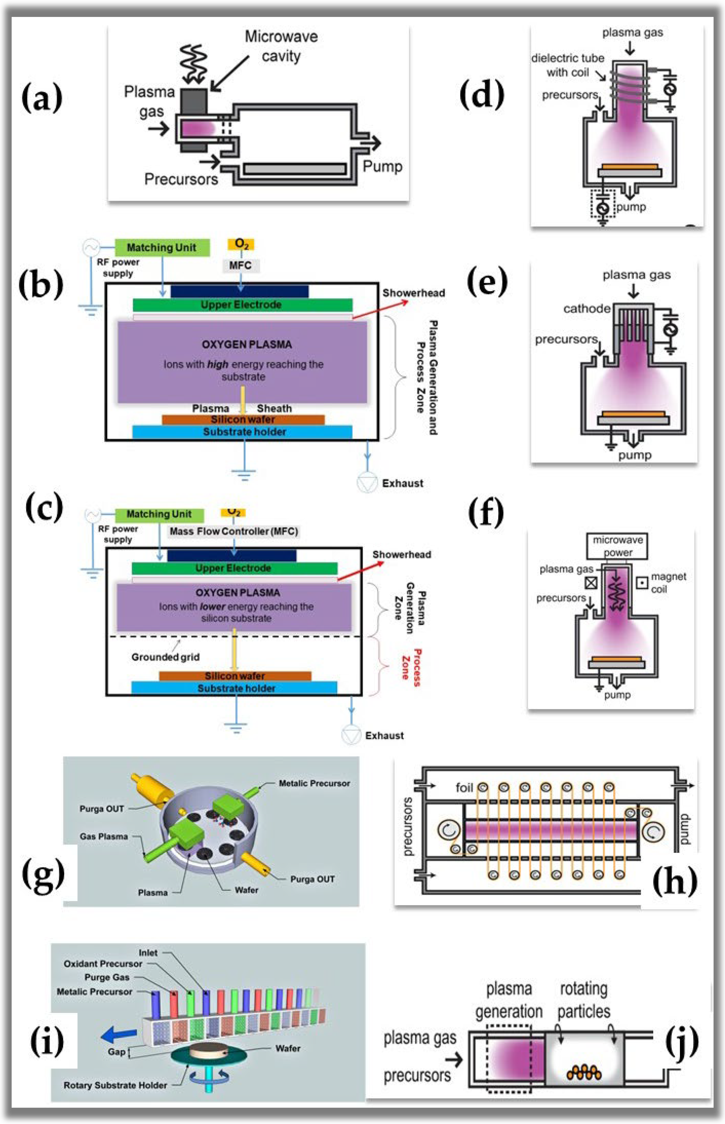
| Nomenclature/Plasma Source | Characteristics |
|---|---|
| Radical-enhanced ALD/Microwave surfatron (Figure 6a) |
|
| Direct mode/Capacitively-coupled plasma (CCP)—without mesh (Figure 6b) |
|
| Remote mode/CCP—with mesh (Figure 6c) |
|
| Remote mode/Inductively-coupled plasma (ICP)—with or without bias (Figure 6d) |
|
| Remote mode/Hollow-cathode (HC) (Figure 6e) |
|
| Remote mode/Microwave electron cyclotron resonance (Figure 6f) |
|
| Carousel mode (Direct)/CCP (Figure 6g) |
|
| Roll-to-roll (Direct)/CCP (Figure 6h) |
|
| Atmospheric Spatial DBD (Dielectric barrier discharge) (Figure 6g) |
|
| Low pressure rotary reactor/HC or ICP (Figure 6i) |
|
| Material Etching | Etching Gas | Additive Gas | Etching Gtoms |
|---|---|---|---|
| Mono and polycrystalline silicon | SF6, NF3, F2, CF4, CHF3, C2F6, SiCl4, CCl4, BCl3, CCl3F, CCl2F2, CBrF3, HBr | CH4, O2, H2, N2, Ar, He | F, Cl, Br |
| SiO2 | SF6, CH4, CHF3, C2F6, C3F8 | CH4, O2, H2, N2, Ar | F, F+C |
| Si3N4 | SF6, CH4, CHF3, C2F6, C3F8 | CH4, O2, H2, N2, Ar | F |
| Resist | O2 | - | O |
| W | SF6, CH4 | O2, Ar | F |
| Al | SiCl4, CCl4, BCl3, Cl2 | Ar | Cl |
| * Al2O3 | HF, SF4, CHF3 | - | F |
| * AlF3 | HF | - | F |
| * AlN | HF | - | F |
| * Co | Cl2, O2 | - | Cl, O |
| * Cu | O3 | - | O |
| * Fe | Cl2 | - | Cl |
| * Ga2O3 | HF | - | F |
| * GaN | XeF2 | - | F |
| GaAs | SiCl4, CCl4, Cl2 | Ar | Cl |
| * Ge | Cl2 | - | Cl |
| * Graphene | O2 | O | |
| * Graphite | O2 | - | O |
| * HfO2 | HF, XeF2, SF4 | - | F |
| * HfZrO2 | HF, XeF2, SF4 | - | F |
| * InGaAs | HF | - | F |
| * InAlAs | HF | - | F |
| * InGaZnO4 | HF | - | F |
| * Mo | O3,HF | - | O, F |
| * Ni | O2, HF | - | O, F |
| * Polymer (Polystyrene) | O2 | - | O |
| * TiN | O3, CHF3/O2 downstream plasma | - | F, F+C, O |
| Phases | Chemical Mechanism | Site of Chemical Mechanisms |
|---|---|---|
| 1 | Reactive species are generated in the plasma by collisional processes between electrons and neutrals, namely, dissociation, dissociative ionization, and dissociative electron capture, among others; | Gas and plasma |
| 2 | these species move from the plasma to the surface of the material to be corroded, by diffusion, in the case of atoms and radicals, and by drift, in the case of ions; | Gas and plasma |
| 3 | reaching the surface, these species are adsorbed; | Surface |
| 4 | the process of chemisorption of the reactive particles takes place on the surface, i.e., chemical bonds are formed; | Surface |
| 5 | these chemical reactions on the surface promote the formation of volatile products; | Surface |
| 6 | these volatile products desorb from the surface and | Surface |
| 7 | return to the plasma by diffusion, from where they are removed by the pumping system (vacuum pump). | Gas and plasma |
Publisher’s Note: MDPI stays neutral with regard to jurisdictional claims in published maps and institutional affiliations. |
© 2022 by the authors. Licensee MDPI, Basel, Switzerland. This article is an open access article distributed under the terms and conditions of the Creative Commons Attribution (CC BY) license (https://creativecommons.org/licenses/by/4.0/).
Share and Cite
Chiappim, W.; Neto, B.B.; Shiotani, M.; Karnopp, J.; Gonçalves, L.; Chaves, J.P.; Sobrinho, A.d.S.; Leitão, J.P.; Fraga, M.; Pessoa, R. Plasma-Assisted Nanofabrication: The Potential and Challenges in Atomic Layer Deposition and Etching. Nanomaterials 2022, 12, 3497. https://doi.org/10.3390/nano12193497
Chiappim W, Neto BB, Shiotani M, Karnopp J, Gonçalves L, Chaves JP, Sobrinho AdS, Leitão JP, Fraga M, Pessoa R. Plasma-Assisted Nanofabrication: The Potential and Challenges in Atomic Layer Deposition and Etching. Nanomaterials. 2022; 12(19):3497. https://doi.org/10.3390/nano12193497
Chicago/Turabian StyleChiappim, William, Benedito Botan Neto, Michaela Shiotani, Júlia Karnopp, Luan Gonçalves, João Pedro Chaves, Argemiro da Silva Sobrinho, Joaquim Pratas Leitão, Mariana Fraga, and Rodrigo Pessoa. 2022. "Plasma-Assisted Nanofabrication: The Potential and Challenges in Atomic Layer Deposition and Etching" Nanomaterials 12, no. 19: 3497. https://doi.org/10.3390/nano12193497