
Enhanced Photocurrent of the Ag Interfaced Topological Insulator Bi2Se3 under UV- and Visible-Light Radiations

1
Department of Materials Science and Engineering, National Chung Hsing University, Taichung 40227, Taiwan
2
International Agriculture Center, National Chung Hsing University, Taichung 40227, Taiwan
3
Department of Electrical and Computer Engineering, Texas A&M University, College Station, TX 77843, USA
4
Department of Chemical Engineering and Materials Science, Chinese Culture University, Taipei 11114, Taiwan
*
Authors to whom correspondence should be addressed.
Nanomaterials 2021, 11(12), 3353; https://doi.org/10.3390/nano11123353
Submission received: 8 November 2021
/
Revised: 5 December 2021
/
Accepted: 8 December 2021
/
Published: 10 December 2021
(This article belongs to the Topic Advances and Applications of 2D Materials)
Abstract
:Bi2Se3 is a topological quantum material that is used in photodetectors, owing to its narrow bandgap, conductive surface, and insulating bulk. In this work, Ag@Bi2Se3 nanoplatelets were synthesized on Al2O3(100) substrates in a two-step process of thermal evaporation and magnetron sputtering. X-ray diffractometer (XRD), high-resolution transmission electron microscopy (HRTEM), Raman spectroscopy, and x-ray photoelectron spectroscopy (XPS) revealed that all samples had the typical rhombohedral Bi2Se3. Field-emission scanning electron microscopy (FESEM)-energy dispersive x-ray spectroscopy (EDS), XPS, and HRTEM confirmed the presence of the precipitated Ag. The optical absorptance of Bi2Se3 nanoplatelets in UV-visible range decreased with the Ag contents. Results of photocurrent measurements under zero-bias conditions revealed that the deposited Ag affected photosensitivity. A total of 7.1 at.% Ag was associated with approximately 4.25 and 4.57 times higher photocurrents under UV and visible light, respectively, than 0 at.% Ag. The photocurrent in Bi2Se3 at 7.1 at.% Ag under visible light was 1.72-folds of that under UV light. This enhanced photocurrent is attributable to the narrow bandgap (~0.35 eV) of Bi2Se3 nanoplatelets, the Schottky field at the interface between Ag and Bi2Se3, the surface plasmon resonance that is caused by Ag, and the highly conductive surface that is formed from Ag and Bi2Se3. This work suggests that the appropriate Ag deposition enhances the photocurrent in, and increases the photosensitivity of, Bi2Se3 nanoplatelets under UV and visible light.
1. Introduction
Bismuth selenide (Bi2Se3) is a material with a narrow bandgap (~0.35 eV), a rhombohedral crystal structure, a unique gapless surface state, and a bulk electronic bandgap [1,2,3,4]. The unique properties of Bi2Se3 arise from the time-reversal symmetry and the spin-orbit coupling, which result in high electronic conductivity at the surface (three-dimensions) and edges (two-dimensions) [5]. Bi2Se3 has the following favorable properties: (1) low power dissipation, (2) photon-like and spin-polarized electrons, and (3) the quantum spin Hall Effect [6,7,8]. Owing to its unique optoelectronic properties, Bi2Se3 can be used in photodetectors [9], spintronic devices [10], and topological superconductors [11,12]. Bulk Bi2Se3 exhibits n-type semiconducting properties owing to the Se vacancies, which supply free electrons that induce a high bulk conductivity and suppress its surface electronic transportation [13,14]. Nanosized Bi2Se3 crystals exhibit a weaker bulk effect and greater electronic transportation because of their high surface-to-volume ratio [15]. The methods for synthesizing nanosized Bi2Se3 include: (1) thermal chemical vapor deposition (CVD) process [16], (2) successive ionic layer adsorption and reaction (SILAR) [17], (3) chemical bath deposition (CBD) [18], (4) electrodeposition [19], and (5) the solvothermal method [20]. Photodetectors are useful in optical information communications, imaging detection, and biodetection owing to the transit between photon and electron [21,22,23]; to be effective, they must have a high photoelectric conversion efficiency. A photodetector should (1) exhibit photo-absorptance over a wide range of wavelengths, (2) high photosensitivity, (3) high free-carrier mobility, (4) high photon-electron conversion efficiency, (5) a low operating voltage, and (6) long-term stability [24,25]. Bi2Se3 satisfies all of the requirements of a potential photodetector owing to its unique surface state and excellent surface electronic transportation. Various methods for enhancing its photocurrent have been reported upon. Pamu et al. found that Au or Ag nanodisks enhance the photocurrent of photosystem I (PSI) as a result of the plasmonic interaction between metal and PSI [26]. Peng et al. found that a semiconductor quantum dot of InAs/GaAs increases the photocurrent in an n-i Schottky device as a result of the Coulomb interaction [27]. Yan et al. found that a textured silicon wafer and periodic Ag nanoarrays increase the photocurrent of the silicon solar cell owing to their textured morphology and plasmonic effect [28]. Chakraborty et al. reported that Au increases the photocurrent in the CdSe nanowires owing to the plasmonic effect and Schottky field at the interface between the metal and the semiconductor [29]. These reports suggest that the photocurrent can be enhanced by the plasmonic effect, the Schottky field, and surface morphology. The photocurrent in, and enhancements of, Bi2Se3 have been studied and reported [30,31,32]. Wang et al. applied external strain to Bi2Se3 nanowires and thereby increased the photocurrent therein [33]. Gupta et al. found that the Ag nanoparticle-decorated Bi2Se3 that was synthesized by a chemical solution method exhibited an enhanced photocurrent at a bias of −10 V [34]. Chae et al. found that Bi2Se3/graphene exhibited an enhanced photocurrent with a source-drain voltage of 1.5V [35]. Liao et al. found that reduced graphene oxide increased the photocurrent of Bi2Se3 nanosheets [36]. Based on the enhancing factors of the plasmonic effect and the interaction between metal and semiconductors, the thermal CVD process that involves a catalyst-free vapor-solid mechanism is used herein to synthesize Bi2Se3 nanoplatelets, on which Ag is deposited by magnetron sputtering. The enhancement of the photocurrent in the Bi2Se3 nanoplatelets under UV and visible light by Ag was studied.
2. Materials and Methods
2.1. Fabrication of Pristine Bi2Se3 and Ag@Bi2Se3 Nanoplatelets
Pristine Bi2Se3 nanoplatelets were fabricated on an Al2O3 (100) substrate (0.5 × 0.5 mm2) using a catalyst-free vapor-solid mechanism by thermal evaporation in a quartz tube furnace. A mixture of precursor powders of 0.1g bismuth (purity = 99%, 4.78 × 10⁻⁴ mole, Merck, Darmstadt, Germany) and 0.1g selenium (purity = 99%, 1.27 × 10⁻³ mole, Alfa Aesar, Ward Hill, MA, USA) were placed in an alumina boat, which was placed in the heating zone at the center of the quartz tube and heated to 600 °C at a rate of 25 °C/min under 1.5 × 10⁻² Torr, in which conditions were maintained for 60 min. The Al2O3 (100) substrate was placed upstream in the quartz tube at about 140 °C, 21 cm away from the alumina boat. Thus, pristine Bi2Se3 nanoplatelets were grown on the Al2O3 (100) substrate. Then, the synthesized system was slowly cooled to room temperature after a 60 min deposition process. An Ag thin film was deposited on a sapphire substrate for 60 s (110V, 4 mA) at 1 × 10⁻¹ mbar. It was then measured using a profilometer (Dektak XT, Bruker, Billerica, MA, USA) to estimate the Ag deposition rate. Then, Ag was deposited on the Bi2Se3 nanoplatelets at a working distance of 35 mm by magnetron sputtering (110 V, 4 mA) using a 2-inch Ag target at room temperature under 1 × 10⁻¹ mbar. Ag was deposited for 10, 15, 20, and 25s yielding Ag10s@Bi2Se3, Ag15s@Bi2Se3, Ag20s@Bi2Se3, and Ag25s@Bi2Se3 nanoplatelets, respectively.
2.2. Characterization of Nanoplatelets
The crystal structures of the pristine Bi2Se3 and Ag@Bi2Se3 nanoplatelets were determined using XRD (λ = 0.154 nm, 30 A, 40 kV, Bruker D2 PHASER) at 2θ = 10–60°, and HRTEM (JEOL JEM-2010, Tokyo, Japan). XPS (PerkinElmer model PHI1600 system, Waltham, MA, USA) and Raman spectroscopy (3D Nanometer Scale Raman PL Microspectrometer, Tokyo Instruments, INC., Tokyo, Japan) with a semiconductor laser (λ = 488 nm) were used to record the chemical binding energies and vibration modes of the chemical bonds. The surface morphology and EDS spectra of the pristine Bi2Se3 and Ag@Bi2Se3 nanoplatelets were obtained using FESEM (ZEISS Ultra Plus, Carl Zeiss Microscopy GmbH, Oberkochen, Germany). The optical absorptance of UV and visible light was recorded using a UV-visible spectrometer (Hitachi U3900-H, Hitachi Ltd., Tokyo, Japan) that was equipped with an integrating sphere.
2.3. Photocurrent Measurements
A semiconductor I-V characterizing analyzer (Keysight B2901A Precision Source/Measure Unit 100 fA, Keysight Technologies, Santa Rosa, CA, USA) recorded the photocurrents at 0 V bias under UV- and visible-light in the ambient environment. The sources of incident light were 30 cm-long UV (8 W, λ = 365 nm) and visible light (8 W, λ = 380–780 nm) LED lamps at 20 cm from the sample. The photocurrents in all samples were recorded in a dark room to eliminate any effect from stray lights. Silver paste was used as an electrode that was connected to a current analyzer using copper wires. The photocurrent in each sample was measured six times; each time, the light was on for 10 s and off for 10 s.
3. Results
3.1. XPS Analysis
Figure 1 present the XPS spectra of the Bi 4f, Se 3d, and Ag 3d of the pristine and Ag25s@Bi2Se3 nanoplatelets. Figure 1a display the spectra of the Bi 4f orbit of the pristine Bi2Se3 and Ag25s@Bi2Se3 nanoplatelets, revealing four significant peaks. The peaks at 157.94 and 163.26 eV are associated with the Bi 4f7/2 and Bi 4f5/2 in Bi2Se3 [16]; those at 158.69 and 164.30 eV correspond to the binding energies of the Bi–O phase in Bi2O3 [37]. Figure 1b show the XPS of Bi 4f in the pristine Bi2Se3 and Ag25s@Bi2Se3 nanoplatelets, from which the peaks are in similar positions. Figure 1c and d present the Se 3d orbits of the pristine Bi2Se3 and Ag25s@Bi2Se3 nanoplatelets. Three main peaks at 53.5, 54.3, and 55.1 eV are observed. The first two peaks correspond to Se 3d5/2 and Se 3d3/2 in Bi2Se3 [38], and the last one corresponds to the metal Se [39]. The metallic Se traps the free electrons and suppresses the photocurrent that arises from them. A weak peak at 58.66 eV is observed in Figure 1d, arising from the Se–O bonds [40]. These XPS spectra confirm the formation of the Bi2Se3 structure. The peaks of Bi–O and Se–O are attributed to natural formations on the surface of the sample in an ambient environment. Figure 1e present the Ag 3d binding energy in Ag25s@Bi2Se3 nanoplatelets. Peaks at 367.55 and 373.58 eV with an energy separation of 6.03 eV correspond to the Ag 3d5/2 and Ag 3d3/2 of metallic Ag. The binding energies of Ag 3d5/2 and Ag 3d3/2 are lower than that of bulk Ag (~368 eV). The shift of the binding energy is relative to the electronegativity of the elements and is responsible for the change in the charge around the atom [41]. The larger electronegativity of the element, the blue-shift of the binding energy. Ag (1.93) has a lower electronegativity than Bi (2.02) and Se (2.55). Therefore, the binding energies of Ag 3d5/2 and Ag 3d3/2 shift toward lower energy (red-shift). Table 1 show the atomic percentages of Bi, Se, and Ag, confirming the presence of Ag; the portion of Ag increases with the deposition time.
3.2. Morphological Analysis
Figure 2a,b present the morphologies of the pristine Bi2Se3 and Ag25s@Bi2Se3 nanoplatelets that are obtained using FESEM. Both samples have a hexagonal structure which is typical of rhombohedral Bi2Se3. FESEM-EDS detects the presence of Ag along with the Bi and Se. The estimated thickness (40 nanoplatelets) and size (40 nanoplatelets) of each nanoplatelet of pristine Bi2Se3 is 6.9 and 8.3 nm; those of Ag25s@Bi2Se3 are 444.8 and 488.5nm, respectively. Bi2Se3 has the same layered structures as graphite. Each layer comprises five stacked atomic layers Se1–Bi–Se2–Bi–Se1 and is called the quintuple layer (QL). The thickness of each QL is 0.955 nm [42], indicating that pristine Bi2Se3 and Ag25s@Bi2Se3 nanoplatelets have 7.22 and 8.69 OLs, respectively. Figure 2c present the thickness of the Ag thin film that is deposited on a sapphire substrate at 0.44W for 60s (110 V, 4 mA) at 1 × 10⁻¹ mbar. The ideal Ag thicknesses in pristine Bi2Se3, Ag10s, Ag15s, Ag20s, and Ag25s@Bi2Se3 nanoplatelets are 0, 3.3, 5, 6.7, and 8.3 nm, respectively. Therefore, the Ag was not easily observed in the FESEM images.
3.3. Analysis of Crystal Structures and Surface Morphologies
Figure 3 present the XRD patterns of the pristine Bi2Se3 and Ag@Bi2Se3 nanoplatelets. Nine significant peaks are observed at 2θ values of 18.55°, 25.03°, 27.91°, 29.39°, 40.28°, 43.07°, 43.77°, 47.67°, and 53.61°, corresponding to the planes (006), (101), (104), (015), (1010), (0111), (110), (0015), and (205) of the rhombohedral Bi2Se3 structure (JCPDS 89-2008). No significant peak of oxides or silver are observed because the content of oxides and Ag are less than the limit of detection (~5%) by XRD. The grain sizes of pristine Bi2Se3 and Ag@Bi2Se3 nanoplatelets are estimated at 14.56±7.9% nm using the Williamson-Hall equation [43] and plotted in the inset in Figure 3. Table 2 present the lattice constants a (= b) and c and the c/a ratios of the Bi2Se3 nanoplatelets with various Ag contents.
Figure 4a–c present the HRTEM images and selected area diffraction (SAD) patterns of the pristine Bi2Se3 nanoplatelets. Figure 4a present the hexagonal morphology that is typical of rhombohedral Bi2Se3. The d-spacings of 0.334 and 0.317 are estimated from Figure 4b, corresponding to the Bi2Se3 (012) and Bi2Se3 (009) planes. Figure 4c present the SAD patterns and reveals Bi2Se3 (101), Bi2Se3 (012), and Bi2Se3 (110) planes. Figure 4d–f present HRTEM images and SAD patterns of Ag25s@Bi2Se3 nanoplatelets. Figure 4d show that the Ag20s@Bi2Se3 nanoplatelets have the same morphology as the pristine ones, which is shown in Figure 4a. Figure 4e reveal the estimated d-spacings of 0.341 and 0.207 nm, which correspond to Bi2Se3 (012) and Ag (200), respectively, as shown in the blue-line region in Figure 4e. Figure 4f present the SAD pattern of Ag20s@Bi2Se3 nanoplatelets, which corresponds to the Bi2Se3 (012), Bi2Se3 (009), and Bi2Se3 (110) planes. The results of XRD and HRTEM reveal that the crystal structures of pristine Bi2Se3 and Ag20s@Bi2Se3 nanoplatelets are the typical rhombohedral Bi2Se3 structure. The Ag phase is also observed in Figure 4e.
3.4. Raman Analysis
Figure 5a,b present two typical Raman peaks of rhombohedral Bi2Se3 at and from the pristine Bi2Se3 and Ag25s@Bi2Se3 nanoplatelets [16]. Bi2Se3 belongs to the space group (). The atoms in a QL are bonded covalently [44]; Van der Waals forces bind the QLs [16]. The zone-center phonon formula of Bi2Se3 is [42], where and are the Raman-active modes and and are the infrared-active modes. The mode is the out-of-plane stretching symmetry mode with the vibration of the Se1 and Bi1 atoms in opposite directions. Therefore, the mode has a short displacement (Figure 5a). The mode is the in-plane bending symmetry mode shearing the upper Se1 and Bi1 atomic layers, which vibrate with a longer displacement than in the mode and have a large binding energy (Figure 5a) [45]. These results suggest that the rhombohedral Bi2Se3 formed successfully, and the Ag has no significant effect on the binding structure.
3.5. Analysis of Optical Properties
Figure 6a present the absorptance spectrum of the pristine Bi2Se3 and Ag@Bi2Se3 nanoplatelets. The absorptance of the nanoplatelets decreases as the Ag deposition time increases. Figure S1 reveal the absorptance of Ag/Bi2Se3 thin film as simulated in TFCalc software. The simulation involves (1) a Bi2Se3 thin film with a thickness of 10 nm, (2) Ag thin films with a thickness of 0, 2, 4, 6, 8, and 10 nm, and (3) a sapphire substrate. The absorptance of the Ag@Bi2Se3 thin films decreases as the Ag thickness increases, consistent with the experimental results (Figure 6a). This decrease in absorptance is attributed to the increase in reflectance by the decoration with Ag. The absorptance of the Ag@Bi2Se3 nanoplatelets is therefore suppressed. Figure 6b present the normalized absorptance at various Ag deposition times. The Ag@Bi2Se3 nanoplatelets have a broad band from 375 to 420 nm that is centered at ~398 nm.
In order to understand the effect of the Ag thin film on the optical absorptance of Bi2Se3, a simulation is performed, and its results are presented in Figure S2. The simulated structure is a Au thin film/Bi2Se3 thin film (10 nm)/sapphire substrate. The simulation involves (1) Ag thin films with a thickness of 0, 2, 4, 6, 8, and 10 nm, and (2) a sapphire substrate. A significant peak at 400 nm is observed while the Ag thickness increases, as shown in Figure S2, consistent with the experimental results (Figure 6b). The broad peak from 375 to 420 nm that is centered at ~398 nm (Figure 6b) is therefore confirmed to be caused by the Ag and attributable to the surface plasmon resonance [46].
3.6. Photocurrent under the UV and Visible Light
Figure 7a,b plot the measured photocurrents under UV (8 W, λ = 365 nm) and visible light (8 W, λ = 380–780 nm); the measurements are performed six times. Each measurements cycle lasts 20 s, comprising 10 s under illumination and 10 s without illumination. The substrate bias is 0 voltage during the measurement of photocurrent; therefore, the photocurrents are spontaneously generated by the incident light. The photocurrents in pristine Bi2Se3 under UV and visible light are lower than those in the Ag@Bi2Se3 nanoplatelets, as shown in Figure 7a,b. The photocurrent increases with Ag content from 0 to 7.1 at.%, and then decreases as the Ag content increases further to 8.2 at.%. Figure 7c plot the photocurrent as a function of Ag content. The highest photocurrents at 7.1 at.% Ag exceed those in the pristine nanoplatelets by factors about 4.25 and 4.57 under UV and visible light, respectively. Additionally, the photocurrents at 7.1 at.% Ag under visible light exceed those under UV light by a factor of about 1.7. These results reveal that a particular Ag content can increase the photocurrent in Bi2Se3 nanoplatelets under UV and visible light and that Ag@Bi2Se3 nanoplatelets have higher photosensitivity under visible light than that under UV light.
3.7. Mechanism of Photocurrent Enhancement
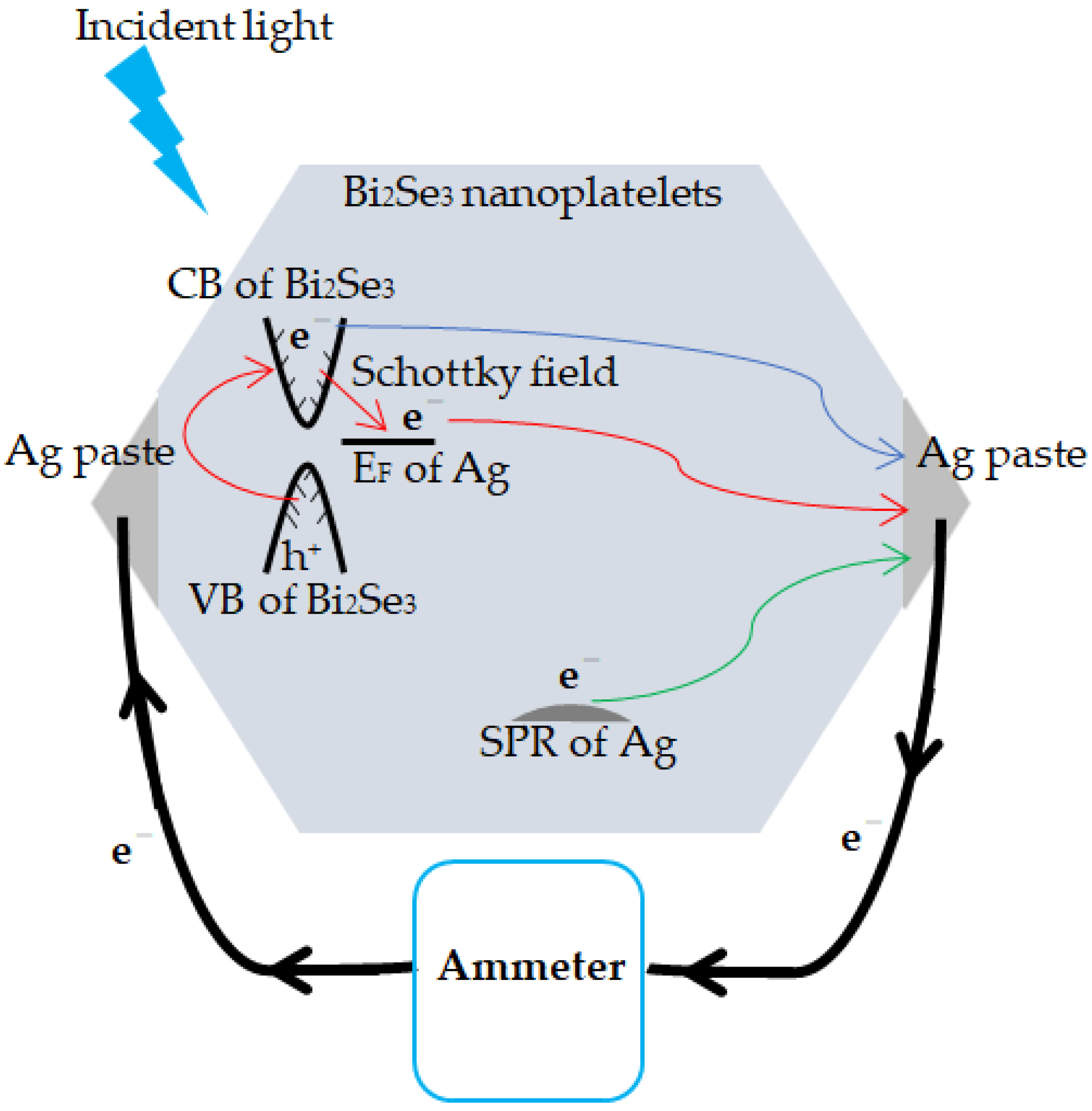
Bi2Se3 is a semiconductor with a narrow bandgap (~0.35 eV) [47], in which the photo-induced electron-hole pairs are readily generated by UV and visible light. A Schottky field can be formed at the interface between Ag and Bi2Se3, and it dissociates the photo-induced electrons and holes in Bi2Se3 [29]. This dissociation process generates free electrons and suppresses their recombination with holes. Surface plasmon resonance (SPR) (Figure 6b) is observed in the Ag@Bi2Se3 nanoplatelets. SPR is the collective oscillation of electrons in the conduction band after the absorption of light with a particular incident energy, generating unstable/free electrons. These free electrons can be smoothly transported at the conductive surface that contributed to the Ag and nanosized Bi2Se3 platelets [15], enhancing the photocurrent. This photocurrent enhancement has the following causes: (1) the narrow bandgap of the pristine Bi2Se3 nanoplatelets, (2) the Schottky field at the interface between Ag and Bi2Se3, (3) the SPR effect of the Ag decoration, and (4) the highly conductive surface contributing to the Ag and Bi2Se3 nanoplatelets. Figure 8 present the proposed transmission path.
Notably, the photocurrent under visible light exceeds that under UV. The absorptance of nanoplatelets under visible light exceeds that under UV (Figure 6a), indicating that visible light can be efficiently used by the nanoplatelets. The high-energy incident light (UV) generates high concentrations of free carriers close to the surface. These free carriers then recombine through surface states because of the high carrier density, reducing the total photocurrent [48]. A high Ag content (8.1 at.%) is associated with lower photocurrent under UV or visible light. The SPR enhances the near-field intensity and increases the concentrations of unstable/free electrons. Therefore, higher densities of electrons are generated in the surface region, and these electrons subsequently recombine with the holes, suppressing the photocurrent.
4. Conclusions
The Ag@Bi2Se3 nanoplatelets exhibit a significantly higher photocurrent under UV and visible light. The photocurrents of Ag@Bi2Se3 nanoplatelets with 7.1 at.% Ag under UV and visible light were approximately 4.25 and 4.57 times larger than those in pristine Bi2Se3 nanoplatelets. The resulting photocurrent in the Ag@Bi2Se3 nanoplatelets with 7.1 at.% Ag under visible light is 1.72-fold compared to that of pristine nanoplatelets under UV light. The presence of Ag and metallic Se is confirmed by XPS, FESEM, and HRTEM images. Free electrons are trapped by metallic Se, reducing the photocurrent. The rhombohedral Bi2Se3 crystal structure is confirmed by XRD, HRTEM, and Raman spectra. The Ag decoration has no effect on the Bi2Se3 crystal structure. The absorptance that is recorded by the UV-visible spectrometer reveals that increasing the Ag content reduces their total absorptance, affecting their light-to-electron transformation efficiency, suppressing the generation of the photocurrent. The SPR effect of Ag is evident in the absorptance spectra; it generates unstable/free electrons, enhancing the photocurrent in the nanoplatelets. The appropriate Ag content significantly enhances the photocurrent of pristine Bi2Se3 nanoplatelets because of the following: (1) the narrow bandgap of Bi2Se3 nanoplatelets, (2) the Schottky field at the interface between Ag and Bi2Se3, (3) the surface plasmon resonance that is caused by Ag, and (4) the highly conductive surface. The photocurrent was suppressed for the following reasons: (1) the high carrier densities that are generated by the high-energy incident light and SPR increase the rate of recombination between electrons and holes; (2) metallic Se may act as a recombination center; and (3) the absorptance of the Bi2Se3 nanoplatelets is reduced by Ag decoration. This work suggests that the incorporation of a particular amount of Ag enhances the photocurrent in Ag@Bi2Se3 nanoplatelets; this phenomenon may have immediate application in the detection of UV and visible light.
Supplementary Materials
The following are available online at https://www.mdpi.com/article/10.3390/nano11123353/s1, Figure S1: (a–f) are the simulated absorptance spectra of the Ag@Bi2Se3 thin film while Ag thin film at 0, 2, 4, 6, 8, and 10 nm, Figure S2: (a–f) are the simulated absorptance spectra of Ag thin film in 0, 2, 4, 6, 8, and 10 nm.
Author Contributions
Conceptualization, F.-S.S. and H.-C.S.; methodology, F.-S.S., H.-C.S., P.-T.L. and C.-C.W.; software, C.-C.W.; validation, C.-C.W.; formal analysis, C.-C.W. and P.-T.L.; investigation, C.-C.W.; resources, H.-C.S. and F.-S.S.; data curation, C.-C.W. and P.-T.L.; writing—original draft preparation, C.-C.W.; writing-review and editing, P.-T.L., H.-C.S. and F.-S.S.; visualization, C.-C.W.; supervision, H.-C.S. and F.-S.S.; project administration, H.-C.S.; funding acquisition, H.-C.S. All authors have read and agreed to the published version of the manuscript.
Funding
This research was funded by the Ministry of Science and Technology (MOST) of Taiwan, Republic of China, grant number MOST 110-2221-E-034-006, and the Higher Education Sprout Project (HESP), Ministry of Education (MOE), Taiwan, R.O.C under the contract 110S0802C.
Institutional Review Board Statement
Not applicable.
Informed Consent Statement
Not applicable.
Data Availability Statement
Data is contained within the article.
Acknowledgments
The authors gratefully acknowledge the financial support of the Ministry of Science and Technology (MOST) of Taiwan, Republic of China, and the Higher Education Sprout Project (HESP), Ministry of Education (MOE), Taiwan, R.O.C.
Conflicts of Interest
The authors declare no conflict of interest.
References
- Nechaev, I.A. Evidence for a direct band gap in the topological insulator Bi2Se3 from theory and experiment. Phys. Rev. B Condens. Matter Mater. Phys. 2013, 87, 121111. [Google Scholar] [CrossRef] [Green Version]
- Liu, X.; Xu, J.; Fang, Z.; Lin, L.; Qian, Y.; Wang, Y.; Ye, C.; Ma, C.; Zeng, J. One-pot synthesis of Bi2Se3 nanostructures with rationally tunable morphologies. Nano Res. 2015, 8, 3612–3620. [Google Scholar] [CrossRef]
- Kane, C.L.; Mele, E.J.Z. Topological order and the quantum spin Hall effect. Phys. Rev. Lett. 2005, 95, 146802. [Google Scholar] [CrossRef] [PubMed] [Green Version]
- Konig, M.; Wiedmann, S.; Brune, C.; Roth, A.; Buhmann, H.; Molenkamp, L.W.; Qi, X.L.; Zhang, S.C. Quantum spin Hall insulator state in HgTe quantum wells. Science 2007, 318, 766–770. [Google Scholar] [CrossRef] [PubMed] [Green Version]
- Irfan, B.; Sahoo, S.; Gaur, A.P.S.; Ahmadi, M.; Guinel, M.J.F.; Katiyar, R.S.; Chatterjee, R. Temperature dependent Raman scattering studies of three dimensional topological insulators Bi2Se3. J. Appl. Phys. 2014, 115, 173506. [Google Scholar] [CrossRef]
- Fei, F.; Zhang, S.; Zhang, M.; Shah, S.A.; Song, F.; Wang, X.; Wang, B. The material efforts for quantized Hall devices based on topological insulators. Adv. Mater. 2020, 32, 1904593. [Google Scholar] [CrossRef]
- Mishra, S.K.; Satpathy, S.; Jepsen, O. Electronic structure and thermoelectric properties of bismuth telluride and bismuth selenide. J. Phys. Condens. Matter. 1997, 9, 461–470. [Google Scholar] [CrossRef]
- Tian, W.; Yu, W.; Shi, J.; Wang, Y. The property, preparation and application of topological insulators: A review. Materials 2017, 10, 814. [Google Scholar] [CrossRef] [Green Version]
- Wang, F.; Li, L.; Huang, W.; Li, L.; Jin, B.; Li, H.; Zhai, T. Submillimeter 2D Bi2Se3 flakes toward high-performance infrared photodetection at optical communication wavelength. Adv. Funct. Mater. 2018, 28, 1802707. [Google Scholar] [CrossRef]
- Tian, J.; Şahin, C.; Miotkowski, I.; Flatté, M.E.; Chen, Y.P. Opposite current-induced spin polarizations in bulk-metallic Bi2Se3 and bulk-insulating Bi2Te2Se topological insulator thin flakes. Phys. Rev. B 2021, 103, 035412. [Google Scholar] [CrossRef]
- Kong, P.P.; Zhang, J.L.; Zhang, S.J.; Zhu, J.; Liu, Q.Q.; Yu, R.C.; Fang, Z.; Jin, C.Q.; Yang, W.G.; Yu, X.H.; et al. Superconductivity of the topological insulator Bi2Se3 at high pressure. J. Phys. Condens. Matter 2013, 25, 362204. [Google Scholar] [CrossRef] [PubMed]
- Yonezawa, S. Nematic superconductivity in doped Bi2Se3 topological superconductors. Condens. Matter 2019, 4, 2. [Google Scholar] [CrossRef] [Green Version]
- Kim, D.; Cho, S.; Butch, N.P.; Syers, P.; Kirshenbaum, K.; Adam, S.; Paglione, J.; Fuhrer, M.S. Surface conduction of topological Dirac electrons in bulk insulating Bi2Se3. Nat. Phys. 2012, 8, 459–463. [Google Scholar] [CrossRef] [Green Version]
- Jia, S.; Beidenkopf, H.; Drozdov, I.; Fuccillo, M.K.; Seo, J.; Xiong, J.; Ong, N.P.; Yazdani, A.; Cava, R.J. Defects and high bulk resistivities in the Bi-rich tetradymite topological insulator Bi2+xTe2−xSe. Phys. Rev. B 2012, 86, 165119. [Google Scholar] [CrossRef]
- Schönherr, P.; Collins-McIntyre, L.J.; Zhang, S.; Kusch, P.; Reich, S.; Giles, T.; Daisenberger, D.; Prabhakaran, D.; Hesjedal, T. Vapour-liquid-solid growth of ternary Bi2Se2Te nanowires. Nanoscale Res. Lett. 2014, 9, 127. [Google Scholar] [CrossRef] [Green Version]
- Wang, C.C.; Shieu, F.S.; Shih, H.C. Photosensing and characterizing of the pristine and In-, Sn-doped Bi2Se3 nanoplatelets fabricated by thermal V–S process. Nanomaterials 2021, 11, 1352. [Google Scholar] [CrossRef]
- Ahmed, R.; Xu, Y.; Sales, M.G.; Lin, Q.; McDonnell, S.; Zangari, G. Synthesis and material properties of Bi2Se3 nanostructures deposited by SILAR. J. Phys. Chem. C 2018, 122, 12052–12060. [Google Scholar] [CrossRef]
- Wang, W.; Wang, X.; Wang, N.; Ning, X.; Li, H.; Lu, D.; Liu, X.; Zhang, Q.; Huang, Y. Bi2Se3 sensitized TiO2 nanotube films for photogenerated cathodic protection of 304 stainless steel under visible light. Nanoscale Res. Lett. 2018, 13, 295. [Google Scholar] [CrossRef] [PubMed] [Green Version]
- Souza, P.B.; Tumelero, M.A.; Zangari, G.; Pasa, A.A. Tuning electrodeposition conditions towards the formation of smooth Bi2Se3 thin films. J. Electrochem. Soc. 2017, 164, D401–D405. [Google Scholar] [CrossRef]
- Liang, K.; Wang, C.; Xu, X.; Leng, J.; Ma, H. Capacitive and photocatalytic performance of Bi2Se3 nanostructures synthesized by solvothermal method. Phys. Lett. A 2017, 381, 652–657. [Google Scholar] [CrossRef]
- Li, X.M.; Zhao, K.; Ni, H.; Zhao, S.Q.; Xiang, W.F.; Lu, Z.Q.; Yue, Z.J.; Wang, F.; Kong, Y.C.; Wong, H.K. Voltage tunable photodetecting properties of La0.4Ca0.6MnO3 films grown on miscut LaSrAlO4 substrates. Appl. Phys. Lett. 2010, 97, 044104. [Google Scholar] [CrossRef]
- Huang, S.M.; Huang, S.J.; Yan, Y.J.; Yu, S.H.; Chou, M.; Yang, H.W.; Chang, Y.S.; Chen, R.S. Extremely high-performance visible light photodetector in the Sb2SeTe2 nanoflake. Sci. Rep. 2017, 7, 45413. [Google Scholar] [CrossRef] [Green Version]
- Sharma, A.; Bhattacharyya, B.; Srivastava, A.K.; Senguttuvan, T.D.; Husale, S. High performance broadband photodetector using fabricated nanowires of bismuth selenide. Sci. Rep. 2016, 6, 19138. [Google Scholar] [CrossRef] [Green Version]
- Bhattacharyya, B.; Sharma, A.; Kaur, M.; Singh, B.P.; Husale, S. Highly responsive broadband photodetection in topological insulator-Carbon nanotubes based heterostructure. J. Alloys Compd. 2021, 851, 156759. [Google Scholar] [CrossRef]
- Zhang, H.; Song, Z.; Li, D.; Xu, Y.; Li, J.; Bai, C.; Man, B. Near-infrared photodetection based on topological insulator P-N heterojunction of SnTe/ Bi2Se3. Appl. Surf. Sci. 2020, 509, 145290. [Google Scholar] [CrossRef]
- Pamu, R.; Lawrie, B.J.; Khomami, B.; Mukherjee, D. Broadband plasmonic photocurrent enhancement from photosystem I assembled with tailored arrays of Au and Ag nanodisks. ACS Appl. Nano Mater. 2021, 4, 1209–1219. [Google Scholar] [CrossRef]
- Peng, K.; Wu, S.; Xie, X.; Yang, J.; Qian, C.; Song, F.; Sun, S.; Dang, J.; Yu, Y.; Shi, S.; et al. Giant photocurrent enhancement by coulomb interaction in a single quantum dot for energy harvesting. Phys. Rev. Appl. 2019, 11, 024015. [Google Scholar] [CrossRef] [Green Version]
- Yan, W.; Tao, Z.; Gu, M.; Richards, B.S. Photocurrent enhancement of ultrathin front-textured crystalline silicon solar cells by rear-located periodic silver nanoarrays. Sol. Energy 2017, 150, 156–160. [Google Scholar] [CrossRef]
- Chakraborty, R.; Greullet, F.; George, C.; Baranov, D.; Fabrizio, E.D.; Krahne, R. Broad spectral photocurrent enhancement in Au-decorated CdSe nanowires. Nanoscale 2013, 5, 5334. [Google Scholar] [CrossRef]
- Meyer, N.; Geishendorf, K.; Walowski, J.; Thomas, A.; Munzenberg, M. The impact of metallic contacts on spin-polarized photocurrents in topological insulator Bi2Se3 nanowires. Appl. Phys. Lett. 2020, 117, 262401. [Google Scholar] [CrossRef]
- Hong, X.; Shen, J.; Tang, X.; Xie, Y.; Su, M.; Tai, G.; Yao, J.; Fu, Y.; Ji, J.; Liu, X.; et al. High-performance broadband photodetector with in-situ-grown Bi2Se3 film on micropyramidal Si substrate. Opt. Mater. 2021, 117, 111118. [Google Scholar] [CrossRef]
- Xiao, L.; Liu, Q.; Zhang, M.; Liu, L. Photoelectric properties of Bi2Se3 films grown by thermal evaporation method. Mater. Res. Express 2020, 7, 016429. [Google Scholar] [CrossRef]
- Wang, X.; Dai, G.; Liu, B.; Zou, H.; Chen, Y.; Mo, X.; Li, X.; Sun, J.; Liu, Y.; Liu, Y.; et al. Broadband photodetectors based on topological insulator Bi2Se3 nanowire with enhanced performance by strain modulation effect. Phys. E Low-Dimens. Syst. Nanostruct. 2019, 114, 113620. [Google Scholar] [CrossRef]
- Gupta, A.; Chowdhury, R.K.; Ray, S.K.; Srivastava, S.K. Selective photoresponse of plasmonic silver nanoparticle decorated Bi2Se3 nanosheets. Nanotechnology 2019, 30, 435204. [Google Scholar] [CrossRef] [PubMed]
- Chae, J.; Hong, S.B.; Kim, D.; Kim, D.K.; Kim, J.; Jeong, K.; Park, S.H.; Cho, M.H. Enhancement of photoresponse in Bi2Se3/graphene heterostructures by effective electron—Hole separation through internal band bending. Appl. Surf. Sci. 2021, 554, 149623. [Google Scholar] [CrossRef]
- Liao, G.; Zhou, Y.; Huang, Z.; Ma, Q.; Luo, S.; Liu, Y.; Qi, X. Bi2Se3 nanosheets hybridized with reduced graphene oxide for enhanced photoelectrochemical activity. Appl. Phys. A 2021, 127, 705. [Google Scholar] [CrossRef]
- Meng, A.; Yuan, X.; Shen, T.; Li, Z.; Jiang, Q.; Xue, H.; Lin, Y.; Zhao, J. One-step synthesis of flower-like Bi2O3/Bi2Se3 nanoarchitectures and NiCoSe2/Ni0.85Se nanoparticles with appealing rate capability for the construction of high-energy and long-cycle-life asymmetric aqueous batteries. J. Mater. Chem. A 2019, 7, 17613. [Google Scholar] [CrossRef]
- Zhang, G.; Qin, H.; Teng, J.; Guo, J.; Guo, Q.; Dai, X.; Fang, Z.; Wu, K. Quintuple-layer epitaxy of thin films of topological insulator Bi2Se3. Appl. Phys. Lett. 2009, 95, 053114. [Google Scholar] [CrossRef] [Green Version]
- Wagner, C.D.; Riggs, W.M.; Davis, L.E.; Moulder, J.F.; Muilenberg, G.E. Hand Book of X-ray Photoelectron Spectroscopy; Perkin-Elmer Corporation: Eden Prairie, MN, USA, 1979; p. 92. [Google Scholar]
- Hobbs, R.G.; Schmidt, M.; Bolger, C.T.; Georgiev, Y.M.; Fleming, P.; Morris, M.A.; Petkov, N.; Holmes, J.D.; Xiu, F.; Wang, K.L.; et al. Resist–substrate interface tailoring for generating high-density arrays of Ge and Bi2Se3 nanowires by electron beam lithography. J. Vac. Sci. Technol. B 2012, 30, 041602. [Google Scholar] [CrossRef] [Green Version]
- Lamb, R.N.; Ngamsom, B.; Trimm, D.L.; Gong, B.; Silveston, P.L.; Praserthdam, P. Surface characterisation of Pd–Ag/Al2O3 catalysts for acetylene hydrogenation using an improved XPS procedure. Appl. Catal. A-Gen. 2004, 268, 43–50. [Google Scholar] [CrossRef]
- Zhang, J.; Peng, Z.; Son, A.; Zhao, Y.; Xiong, Y.; Peng, B.; Wang, J.; Dresselhaus, M.S.; Xiong, Q. Raman spectroscopy of few-quintuple layer topological insulator Bi2Se3 nanoplatelets. Nano Lett. 2011, 11, 2407–2414. [Google Scholar] [CrossRef] [PubMed]
- Mote, V.D.; Purushotham, Y.; Dole, B.N. Williamson-Hall analysis in estimation of lattice strain in nanometer-sized ZnO particles. J. Theor. Appl. Phys. 2012, 6, 6. [Google Scholar] [CrossRef] [Green Version]
- Zhang, M.; Liu, L.G.; Wang, D.; An, X.Y.; Yang, H. Enhancement of surface state contribution in cadmium doped Bi2Se3 single crystal. J. Alloys Compd. 2019, 806, 180–186. [Google Scholar] [CrossRef]
- Yuan, J.; Zhao, M.; Yu, W.; Lu, Y.; Chen, C.; Xu, M.; Li, S.; Loh, K.P.; Bao, Q. Raman spectroscopy of two-dimensional Bi2TexSe3–x platelets produced by solvothermal method. Materials 2015, 8, 5007–5017. [Google Scholar] [CrossRef] [PubMed]
- Gharibshahi, L.; Saion, E.; Gharibshahi, E.; Shaari, A.H.; Matori, K.A. Structural and optical properties of Ag nanoparticles synthesized by thermal treatment method. Materials 2017, 10, 402. [Google Scholar] [CrossRef] [PubMed]
- Lawal, A.; Shaari, A.; Ahmed, R.; Jarkoni, N. First-principles many-body comparative study of Bi2Se3 crystal: A promising candidate for broadband photodetector. Phys. Lett. A 2017, 381, 2993–2999. [Google Scholar] [CrossRef]
- Ba, X.J.; Schlesinger, T.E.; James, R.B. Chapter 4-Electrical properties of mercuric iodide. In Semiconductors and Semimetals: A Treatise; Willardson, R.K., Beer, A.C., Weber, E.R., Eds.; Academic Press: Millbrae, CA, USA, 1995; Volume 43, pp. 111–168. [Google Scholar]
Figure 1.
XPS spectra of Bi 4f, Se 3d of Bi2Se3 of (a,c), and of Ag25s@Bi2Se3 of (b,d); (e) Ag 3d of Ag25s@Bi2Se3 nanoplatelets.
Figure 1.
XPS spectra of Bi 4f, Se 3d of Bi2Se3 of (a,c), and of Ag25s@Bi2Se3 of (b,d); (e) Ag 3d of Ag25s@Bi2Se3 nanoplatelets.

Figure 2.
FESEM images of (a) Bi2Se3 and (b) Ag25s@Bi2Se3 nanoplatelets. Insets are the EDS results of Bi, Se, and Ag. (c) Thickness of Ag film deposits on the sapphire substrate.
Figure 2.
FESEM images of (a) Bi2Se3 and (b) Ag25s@Bi2Se3 nanoplatelets. Insets are the EDS results of Bi, Se, and Ag. (c) Thickness of Ag film deposits on the sapphire substrate.

Figure 3.
XRD patterns of Bi2Se3 and Ag@Bi2Se3 nanoplatelets. Inset are the grain size variations estimated by the W–H plot.
Figure 3.
XRD patterns of Bi2Se3 and Ag@Bi2Se3 nanoplatelets. Inset are the grain size variations estimated by the W–H plot.

Figure 4.
HRTEM images of (a,b) Bi2Se3 and (d,e) Ag20s@Bi2Se3; SAD patterns of (c) Bi2Se3 and (f) Ag20s@Bi2Se3 nanoplatelets.
Figure 4.
HRTEM images of (a,b) Bi2Se3 and (d,e) Ag20s@Bi2Se3; SAD patterns of (c) Bi2Se3 and (f) Ag20s@Bi2Se3 nanoplatelets.

Figure 5.
Raman spectra of (a) Bi2Se3 and (b) Ag25s@Bi2Se3 nanoplatelets.

Figure 6.
(a) UV-visible absorptance and (b) normalization of absorptance of pristine Bi2Se3 and Ag@Bi2Se3 nanoplatelets.
Figure 6.
(a) UV-visible absorptance and (b) normalization of absorptance of pristine Bi2Se3 and Ag@Bi2Se3 nanoplatelets.

Figure 7.
Photocurrents versus measured time under (a) UV, (b) visible light and (c) The variations of the photocurrent versus Ag contents (at.%).
Figure 7.
Photocurrents versus measured time under (a) UV, (b) visible light and (c) The variations of the photocurrent versus Ag contents (at.%).

Figure 8.
The proposed transmission path of electrons in the Ag@Bi2Se3 nanoplatelets.


Table 1.
Atomic % of pristine Bi2Se3 and Ag@Bi2Se3 nanoplatelets of Bi, Se, and Ag.
| Sample | Bi (at.%) | Se (at.%) | Ag (at.%) |
|---|---|---|---|
| Bi2Se3 | 47.1 | 52.9 | 0 |
| Ag10s@Bi2Se3 | 52.3 | 42.3 | 5.3 |
| Ag15s@Bi2Se3 | 53.5 | 41.1 | 5.4 |
| Ag20s@Bi2Se3 | 53.5 | 39.4 | 7.1 |
| Ag25s@Bi2Se3 | 52.6 | 39.2 | 8.2 |
Table 2.
Lattice constants of a (= b) and c, and c/a ratios of Bi2Se3 nanoplatelets with various Ag contents.
Table 2.
Lattice constants of a (= b) and c, and c/a ratios of Bi2Se3 nanoplatelets with various Ag contents.
| Ag Contents (at.%) | a (= b) (nm) | c (nm) | c/a |
|---|---|---|---|
| 0 | 0.4133 | 2.8675 | 6.9381 |
| 5.3 | 0.4129 | 2.8736 | 6.9595 |
| 5.4 | 0.4128 | 2.8721 | 6.9576 |
| 7.1 | 0.4129 | 2.8736 | 6.9595 |
| 8.2 | 0.4131 | 2.8705 | 6.9486 |
Publisher’s Note: MDPI stays neutral with regard to jurisdictional claims in published maps and institutional affiliations. |
© 2021 by the authors. Licensee MDPI, Basel, Switzerland. This article is an open access article distributed under the terms and conditions of the Creative Commons Attribution (CC BY) license (https://creativecommons.org/licenses/by/4.0/).
Share and Cite
MDPI and ACS Style
Wang, C.-C.; Lin, P.-T.; Shieu, F.-S.; Shih, H.-C. Enhanced Photocurrent of the Ag Interfaced Topological Insulator Bi2Se3 under UV- and Visible-Light Radiations. Nanomaterials 2021, 11, 3353. https://doi.org/10.3390/nano11123353
AMA Style
Wang C-C, Lin P-T, Shieu F-S, Shih H-C. Enhanced Photocurrent of the Ag Interfaced Topological Insulator Bi2Se3 under UV- and Visible-Light Radiations. Nanomaterials. 2021; 11(12):3353. https://doi.org/10.3390/nano11123353
Chicago/Turabian StyleWang, Chih-Chiang, Pao-Tai Lin, Fuh-Sheng Shieu, and Han-Chang Shih. 2021. "Enhanced Photocurrent of the Ag Interfaced Topological Insulator Bi2Se3 under UV- and Visible-Light Radiations" Nanomaterials 11, no. 12: 3353. https://doi.org/10.3390/nano11123353
Note that from the first issue of 2016, this journal uses article numbers instead of page numbers. See further details here.