
A High-Sensitivity Flexible Direct X-ray Detector Based on Bi2O3/PDMS Nanocomposite Thin Film

Key Laboratory of Advanced Display and System Applications of Ministry of Education, Shanghai University, 149 Yanchang Road, Shanghai 200072, China
*
Author to whom correspondence should be addressed.
†
L.M. and Y.L. contributed equally to this work.
Nanomaterials 2021, 11(7), 1832; https://doi.org/10.3390/nano11071832
Submission received: 21 April 2021
/
Revised: 9 July 2021
/
Accepted: 10 July 2021
/
Published: 14 July 2021
(This article belongs to the Special Issue Nanomaterial-Based Innovative Solutions for Optoelectronic Device Manufacturing)
Abstract
:The characteristics of mechanical flexibility, low health risk, and simple processing of polymer nanocomposite materials make them potentially applicable as flexible X-ray detectors. In this study, we report on a high sensitivity, environmentally friendly, and flexible direct X-ray detector using polymer nanocomposite material consisting of bismuth oxide (Bi2O3) nanoparticles and polydimethylsiloxane (PDMS). This detector was realized by printing patterned Ag electrodes on the polymer nanocomposite material. The response of PDMS to X-rays was verified for the first time, and the effect of doping different contents of Bi2O3 nanoparticles on the performance of the device was tested. The optoelectronic performance of the optimized detector indicated a high sensitivity (203.58 μC Gyair−1 cm−2) to low dose rate (23.90 μGyair s−1) at a 150 V bias voltage and the X-ray current density (JX-ray) was 10,000-fold higher than the dark current density (Jdark). The flexible direct X-ray detector could be curled for 10,000 cycles with slight performance degradation. The device exhibited outstanding stability after storage for over one month in air. Finally, this device provides new guidance for the design of high-performance flexible direct X-ray detectors.
1. Introduction
X-ray detectors have been widely used in the medical, industrial, and scientific research fields over the past few decades [1,2,3,4,5,6]. From the end of the last century, researchers have gradually turned their attention to direct X-ray detectors as a result of their higher intrinsic X-ray absorption coefficient and spatial resolution than indirect X-ray detectors [7]. Direct X-ray detectors sandwich X-ray sensitive materials between two electrodes and can directly convert X-rays into electrical signals without using scintillator [8]. Amorphous selenium (a-Se) detectors have a relatively wide range of applications in the field of medical imaging [9,10,11]; however, amorphous selenium X-ray detectors still have several major shortcomings, such as high working voltage and low absorption ability under higher energy X-rays [12,13]. In addition, a-Se detectors require a thick film layer to absorb X-rays effectively, which makes them difficult to bend. Therefore, it is necessary to propose a new generation of direct X-ray detector to meet the needs of future development.
High atomic number (Z) materials can attenuate X-rays (40–150 kV) predominantly through the photoelectric effect [14,15]. Generally, organic matters are composed of low-Z materials, which result in low absorption of high-energy photons [16]. In recent years, blends of organic polymer and heavy inorganic nanoparticles, quantum dots or perovskite have been proposed to overcome such issues [14,17,18,19]. Lead [13,20,21,22,23,24] (Pb, Z = 82) is the most widely used X-ray absorbing material commercially, such as a lead chamber or other lead-containing protective clothing. However, long-term exposure to lead or its salts (such as lead oxide (PbO) and lead iodide (PbI2)) may cause accumulation of heavy metals in the body, which may lead to serious health problems, such as neuron disease and kidney failure [2]. Therefore, it is necessary to choose a non-toxic and environmentally friendly material. Bismuth [25,26,27,28] (Bi, Z = 83) has also frequently appeared in the research and, recently, for developing X-ray detectors. P. Praveenkumar et al. [29] prepared signal phase Bi5O7I nanocrystals and studied their performance in X-ray detectors with a sensitivity of 1.924 × 10⁻² μC Gyair−1 cm−2. Imalk Jayawarden et al. [18] dispersed a direct X-ray detector based on Bi2O3 nanoparticles dispersed in poly(3-hexylthiophene-2,5-diyl) (P3HT) and [6,6]-phenyl C71 butyric acid methyl ester (PC70BM) with a sensitivity of 3.36 × 10⁻² μC Gyair−1 cm−2. Here, bismuth oxide (Bi2O3) was selected as the X-ray sensitive material due to its excellent absorption and attenuation properties for X-rays and its lower health risks [17,30,31].
The range of applications of organic polymers has gradually covered various fields of electronic equipment, such as light-emitting diodes [32], field effect transistors [33], photovoltaic cells [34], and sensors [35], due to their simple manufacturing method and good flexibility. Making X-ray detectors on a flexible substrate produces detectors that have flexible characteristics, which is an important direction for studies on X-ray detectors [36,37]. PDMS is one of the most popular materials in the field of flexible electronics. This material is scalable to large flexible substrates [38] due to its liquid phase, low-temperature, and low-cost deposition techniques. In addition, PDMS is a flexible and environmentally friendly polymer with tunable chemical, physical, and electrical properties and it is usually used in biomedical and in vivo applications [39,40]. There are also active layers of some electronic devices that use a combination of nanomaterials and PDMS. Massaro et al. presented a millimeter pillar-type sensor made of gold micro/nanoparticles in PDMS material [41]. Wang et al. realized a flexible nanogenerator based on P(VDF-TrFE) nanofibers and PDMS/carbon nanotubes thin composite membrane, which worked under triboelectric and piezoelectric hybrid mechanisms [42]. Sriphan et al. presented a high-performance hybridized nanogenerator that operated from the composite film of Ti0.8O2 nanosheets/silver nanoparticles co-doped BaTiO3 nanopowders inside the PDMS host [43]. However, there are few related studies on the X-ray response of semiconductor nanomaterials and PDMS composites.
In this study, we dispersed Bi2O3 nanoparticles in PDMS uniformly and printed patterned silver electrodes on the surface of the film to fabricate a flexible polymer nanocomposite membrane direct X-ray detector. To optimize the sensitivity of the X-ray detector, we considered flexible thin-film X-ray detectors with different weight percentages of Bi2O3 nanoparticles in PDMS and different thicknesses. The 70 weight ratio %, among the Bi2O3 to PDMS weight ratios, exhibited the optimum harvesting performance among all the compositions, with the highest sensitivity of 203.58 μC Gyair−1 cm−2 at a bias voltage of 150 V under a dose rate of 23.90 μGyair s−1. In addition, the device exhibited excellent flexibility with almost the same photocurrent after 10,000 times crimp tests and a stable response after 30 days in an atmospheric environment.
2. Materials and Methods
2.1. Materials
All chemicals and solvents were purchased from commercial suppliers and used as received. Sylgard 184 polydimethylsiloxane elastomer base and curing agents were obtained from Dow Corning Corporation (Midland, MI, USA) and mixed at a recommended ratio of 10:1 before using. Bi2O3 nanoparticles were purchased from Alfa Aesar (Ward Hill, MA, USA). Ag ink was purchased from Beijing Dahua Boke Intelligent Technology Co., Ltd. (Beijing, China). Polyimide (PI) was made in the laboratory.
2.2. Device Fabrication
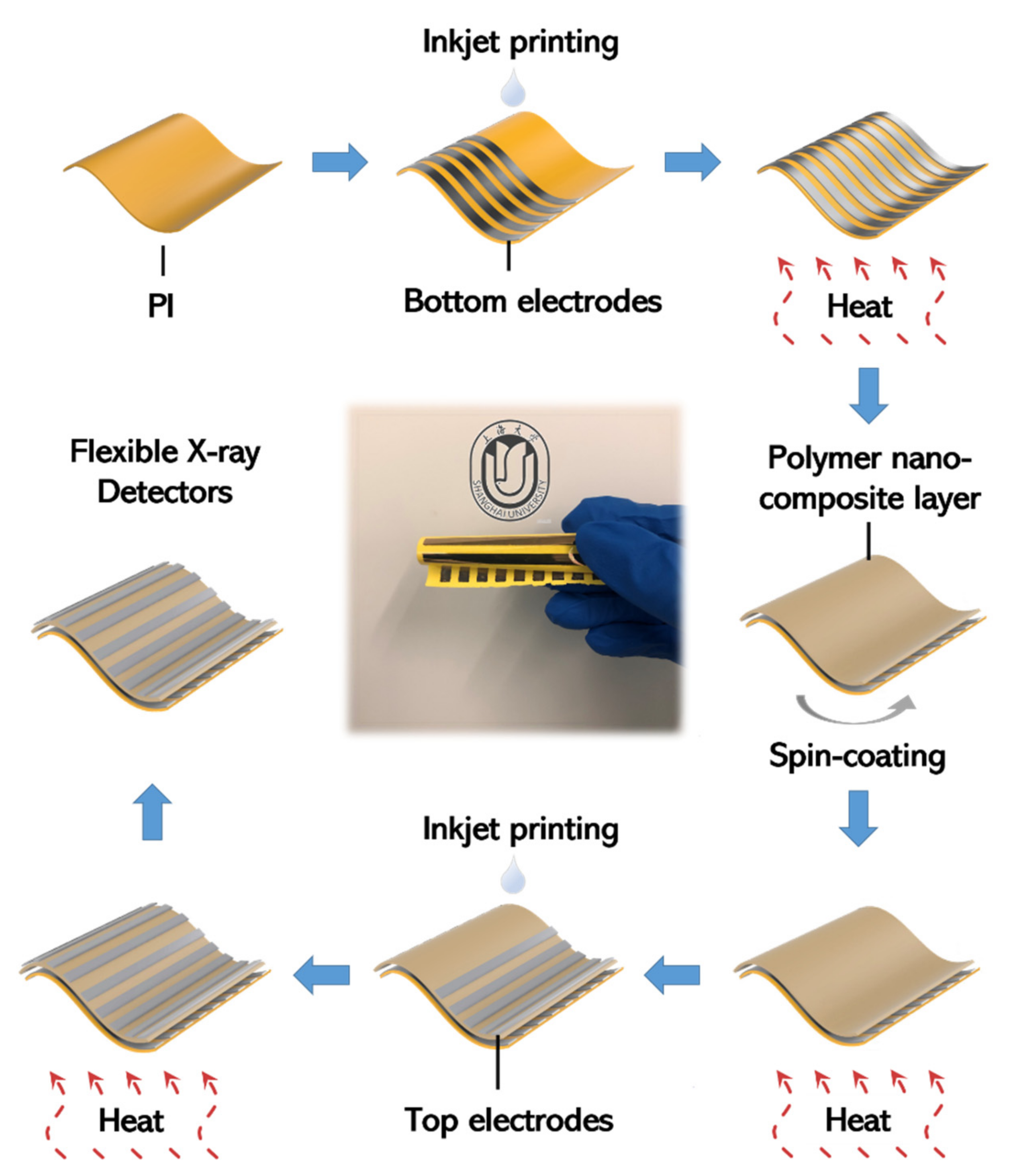
The schematic diagram of the device fabrication is shown in Figure 1, and the detail process is described as follows:
Bottom electrodes The PI was cleaned with deionized water for 10 min and dried with compressed air before using. The bottom electrodes were printed on the PI substrate. In the printing process, the substrate temperature was set at room temperature, and the Ag ink was jetted with a 30 μm dot pitch and only one nozzle was used during the printing process. Two layers were printed consecutively to ensure good continuity and conductivity of the printing electrodes. Then, the substrate was baked at 150 °C for 30 min. The square resistance of the bottom electrode was about 450 mΩ/cm2.
Polymer nanocomposite layer Different masses of Bi2O3 nanoparticles were added into the 2 g PDMS samples, respectively, and stirred for 5 min to obtain polymer nanocomposite slurries with different weight ratios (weight ratio %) of 10 (β-10%), 30 (β-30%), 50 (β-50%), 70 (β-70%), 90 (β-90%), and 110 (β-110%), respectively. The concentrations of Bi2O3 are listed in Table 1. The weight ratio used in this work is defined as:
Then, the polymer nanocomposite slurries were spin coated on the bottom electrodes and the samples were cured at 80 °C for 2 h.
Top electrodes The surface of the polymer nanocomposite layer was hydrophobic and could not provide suitable wettability for the Ag ink. In this study, we used an oxygen plasma treatment (250 W for 20 s) to modify the surface of the polymer nanocomposite layer to be hydrophilic. Then, the top electrodes were printed on the polymer nanocomposite layer with a 50 μm dot pitch and only one nozzle was used during the printing process. Two layers were printed consecutively to ensure good continuity and conductivity. Finally, the samples were baked at 150 °C for 30 min. The square resistance of the top electrode was about 750 mΩ/cm2.
2.3. Characterization
All the measurements were carried out in air at room temperature using an active device area of 0.09 cm2. A semiconductor Parameter Analyzer (PDA, FS-380, PSAIC, Beijing, China) was used to measure the current-voltage characteristics, with a tube X-ray beam (Moxtek MADPRO, MOXTEK, Orem, UT, USA) with accelerating voltage of 60 kV under a dose-rate range of 0.023–11.97 mGyair s−1. Dose calibration was completed using a radiation dosimeter (IBA, Magic MaX Universal, Wuhan, China) in a lead chamber. Inkjet printing was performed with a Fujifilm Dimatix DMP-2831 (FUJIFILM Dimatix Inc., Santa Clara, LA, USA), assembled with a 10 pL rated droplet volume ink cartridge with a 16-nozzle piezoelectric printhead. All printing processes were performed at a jetting frequency of 5 kHz. A planetary mixer (ZYMC-580, Shenzhen, China) was used to mix the Bi2O3 nanoparticles and PDMS.
The X-ray diffraction (XRD) was carried out on a Rigaku MinFlex 6G system (Tokyo, Japan). The scanning electron microscope (SEM) experiments were obtained using a ZEISS Sigma 300 (Jena, Germany). The transmission electron microscopy (TEM) images were obtained using a Tecnai G2 F20 (FEI, Hillsboro, OR, USA). The electronic differential system (EDS) analysis was carried out using an X-MaxN Oxford Instrument system (Oxford, UK). The thermogravimetric analysis (TGA) was carried out using a Mettler Toledo LF system (Zurich, Switzerland), in a temperature range of 25–650 °C under nitrogen atmosphere, at a heating rate of 10 °C/min.
3. Results and Discussion
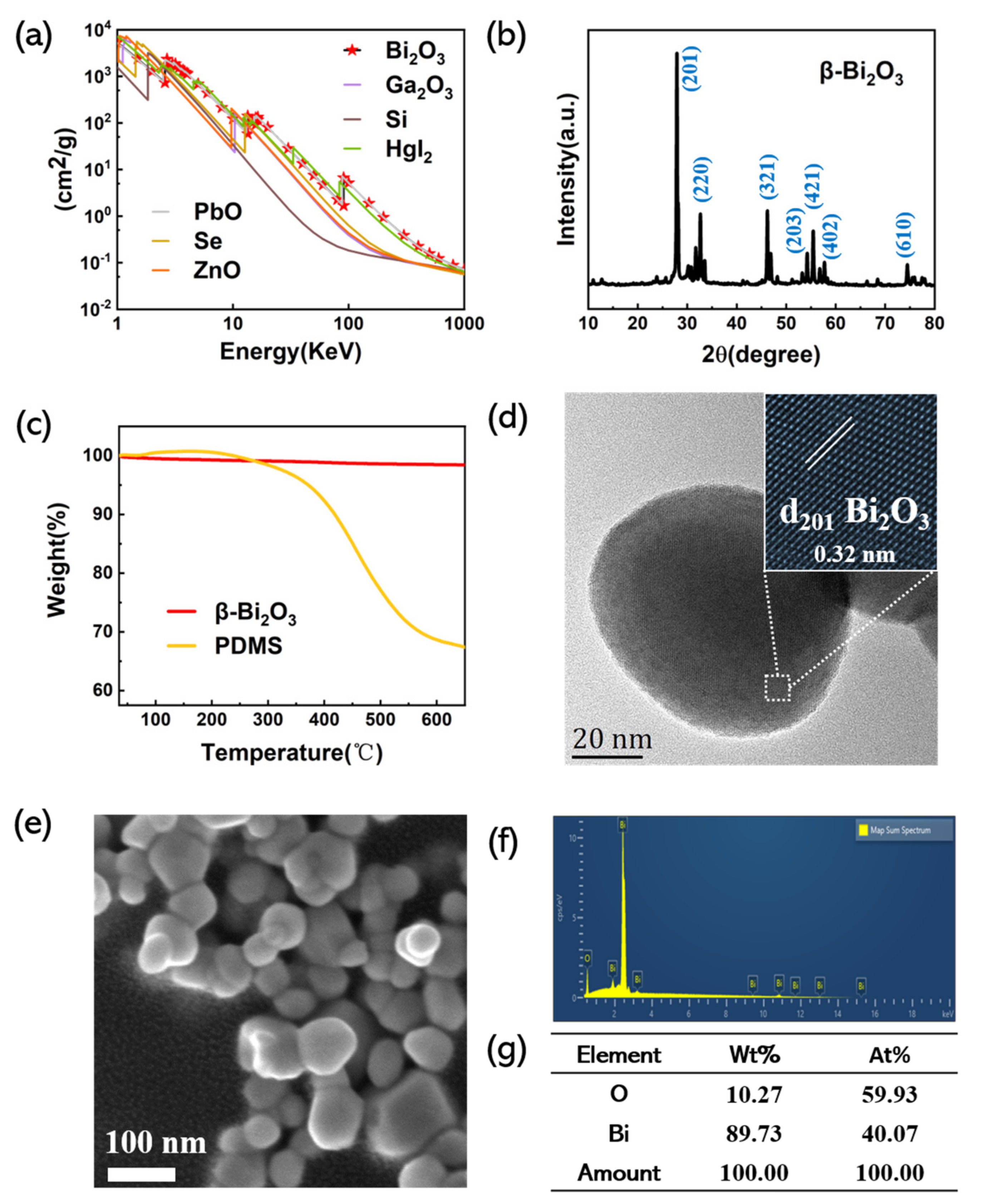
The linear attenuation coefficients of Bi2O3 and several typical semiconductors in the energy range of 1−1000 keV were calculated based on the data from the National Institute of Standards and Technology, as shown in Figure 2a. A typical XRD pattern of the sample is shown in Figure 2b and exhibits the characteristic diffraction peaks indexed to (201), (220), (321), (203), (421), (402), and (610). All observed XRD patterns match with the standard (JCPDS 27–0050) of pure β-Bi2O3 nanoparticles. Figure 2c shows the TGA of Bi2O3 nanoparticles and PDMS. The weight loss curve of PDMS shows a single step weight reduction of 38.2% between 341 and 566 °C. This was due to the loss of methyl groups on the Si-O backbone.The β-Bi2O3 nanoparticles have excellent thermal stability with almost no loss during the test. Figure 2d shows the TEM image of highly crystalline β-Bi2O3 nanoparticles. The high-resolution TEM reveals lattice fringes corresponding to the (201) plane of β-Bi2O3 (Figure 2d inset), in agreement with the XRD spectra. In Figure 2e, the SEM image provides an overall view of the β-Bi2O3 nanoparticles. An average size of ~40 nm can be observed for β-Bi2O3. Figure 2f,g is the EDS of β-Bi2O3 nanoparticles and indicates the element stoichiometric ratio of Bi and O is 2:3.
The X-ray detector developed in this work was based on PDMS and β-Bi2O3 nanoparticles. In order to optimize the detector’s performance, the concentration of β-Bi2O3 nanoparticles in the polymer nanocomposite layer was increased for increased X-ray attenuation (10, 30, 50, 70, 90, and 110 weight ratios %; X weight ratio % is noted as β-X%).
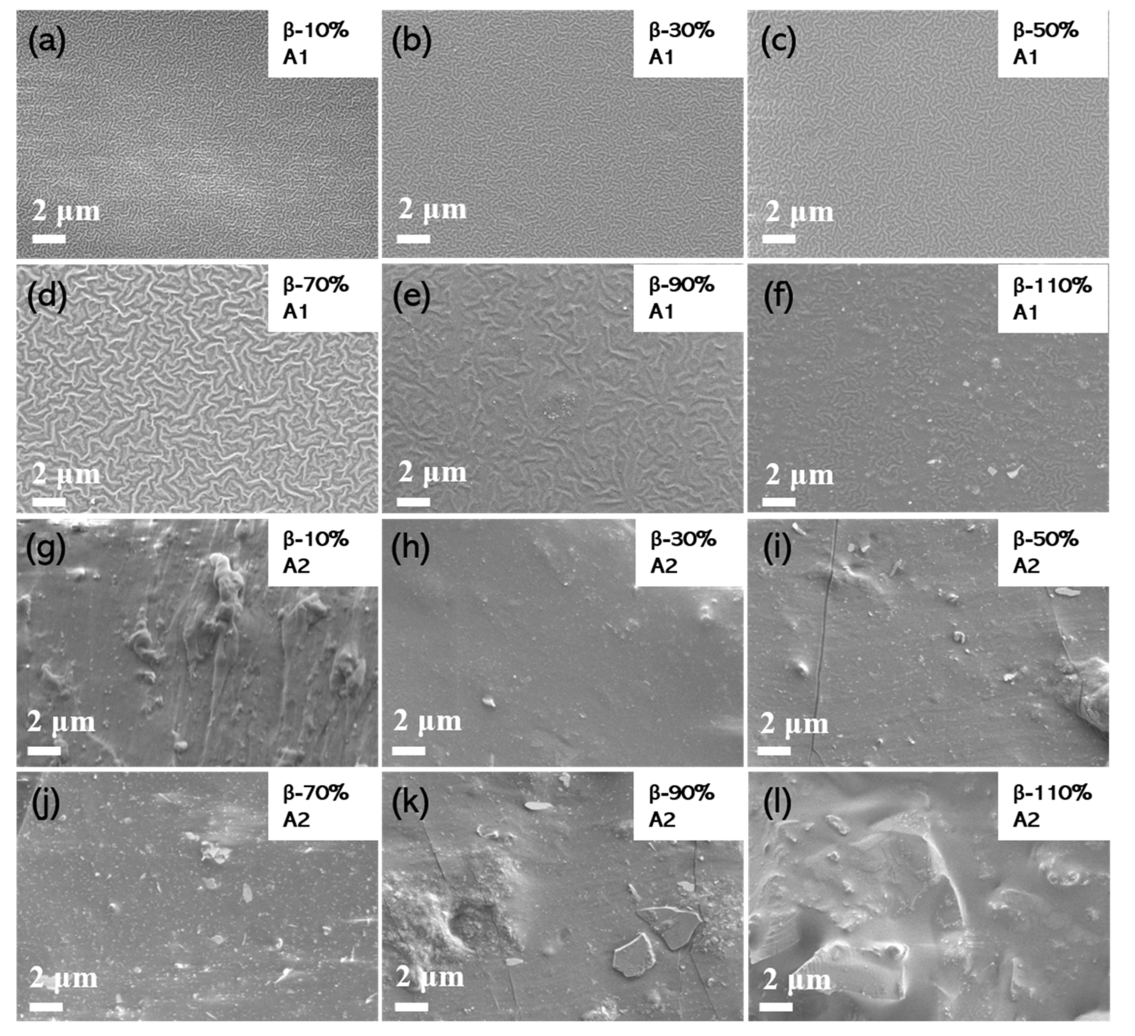
It is important to analyze the surface morphology of organic materials. From the micrographs, the nature of the surface, particle distribution, and surface failure can be observed. The surface microstructure and roughness can be easily studied by SEM, and the wettability of the surface is usually affected by the microstructure and roughness on the surface [44]. In Figure 3a–f, the SEM images demonstrate the surface morphology of the polymer nanocomposite layers as the weight percentage increases. It can clearly be seen that the surfaces of polymer nanocomposite layers changed from pleated to flat as the weight percentage increases. In Figure 3a, there are lots of wrinkles all over the surface. When the weight percentage increases to 110%, the surface morphology becomes flatter than the others. The difference in surface morphology may be attributed to the influence of the different doping contents of nanoparticles on the structure of PDMS [45]. In Figure 3g–l, the SEM images show the cross-section of the polymer nanocomposite films with different weight rates. As shown in Figure 3g–j, the β-Bi2O3 nanoparticles were evenly dispersed in the PDMS. However, the β-Bi2O3 nanoparticles in β-90% and β-110% were agglomerate (Figure 3k–l). This uneven material distribution may have a negative impact on the transfer of charges.
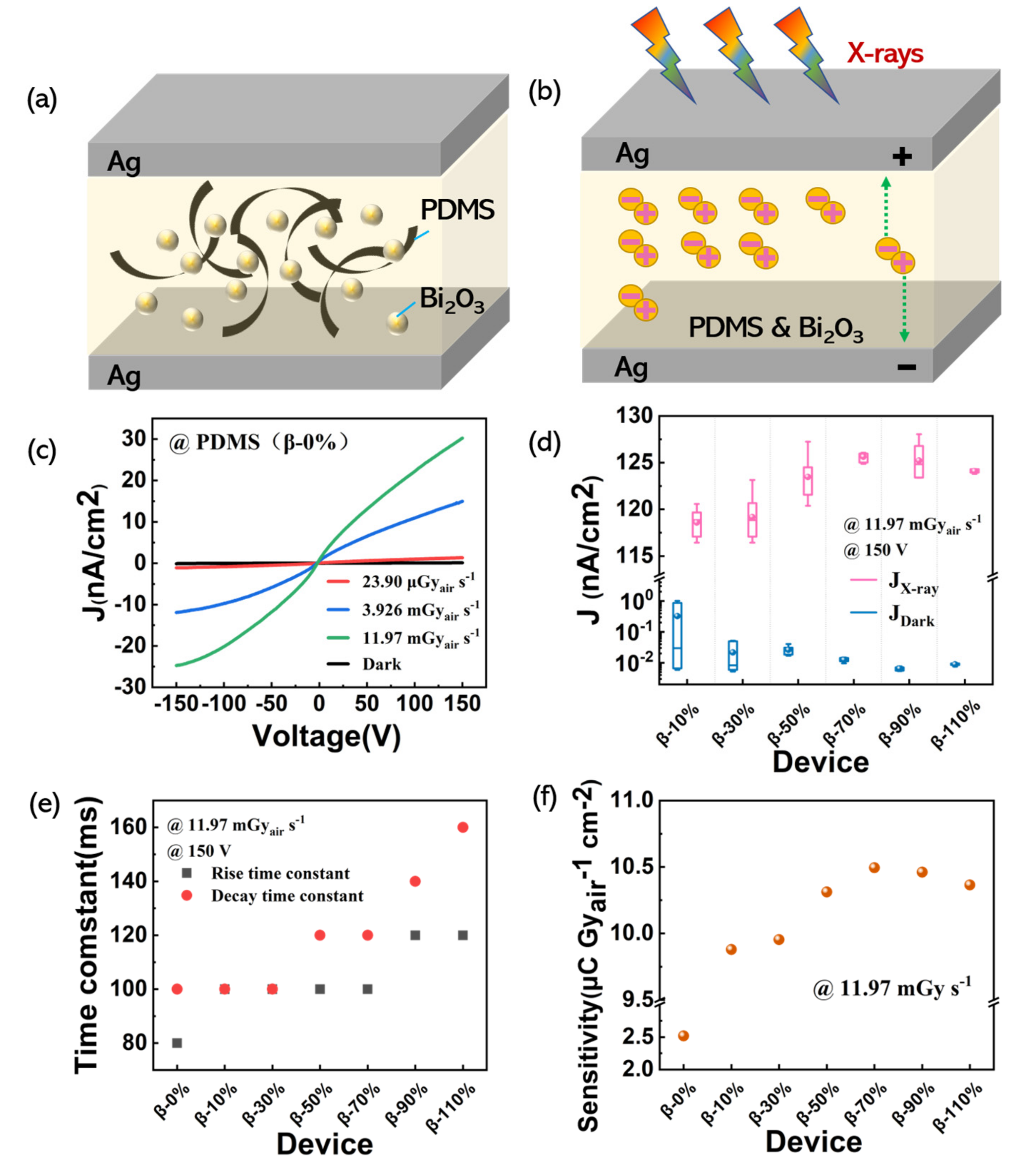
The schematic of the device structure is shown in Figure 4a. The polymer nanocomposite layer contains β-Bi2O3 nanoparticles and PDMS is sandwiched between two Ag electrodes. When the X-rays are irradiated, electrons and holes are generated in the polymer nanocomposite layer, and they move to the positive and negative electrodes, respectively, under the influence of the electric field to form a current (Figure 4b). To evaluate the performances of the devices, we expose detectors under an X-ray source to measure the electrical signal including the dark current density, X-ray current density and rise, and decay time constants in Figure 4c–f.
First, we explored the X-ray detection performance of pure PDMS. In Figure 4c, the X-ray current density of PDMS is exhibited under different dose rates of X-rays (from −150 to 150 V). In order to study the electrical properties of the detector under different weight ratios of β-Bi2O3 nanoparticles, we measured the photocurrent density and dark current density of the detector. Figure 4d shows the photocurrent density and dark current density of different devices. The box plot clearly shows that the photocurrent density begins to decrease after the β-70% device reaches the highest value as the content of nanoparticles increases. The dark current density starts to increase after the β-90% device reaches its minimum value. Figure 4e shows the rise time (to 90% of the maximum signal) and the decay time (to 10% of the maximum) as a function of the devices with different weight percentages. The slow response (>100 ms) is due to the trap states generally present in metal oxide surfaces which impede charge transfer [46].
The sensitivity (S) of a material is a key parameter for X-ray detectors because it can allow the material to easily detect a small X-ray dose or, in other words, it reduces ionizing radiation risks [17]. The definition of sensitivity is the linear dependence of the X-ray photocurrent signal as a function of impinging dose rate:
where and are the current under X-ray irradiation and in the dark, respectively, D is the dose rate, and V is the active detecting area.
The sensitivity of different devices under 11.97 mGyair s−1 at 150 V bias voltage are shown in Figure 4f. The sensitivity of pure PDMS is about 2.51 μC Gyair−1 cm−2. The highest sensitivity of the detectors with different β-Bi2O3 weight ratio is 10.49 μC Gyair−1 cm−2 (device β-70%) under 11.97 mGyair s−1 at 150 V bias voltage.
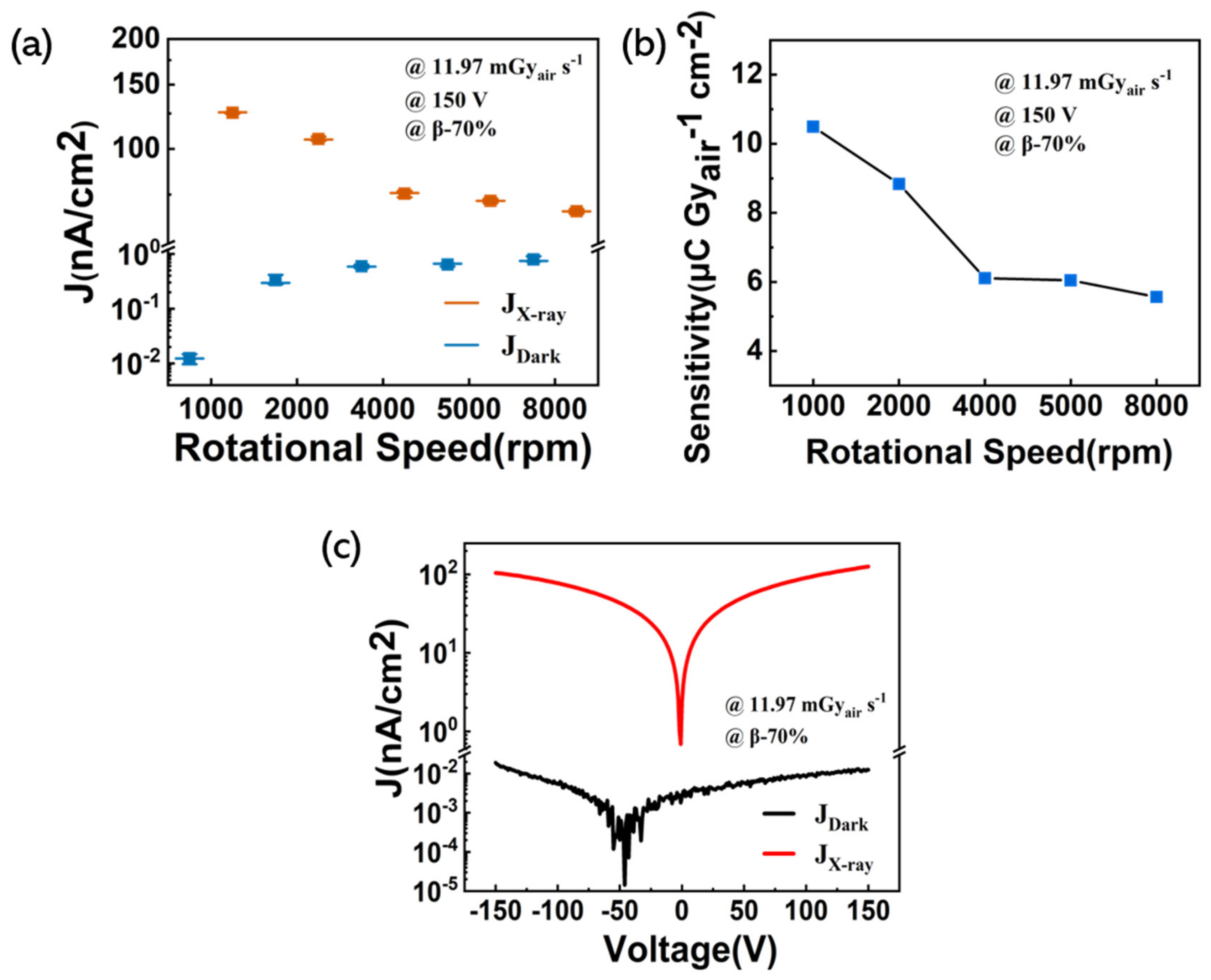
After the previous discussion, we found that the β-70% detector had the highest sensitivity among the devices with different nanoparticle contents. In order to further optimize the performance of the device, the thickness of the β-70% detector was varied by changing the spin coating rotational speed. Table 2 lists the thicknesses of the polymer nanocomposite layer at different speeds. Figure 5a shows the X-ray current density and dark current density of different thickness devices. The dark current density behavior is speculated based on the decreased resistance between the top and bottom electrodes as the rotational speed increases. The X-ray current density decreased as the thickness decreased. This may be due to a decrease in the number of charges generated by the polymer nanocomposite film under the same dose of X-ray radiation as the film thickness decreases.
Figure 5b shows the sensitivity as a function of the different thicknesses of devices. When a 290 µm thick (1000 rpm) polymer nanocomposite device was measured under 60 keV X-rays with a bias voltage of 150 V, the sensitivity was up to 10.49 µC Gyair−1 cm−2. Figure 5c shows the I−V characteristics of the β-70% detector (1000 rpm) under X-ray irradiation with a dose rate of 11.97 mGyair s−1. The JX-ray is 10,000-fold higher than the Jdark at 150 V bias voltage, indicating a high photo-to-dark current ratio of the detector.
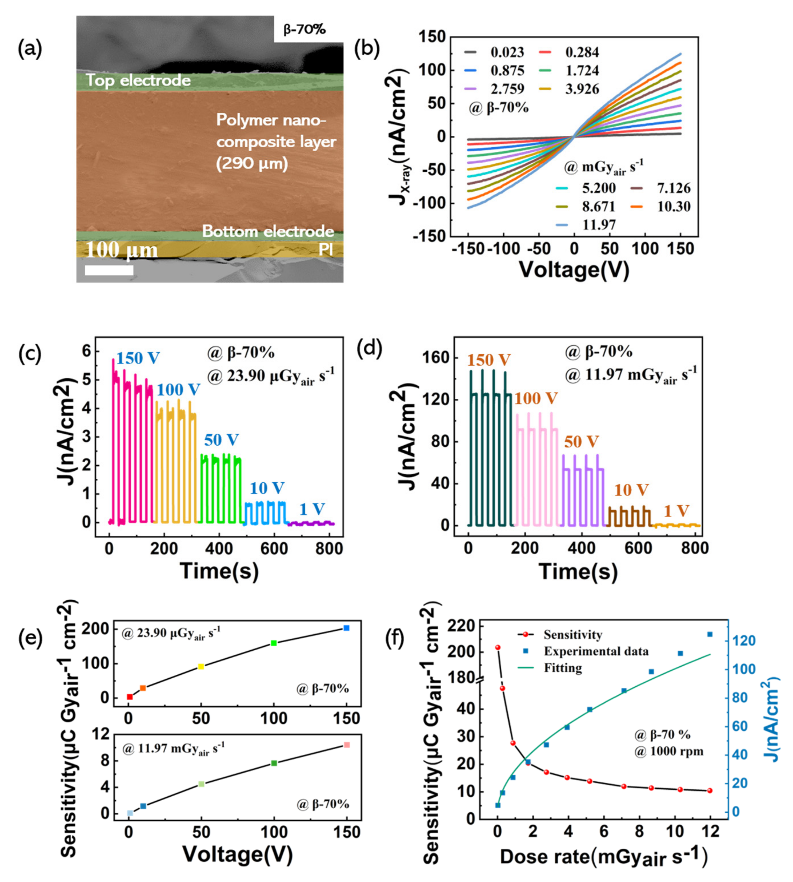
In Figure 6a, cross-sectional analysis by SEM shows the different layers of the detector. The β-70% polymer nanocomposite layer (1000 rpm) was evaluated in a device with a structure composed of PI (35 μm)/bottom electrode (20 μm)/polymer nanocomposite layer (290 μm)/top electrode (35 μm). Figure 6b shows the JX-ray of the detector under X-ray irradiation with the dose rate in the range of 0.023–11.97 mGyair s−1. It is obvious that all the JX-ray increase with the increasing X-ray dose rate. In Figure 6c,d, the transient response of the detector was measured as the X-ray tube was switched between on and off states with a dose rate of 11.97 μGyair s−1 and 23.90 mGyair s−1 at different bias voltages. No matter under different bias voltages or different dose rates, the detector exhibited a fast response and excellent repeatability. Figure 6e shows that the sensitivity increased monotonically with the increasing bias voltage. The X-ray generated charges can rapidly transport to the electrodes with a low recombination possibility at a high bias voltage, leading to enhanced carrier collection efficiency [47]. The sensitivity of the β-70% detector (1000 rpm) was increased to 203.58 μC Gyair−1 cm−2 under a dose rate of 23.90 μGyair s−1 at a 150 V bias voltage.
Figure 6f shows the dose rates as a function of the JX-ray and the sensitivity. Laura Basirico et al. proposed that the nonlinearity between the JX-ray and the dose rates may come from the photoconductive gain [48]. The radiation time determines the sensitivity of the organic X-ray detector, due to the existence of the photoconductive gain, i.e., the longer the exposure time, the sensitivity shows the maximum at low dose rates, and shows a nonlinear relationship with the increasing dose rate. During our test, we exposed our device to X-rays for more than 100 s to obtain the average X-ray current density. Thus, a sublinear relationship between the JX-ray and the increasing dose rate could clearly be observed. To evaluate the sensitivity of the β-70% detector (1000 rpm), the slope of the device output JX-ray versus X-ray dose rate was calculated. The highest experimental sensitivity was 203.58 μC Gyair−1 cm−2 and was obtained at a low dose rate of 23.90 μGyair s−1 and 150 V bias voltage. If we take the layer thickness into account, such as done in [17,49], the sensitivity value can be 702 μC Gyair−1 cm−3. We further compared the sensitivity value of our device with the detectors provided in the literature that had the same structure type as our device, as shown in Table 3. Our detector shows better sensitivity than similar types of devices in the literature, and it also provides a potential possibility for further exploration of flexible, non-toxic, and environmentally friendly X-ray detectors in the future.
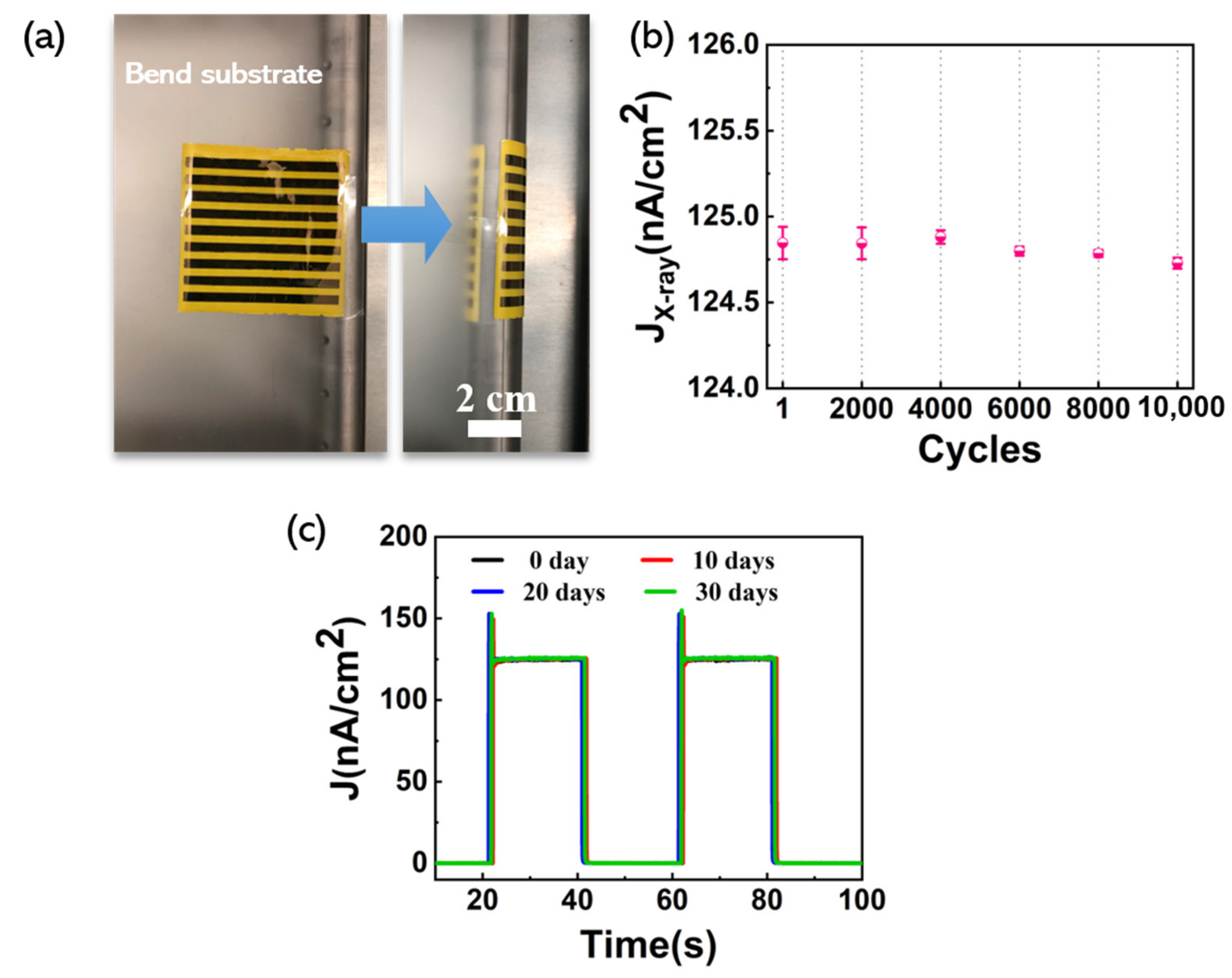
To evaluate the mechanical flexibility and stability of the β-70% detector (1000 rpm), we characterized the detectors in a curly configuration, and we also re-tested the time-dependent response performance every 10 days. Figure 7a shows the experimental set-up for testing the flexibility of the devices, and the bending radius is set to 1 cm. The detector array was pasted on the bending substrate and curled onto the surface of the metal rod by mechanical movement. In Figure 7b, it shows the JX-ray measured under a dose rate of 11.97 mGyair s−1 at 150 V bias voltage after curling and as a function of the number of curling cycles applied to the devices. The error bars refer to the fluctuation of the signal amplitude of the devices. It can be clearly seen that the JX-ray decreases slightly with an increase in the number of curling cycles. Figure 7c shows the stability of the detector stored in air. We repeatedly measured the time-dependent response performance of the device four times in one month. Three on/off switching cycles (20 s for each state) of the X-ray in the same condition were tested, and we extracted the last two cycles to assess the stability. In these numerous tests, there was almost no change found in the J.
4. Conclusions
In conclusion, a flexible direct X-ray detector based on Bi2O3 nanoparticles in PDMS with high sensitivity was successfully investigated. We discussed the performance of polymer nanocomposite layers with different contents of Bi2O3 NPs and optimized the thickness to obtain the optimal X-ray detector (β-70% detector, 1000 rpm). The device has a consistent response at different dose rates, and the JX-ray is 10,000-fold higher than the Jdark at a 150 V bias voltage, which proves that the device has excellent detection performance. The highest sensitivity (203.58 μC Gyair−1 cm−2 in β-70% detector) was achieved under a dose rate of 23.90 μGyair s−1 at 150 V bias voltage. Additionally, no significant degradation was observed during the bending and stability test. These results provided guidance for the next-generation high-performance flexible direct X-ray detectors.
Author Contributions
Conceptualization, L.M. and Y.L.; methodology, Y.L.; software, L.M.; validation, L.M., L.Y. and Y.L.; formal analysis, L.M. and Y.L.; investigation, L.M.; resources, L.Y.; data curation, H.C.; writing—original draft preparation, L.M. and Y.L.; writing—review and editing, L.M. and Y.L.; visualization, L.M. and Y.L.; supervision, J.Z.; project administration, Y.L.; funding acquisition, J.Z. All authors have read and agreed to the published version of the manuscript.
Funding
This research was funded by the National Natural Science Foundation of China (51725505), the National key research and development program of China (2017YFB0404703), the Shanghai Industrial foundation project (GYQJ-2018-2-04), and the Shanghai Science and Technology Funds (17DZ1930502).
Institutional Review Board Statement
Not applicable.
Informed Consent Statement
Not applicable.
Data Availability Statement
The data presented in this study are available on request from the corresponding author.
Conflicts of Interest
The authors declare no conflict of interest.
References
- Xu, Q.; Wang, X.; Zhang, H.; Shao, W.; Nie, J.; Guo, Y.; Wang, J.; Ouyang, X. CsPbBr3 Single Crystal X-ray Detector with Schottky Barrier for X-ray Imaging Application. ACS Appl. Electron. Mater. 2020, 2, 879–884. [Google Scholar] [CrossRef]
- Nambiar, S.; Osei, E.K.; Yeow, J.T.W. Polymer nanocomposite-based shielding against diagnostic X-rays. J. Appl. Polym. Sci. 2013, 127, 4939–4946. [Google Scholar] [CrossRef]
- Sakdinawat, A.; Attwood, D. Nanoscale X-ray imaging. Nat. Photonics 2010, 4, 840–848. [Google Scholar] [CrossRef]
- Szeles, C. CdZnTe and CdTe materials for X-ray and gamma ray radiation detector applications. Phys. Status Solidi b 2004, 241, 783–790. [Google Scholar] [CrossRef]
- Kasap, S.; Frey, J.B.; Belev, G.; Tousignant, O.; Mani, H.; Greenspan, J.; Laperriere, L.; Bubon, O.; Reznik, A.; DeCrescenzo, G.; et al. Amorphous and polycrystalline photoconductors for direct conversion flat panel X-ray image sensors. Sensors 2011, 11, 5112–5157. [Google Scholar] [CrossRef] [Green Version]
- Kasap, S.O.; Rowlands, J.A. Review X-ray photoconductors and stabilized a-Se for direct conversion digital flat-panel X-ray image-detectors. J. Mater. Sci. Mater. Electron. 2000, 11, 179–198. [Google Scholar] [CrossRef]
- Owens, A.; Peacock, A. Compound semiconductor radiation detectors. Nucl. Instrum. Methods A 2004, 531, 18–37. [Google Scholar] [CrossRef]
- Yakunin, S.; Sytnyk, M.; Kriegner, D.; Shrestha, S.; Richter, M.; Matt, G.J.; Azimi, H.; Brabec, C.J.; Stangl, J.; Kovalenko, M.V.; et al. Detection of X-ray photons by solution-processed organic-inorganic perovskites. Nat. Photonics 2015, 9, 444–449. [Google Scholar] [CrossRef] [PubMed]
- Morimune, T.; Kajii, H.; Ohmori, Y. Photoresponse Properties of a High-Speed Organic Photodetector Based on Copper–Phthalocyanine Under Red Light Illumination. IEEE Photon. Technol. Lett. 2006, 18, 2662–2664. [Google Scholar] [CrossRef]
- Cowan, S.R.; Wang, J.; Yi, J.; Lee, Y.J.; Olson, D.C.; Hsu, J.W. Intensity and wavelength dependence of bimolecular recombination in P3HT: PCBM solar cells. J. Appl. Phys. 2013, 113, 154504. [Google Scholar] [CrossRef]
- Büchele, P.; Morana, M.; Bagnis, D.; Tedde, S.F.; Hartmann, D.; Fischer, R.; Schmidt, O. Space charge region effects in bidirectional illuminated P3HT:PCBM bulk heterojunction photodetectors. Org. Electron. 2015, 22, 29–34. [Google Scholar] [CrossRef]
- Wei, S.; Yang, M.; Sun, H.; Li, F.; Xiao, F.; Zou, J.; Ren, A.; Huang, Y.; Xiong, Z.; Yuan, L.; et al. Single Crystal CdSe X-ray Detectors with Ultra-High Sensitivity and Low Detection Limit. ACS Appl. Mater. Interfaces 2020. [Google Scholar] [CrossRef] [PubMed]
- Zhang, H.; Wang, F.; Lu, Y.; Sun, Q.; Xu, Y.; Zhang, B.-B.; Jie, W.; Kanatzidis, M.G. High-sensitivity X-ray detectors based on solution-grown caesium lead bromide single crystals. J. Mater. Chem. C 2020, 8, 1248–1256. [Google Scholar] [CrossRef]
- Intaniwet, A.; Mills, C.A.; Shkunov, M.; Sellin, P.J.; Keddie, J.L. Heavy metallic oxide nanoparticles for enhanced sensitivity in semiconducting polymer X-ray detectors. Nanotechnology 2012, 23, 235502. [Google Scholar] [CrossRef] [PubMed] [Green Version]
- Mills, C.A.; Al-Otaibi, H.; Intaniwet, A.; Shkunov, M.; Pani, S.; Keddie, J.L.; Sellin, P.J. Enhanced X-ray detection sensitivity in semiconducting polymer diodes containing metallic nanoparticles. J. Phys. D Appl. Phys. 2013, 46, 275102. [Google Scholar] [CrossRef] [Green Version]
- Demchyshyn, S.; Verdi, M.; Basirico, L.; Ciavatti, A.; Hailegnaw, B.; Cavalcoli, D.; Scharber, M.C.; Sariciftci, N.S.; Kaltenbrunner, M.; Fraboni, B. Designing Ultraflexible Perovskite X-ray Detectors through Interface Engineering. Adv. Sci. 2020, 7, 2002586. [Google Scholar] [CrossRef]
- Thirimanne, H.M.; Jayawardena, K.; Parnell, A.J.; Bandara, R.M.I.; Karalasingam, A.; Pani, S.; Huerdler, J.E.; Lidzey, D.G.; Tedde, S.F.; Nisbet, A.; et al. High sensitivity organic inorganic hybrid X-ray detectors with direct transduction and broadband response. Nat. Commun. 2018, 9, 2926. [Google Scholar] [CrossRef]
- Jayawardena, K.; Thirimanne, H.M.; Tedde, S.F.; Huerdler, J.E.; Parnell, A.J.; Bandara, R.M.I.; Mills, C.A.; Silva, S.R.P. Millimeter-Scale Unipolar Transport in High Sensitivity Organic-Inorganic Semiconductor X-ray Detectors. ACS Nano 2019, 13, 6973–6981. [Google Scholar] [CrossRef]
- Ciavatti, A.; Cramer, T.; Carroli, M.; Basiricò, L.; Fuhrer, R.; De Leeuw, D.M.; Fraboni, B. Dynamics of direct X-ray detection processes in high-Z Bi2O3 nanoparticles-loaded PFO polymer-based diodes. Appl. Phys. Lett. 2017, 111, 183301. [Google Scholar] [CrossRef] [Green Version]
- Zhang, Z.; Yang, G. Recent advancements in using perovskite single crystals for gamma-ray detection. J. Mater. Sci. Mater. Electron. 2020. [Google Scholar] [CrossRef]
- Simon, M.; Ford, R.A.; Franklin, A.R.; Grabowski, S.P.; Menser, B.; Much, G.; Nascetti, A.; Overdick, M.; Powell, M.J.; Wiechert, D.U. Analysis of lead oxide (PbO) layers for direct conversion X-ray detection. IEEE Trans. Nucl. Sci. 2005, 52, 2035–2040. [Google Scholar] [CrossRef]
- Shrestha, S.; Fischer, R.; Matt, G.J.; Feldner, P.; Michel, T.; Osvet, A.; Levchuk, I.; Merle, B.; Golkar, S.; Chen, H.; et al. High-performance direct conversion X-ray detectors based on sintered hybrid lead triiodide perovskite wafers. Nat. Photonics 2017, 11, 436–440. [Google Scholar] [CrossRef]
- Qamar, A.; LeBlanc, K.; Semeniuk, O.; Reznik, A.; Lin, J.; Pan, Y.; Moewes, A. X-ray spectroscopic study of amorphous and polycrystalline PbO films, alpha-PbO, and beta-PbO for direct conversion imaging. Sci. Rep. 2017, 7, 13159. [Google Scholar] [CrossRef]
- Wei, H.; Fang, Y.; Mulligan, P.; Chuirazzi, W.; Fang, H.-H.; Wang, C.; Ecker, B.R.; Gao, Y.; Loi, M.A.; Cao, L.; et al. Sensitive X-ray detectors made of methylammonium lead tribromide perovskite single crystals. Nat. Photonics 2016, 10, 333–339. [Google Scholar] [CrossRef]
- Pan, W.; Wu, H.; Luo, J.; Deng, Z.; Ge, C.; Chen, C.; Jiang, X.; Yin, W.-J.; Niu, G.; Zhu, L.; et al. Cs2AgBiBr6 single-crystal X-ray detectors with a low detection limit. Nat. Photonics 2017, 11, 726–732. [Google Scholar] [CrossRef]
- Hiyama, F.; Noguchi, T.; Koshimizu, M.; Kishimoto, S.; Haruki, R.; Nishikido, F.; Fujimoto, Y.; Aida, T.; Takami, S.; Adschiri, T.; et al. X-ray detection properties of plastic scintillators containing surface-modified Bi2O3 nanoparticles. Jpn. J. Appl. Phys. 2018, 57, 052203. [Google Scholar] [CrossRef]
- Yao, L.; Niu, G.; Yin, L.; Du, X.; Lin, Y.; Den, X.; Zhang, J.; Tang, J. Bismuth halide perovskite derivatives for direct X-ray detection. J. Mater. Chem. C 2020, 8, 1239–1243. [Google Scholar] [CrossRef]
- Jagdale, P.; Rovere, M.; Ronca, R.; Vigneri, C.; Bernardini, F.; Calzetta, G.; Tagliaferro, A. Determination of the X-ray attenuation coefficient of bismuth oxychloride nanoplates in polydimethylsiloxane. J. Mater. Sci. 2020, 55, 7095–7105. [Google Scholar] [CrossRef]
- Praveenkumar, P.; Venkatasubbu, G.D.; Thangadurai, P.; Prakash, T. Nanocrystalline bismuth oxyiodides thick films for X-ray detector. Mat. Sci. Semicon. Proc. 2019, 104, 104686. [Google Scholar] [CrossRef]
- Shamaila, S.; Sajjad, A.K.L.; Chen, F.; Zhang, J. Study on highly visible light active Bi2O3 loaded ordered mesoporous titania. Appl. Catal. B 2010, 94, 272–280. [Google Scholar] [CrossRef]
- Jayakumar, S.; Saravanan, T.; Philip, J. Thermal Stability and X-ray Attenuation Studies on alpha-Bi2O3, beta-Bi2O3 and Bi Based Nanocomposites for Radiopaque Fabrics. J. Nanosci. Nanotechnol. 2018, 18, 3969–3981. [Google Scholar] [CrossRef]
- Keum, C.; Murawski, C.; Archer, E.; Kwon, S.; Mischok, A.; Gather, M.C. A substrateless, flexible, and water-resistant organic light-emitting diode. Nat. Commun. 2020, 11, 6250. [Google Scholar] [CrossRef] [PubMed]
- Zhang, Z.; Chen, L.; Yang, X.; Li, T.; Chen, X.; Li, X.; Zhao, T.; Zhang, J. Enhanced Flexible Piezoelectric Sensor by the Integration of P(VDF-TrFE)/AgNWs Film With a-IGZO TFT. IEEE Electron Device Lett. 2018. [Google Scholar] [CrossRef]
- Liu, Y.; Sun, N.; Liu, J.; Wen, Z.; Sun, X.; Lee, S.T.; Sun, B. Integrating a Silicon Solar Cell with a Triboelectric Nanogenerator via a Mutual Electrode for Harvesting Energy from Sunlight and Raindrops. ACS Nano 2018, 12, 2893–2899. [Google Scholar] [CrossRef]
- Qiu, Q.; Chen, H.; You, Z.; Feng, Y.; Wang, X.; Wang, Y.; Ying, Y. Shear Exfoliated Metal-Organic Framework Nanosheet-Enabled Flexible Sensor for Real-Time Monitoring of Superoxide Anion. ACS Appl. Mater. Interfaces 2020, 12, 5429–5436. [Google Scholar] [CrossRef]
- Cramer, T.; Sacchetti, A.; Lobato, M.T.; Pedro, B.; Vincent, F.; Mohamed, B.; Jacquelin, B.; Elvira, F.; Rodrigo, M.; Beatrice, F. Radiation-Tolerant Flexible Large-Area Electronics Based on Oxide Semiconductors. Adv. Electron. Mater. 2016, 2, 1500489. [Google Scholar] [CrossRef]
- Cramer, T.; Fratelli, I.; Barquinha, P.; Ann, S.; Cristina, F.; Frank, D.; Christophe, L.; Rodrigo, M.; Elvira, F.; Beatric, F. Passive radiofrequency X-ray dosimeter tag based on flexible radiation-sensitive oxide field-effect transistor. Sci. Adv. 2018, 46, eaat1825. [Google Scholar] [CrossRef] [Green Version]
- Ouyang, W.; Chen, J.; He, J.H.; Fang, X. Improved Photoelectric Performance of UV Photodetector Based on ZnO Nanoparticle-Decorated BiOCl Nanosheet Arrays onto PDMS Substrate: The Heterojunction and Ti3C2Tx MXene Conduction Layer. Adv. Electron. Mater. 2020, 6, 2000168. [Google Scholar] [CrossRef]
- Sabri, F.; Sebelik, M.E.; Meacham, R.; Boughter, J.D., Jr.; Challis, M.J.; Leventis, N. In vivo ultrasonic detection of polyurea crosslinked silica aerogel implants. PLoS ONE 2013, 8, e66348. [Google Scholar] [CrossRef] [Green Version]
- Allison, S.W.; Baker, E.S.; Lynch, K.J.; Sabri, F. In Vivo X-ray Imaging of Phosphor-Doped PDMS and Phosphor-Doped Aerogel Biomaterials. Int. J. Polym. Mater. Polym. Biomater. 2015, 64, 823–830. [Google Scholar] [CrossRef]
- Massaro, A.; Spano, F.; Cingolani, R.; Athanassiou, A. Experimental Optical Characterization and Polymeric Layouts of Gold PDMS Nanocomposite Sensor for Liquid Detection. IEEE Sens. J. 2011, 11, 1780–1786. [Google Scholar] [CrossRef]
- Wang, X.; Yang, B.; Liu, J.; Zhu, Y.; Yang, C.; He, Q. A flexible triboelectric-piezoelectric hybrid nanogenerator based on P(VDF-TrFE) nanofibers and PDMS/MWCNT for wearable devices. Sci. Rep. 2016, 6. [Google Scholar] [CrossRef] [Green Version]
- Sriphan, S.; Charoonsuk, T.; Maluangnont, T.; Vittayakorn, N. High-Performance Hybridized Composited-Based Piezoelectric and Triboelectric Nanogenerators Based on BaTiO3/PDMS Composite Film Modified with Ti0.8O2 Nanosheets and Silver Nanopowders Cofillers. ACS Appl. Energy Mater. 2019, 2, 3840–3850. [Google Scholar] [CrossRef]
- Ammar, S.; Ramesh, K.; Vengadaesvaran, B.; Ramesh, S.; Arof, A.K. Amelioration of anticorrosion and hydrophobic properties of epoxy/PDMS composite coatings containing nano ZnO particles. Prog. Org. Coat. 2016, 92, 54–65. [Google Scholar] [CrossRef]
- Xie, J.; Hu, J.; Lin, X.; Fang, L.; Wu, F.; Liao, X.; Luo, H.; Shi, L. Robust and anti-corrosive PDMS/SiO2 superhydrophobic coatings fabricated on magnesium alloys with different-sized SiO2 nanoparticles. Appl. Surf. Sci. 2018, 457, 870–880. [Google Scholar] [CrossRef]
- Kim, Y.H.; Sachse, C.; Machala, M.L.; May, C.; Müller-Meskamp, L.; Leo, K. Highly Conductive PEDOT:PSS Electrode with Optimized Solvent and Thermal Post-Treatment for ITO-Free Organic Solar Cells. Adv. Funct. Mater. 2011, 21, 1076–1081. [Google Scholar] [CrossRef]
- Kang, J.; Sangwan, V.K.; Lee, H.-S.; Liu, X.; Hersam, M.C. Solution-Processed Layered Gallium Telluride Thin-Film Photodetectors. ACS Photonics 2018. [Google Scholar] [CrossRef]
- Basirico, L.; Ciavatti, A.; Cramer, T.; Cosseddu, P.; Bonfiglio, A.; Fraboni, B. Direct X-ray photoconversion in flexible organic thin film devices operated below 1 V. Nat. Commun. 2016, 7, 13063. [Google Scholar] [CrossRef] [Green Version]
- Liang, H.; Cui, S.; Su, R.; Guan, P.; He, Y.; Yang, L.; Chen, L.; Zhang, Y.; Mei, Z.; Du, X. Flexible X-ray Detectors Based on Amorphous Ga2O3 Thin Films. ACS Photonics 2018, 6, 351–359. [Google Scholar] [CrossRef]
- Liu, J.; Shabbir, B.; Wang, C.; Wan, T.; Ou, Q.; Yu, P.; Tadich, A.; Jiao, X.; Chu, D.; Qi, D.; et al. Flexible, Printable Soft-X-ray Detectors Based on All-Inorganic Perovskite Quantum Dots. Adv. Mater. 2019, 31, e1901644. [Google Scholar] [CrossRef]
- Chen, J.; Tang, H.; Liu, B.; Zhu, Z.; Gu, M.; Zhang, Z.; Xu, Q.; Xu, J.; Zhou, L.; Chen, L.; et al. High-Performance X-ray Detector Based on Single-Crystal beta-Ga2O3:Mg. ACS Appl. Mater. Interfaces 2021. [Google Scholar] [CrossRef]
- Lai, S.; Cosseddu, P.; Basiricò, L.; Ciavatti, A.; Fraboni, B.; Bonfiglio, A. A Highly Sensitive, Direct X-ray Detector Based on a Low-Voltage Organic Field-Effect Transistor. Adv. Electron. Mater. 2017, 3, 1600409. [Google Scholar] [CrossRef]
Figure 1.
The schematic diagram of the device fabrication.

Figure 2.
(a) Absorption coefficients values of Bi2O3, Ga2O3, Si, HgI2, PbO, Se, and ZnO; (b) the XRD pattern; (c) the TGA of Bi2O3 nanoparticles and PDMS; (d) a TEM image of Bi2O3 nanoparticles, inset is high-resolution TEM image and shows the d-spacing of 0.32 nm correlating to the (201) plane; (e) a SEM image of Bi2O3 nanoparticles; (f,g) the EDS of Bi2O3 nanoparticles.

Figure 3.
SEM images of polymer nanocomposite layers with different weight percentages. (a–f) The surface of polymer nanocomposite layers with different weight percentages. (g–l) The cross-section of polymer nanocomposite layers with different weight percentages. A1 and A2 mean the surface and cross-section of the layers, respectively.

Figure 4.
(a) The schematic of the device structure; (b) a diagram of the process of the conductivity induced by X-ray exposure of the detector; (c) the I-V curve of PDMS under different dose rates; (d) the X-ray and dark current density box plot of different devices and the error bars represent the range of the current density values; (e) rise and decay time constants for detectors with increasing β-Bi2O3 nanoparticle loadings; (f) the sensitivity values for seven devices at 150 V bias voltage.

Figure 5.
(a) The X-ray and dark current density of device β-70% with different thicknesses; (b) the sensitivity of device β-70% with different thicknesses; (c) I−V characteristics of the β-70% detector (1000 rpm) in the dark and under X-ray irradiation on a logarithmic scale.
Figure 5.
(a) The X-ray and dark current density of device β-70% with different thicknesses; (b) the sensitivity of device β-70% with different thicknesses; (c) I−V characteristics of the β-70% detector (1000 rpm) in the dark and under X-ray irradiation on a logarithmic scale.

Figure 6.
The performance of the β-70% detector (1000 rpm): (a) The cross-section SEM image; (b) J−V curves of the detector under X-ray irradiation with different dose rates; (c,d) transient response of the detectors under X-ray irradiation with different dose rates; (e) the sensitivity of the detector at different bias voltages; (f) the sensitivity and X-ray current density of the detector at different dose rates with 150 V bias voltage.

Figure 7.
(a) Experimental set-up for testing the flexibility of the devices (bending radius is 1 cm); (b) JX-ray of the devices measured after 1, 2000, 4000, 6000, 8000, and 10,000 curling cycles; (c) time-dependent J of the detector measured every 10 days. The data displayed in Figure 7 was measured under a dose rate of 11.97 mGyair s−1 at 150 V bias voltage and in flat-substrate condition.


Table 1.
Concentrations of Bi2O3.
| Sample Name | Bi2O3 in the Dry Film | |
|---|---|---|
| Weight Ratio % | Weight Percent % | |
| β-10% | 10 | 9.1 |
| β-30% | 30 | 23.1 |
| β-50% | 50 | 33.3 |
| β-70% | 70 | 41.2 |
| β-90% | 90 | 47.4 |
| β-110% | 110 | 52.4 |
Table 2.
Correspondence between spin coating speed and thickness.
| Rotational Speed (rpm) | 1000 | 2000 | 4000 | 5000 | 8000 |
| Thickness (μm) | 290 | 100 | 52 | 40 | 16 |
Table 3.
The performances of the X-ray detector in this study as compared with similar detectors reported in the literature.
Table 3.
The performances of the X-ray detector in this study as compared with similar detectors reported in the literature.
| Materials | Sensitivity (μC Gyair−1 cm−2) | Voltage (V) | Thickness (μm) | Dose Rate 1 (μGyair s−1) | Reference |
|---|---|---|---|---|---|
| CsPbBr | 17.7 | 0.1 | 1000 | 17.2 | [50] |
| a-Se | 20 | 2000 | 200 | - | [9] |
| β-Ga2O3 | 66 | −15 | 400 | 695 | [51] |
| PTAA:Bi2O3 NPs | 0.4 2 | −200 | 20 | 13,000 | [14] |
| TIPS-pentacence | 4.8 | −3 | 0.1 | 6500 | [52] |
| PFO:Bi2O3 NPs | 24 | −80 | 1 | 20,000 | [19] |
| PDMS:Bi2O3 NPs | 203.58 | 150 | 290 | 23.90 | this work |
1 The minimum dose rate used when testing the device in the article. 2 Not mentioned in the article, estimated based on existing data.
Publisher’s Note: MDPI stays neutral with regard to jurisdictional claims in published maps and institutional affiliations. |
© 2021 by the authors. Licensee MDPI, Basel, Switzerland. This article is an open access article distributed under the terms and conditions of the Creative Commons Attribution (CC BY) license (https://creativecommons.org/licenses/by/4.0/).
Share and Cite
MDPI and ACS Style
Mao, L.; Li, Y.; Chen, H.; Yu, L.; Zhang, J. A High-Sensitivity Flexible Direct X-ray Detector Based on Bi2O3/PDMS Nanocomposite Thin Film. Nanomaterials 2021, 11, 1832. https://doi.org/10.3390/nano11071832
AMA Style
Mao L, Li Y, Chen H, Yu L, Zhang J. A High-Sensitivity Flexible Direct X-ray Detector Based on Bi2O3/PDMS Nanocomposite Thin Film. Nanomaterials. 2021; 11(7):1832. https://doi.org/10.3390/nano11071832
Chicago/Turabian StyleMao, Longmei, Yi Li, Hu Chen, Longxin Yu, and Jianhua Zhang. 2021. "A High-Sensitivity Flexible Direct X-ray Detector Based on Bi2O3/PDMS Nanocomposite Thin Film" Nanomaterials 11, no. 7: 1832. https://doi.org/10.3390/nano11071832
Note that from the first issue of 2016, this journal uses article numbers instead of page numbers. See further details here.