Article

MOS Capacitance Measurements for PEALD TiO2 Dielectric Films Grown under Different Conditions and the Impact of Al2O3 Partial-Monolayer Insertion

1
i3N, Departamento de Física, Universidade de Aveiro, Campus Universitário de Santiago, 3810-193 Aveiro, Portugal
2
Laboratório de Sistemas Integráveis, Escola Politécnica da Universidade de São Paulo (USP-SP), 05508-010 São Paulo, Brazil
3
Laboratório de Plasmas e Processos (LPP), Instituto Tecnológico de Aeronáutica (ITA), 12228-900 São José dos Campos, Brazil
4
Instituto de Ciência e Tecnologia, Universidade Federal de São Paulo, 12231-280 São José dos Campos, Brazil
5
Instituto Científico e Tecnológico, Universidade Brasil, 08230-030 São Paulo, Brazil
*
Authors to whom correspondence should be addressed.
Nanomaterials 2020, 10(2), 338; https://doi.org/10.3390/nano10020338
Submission received: 15 January 2020 / Revised: 13 February 2020 / Accepted: 13 February 2020 / Published: 17 February 2020
(This article belongs to the Special Issue Nanomaterials for the Advanced Manufacturing of Electronic Devices)

Abstract

:
In this paper, we report the plasma-enhanced atomic layer deposition (PEALD) of TiO2 and TiO2/Al2O3 nanolaminate films on p-Si(100) to fabricate metal-oxide-semiconductor (MOS) capacitors. In the PEALD process, we used titanium tetraisopropoxide (TTIP) as a titanium precursor, trimethyl aluminum (TMA) as an aluminum precursor and O2 plasma as an oxidant, keeping the process temperature at 250 °C. The effects of PEALD process parameters, such as RF power, substrate exposure mode (direct or remote plasma exposure) and Al2O3 partial-monolayer insertion (generating a nanolaminate structure) on the physical and chemical properties of the TiO2 films were investigated by Rutherford backscattering spectroscopy (RBS), Raman spectroscopy, grazing incidence X-ray diffraction (GIXRD), and field emission scanning electron microscopy (FESEM) techniques. The MOS capacitor structures were fabricated by evaporation of Al gates through mechanical mask on PEALD TiO2 thin film, followed by evaporation of an Al layer on the back side of the Si substrate. The capacitors were characterized by current density-voltage (J-V), capacitance-voltage (C-V) and conductance-voltage (G-V) measurements. Our results indicate that RF power and exposure mode promoted significant modifications on the characteristics of the PEALD TiO2 films, while the insertion of Al2O3 partial monolayers allows the synthesis of TiO2/Al2O3 nanolaminate with well-spaced crystalline TiO2 grains in an amorphous structure. The electrical characterization of the MOS structures evidenced a significant leakage current in the accumulation region in the PEALD TiO2 films, which could be reduced by the addition of partial-monolayers of Al2O3 in the bulk of TiO2 films or by reducing RF power.

Graphical Abstract

1. Introduction

Titanium dioxide (TiO2) thin films and nanolaminates have a significant number of promising applications in different areas, such as microelectronics [1,2,3,4,5,6], photovoltaics [7,8], photocatalysis [9,10,11], fuel cells [12], sensors [13,14,15,16], anti-reflective coating applications [17], biomedical coatings [18,19] and food packaging applications [20]. The properties and applicability of TiO2 thin films are intrinsically related to their crystal structure. In this sense, they have been mainly produced in amorphous, anatase and/or rutile structure forms by a wide range of techniques, namely sol-gel [21,22], magnetron sputtering [23,24], chemical vapor deposition (CVD) [25], physical vapor deposition (PVD) [26], atomic layer deposition (ALD) [27,28] and plasma-enhanced atomic layer deposition (PEALD) [29,30,31,32,33,34]. Among them, PEALD requires lower substrate and process temperatures to obtain crystalline films [35]. It is also one of the most promising technologies for the growth of conformal coatings and nanolaminates in various structures and topographies [32,36] with layer thickness precisely defined by self-limited surface reactions [37]. During the PEALD of metal oxide films, oxygen (O2) plasma is used as an oxidant source [38]. The plasma is composed of a mixture of electrons, ions, neutrals and excited molecules/atoms. The action of each specie depends on the plasma exposure mode that can be remote or direct, where the latter allows contact of all plasma species with surface ligand groups [39]. The oxidizing plasma source used in the PEALD process has the advantage of reducing the purge time after the precursor pulse. Furthermore, its high reactivity enhances surface chemical reactions, allowing the process to be carried out at lower temperature and, consequently, preventing the interlayer diffusion that is responsible for the degradation of nanoscale device properties [40].
Because of its dielectric properties, TiO2 thin films are widely used in microelectronic and photovoltaic applications. In microelectronic devices and systems, the metal oxide deposition temperatures need to be below 500 °C because capacitors are expected to be deposited after the formation of transistors [41]. The same caution is required for the insulator/oxide deposition temperature in photovoltaic cells since temperatures above 300 °C cause degradation in these devices related to one order vacancy compound (OVC) [42]. The PEALD technique fits the requirements for both aforementioned devices, as it offers excellent uniformity, conformability and atomic level control of the growing oxide layer [43]. Moreover, as previously stressed, TiO2 growth can be conducted at lower process temperatures and under atmospheres with shorter purge pulses in PEALD reactors than in standard thermal ALD [44].
In our previous study [45], the effects of O2 plasma power, titanium precursor chemistry and plasma exposure mode on the growth mechanism, structure and morphology of PEALD TiO2 films were investigated. Herein, we extend this study with the focus on the fabrication and characterization of TiO2/p-Si MOS capacitors for potential applications in microelectronic and photovoltaic devices. J-V, C-V and G-V characteristics of the MOS capacitors at room temperature were investigated in function of the following PEALD process parameters: (i) RF power, (ii) plasma exposure mode and (iii) Al2O3 partial monolayer insertion (generating a nanolaminate structure). In addition, we also discuss how the plasma exposure affects or causes surface modifications and changes in electrical parameters of TiO2 films. There is a lack of available literature on the electrical characteristics of MOS capacitors formed by PEALD TiO2-based films on p-type Si substrates grown under different conditions.

2. Materials and Methods

2.1. Film Preparation

PEALD processes were performed in a Beneq TFS 200 ALD system (Beneq Oy, Espoo, Finland) equipped with a capacitively coupled plasma reactor, as illustrated in the schematic diagram shown in Figure 1. The reactor consists of a cylindrical chamber, with a 200 mm diameter, composed by two zones: (i) the upper plasma generation zone, where the plasma is generated by capacitive coupling of the upper plate with a 13.56 MHz RF power supply (Cesar, Advanced Energy Inc., Fort Collins, CO, USA) and grounding the bottom grid electrode plus radial reactor walls; and (ii) the lower process zone (sample stage), where there is no plasma generation. As the plasma generation zone is located at a distance from the process zone, the ion damage should be significantly suppressed [46]. In our experiments, the spacing between the top plate and the grid was 30 mm, whereas between the grid and the substrate holder, it was 12 mm (Figure 1a). In the second plasma exposure configuration shown in Figure 1b, we removed the grid, and the sample was exposed to the plasma generation zone. Thus, the damage caused by the ion impact on the substrate surface must be higher [46]. These PEALD reactor configurations schematized in Figure 1a,b are named remote plasma mode and direct plasma mode, respectively [38].
The substrates used for TiO2 thin-film deposition were three-inch p-type <100> silicon wafers (UniversityWafer Inc., South Boston, MA, USA) chemically cleaned, using a modified RCA recipe described in [47]. Between each bath, the Si wafers were washed in deionized (DI) water for 5 min. Subsequently, they were dipped in diluted hydrofluoridric acid, in the proportion 80:1 (80 H2O + 1 HF (49%)), at room temperature, for 100 s, and were rinsed in DI water for 3 min.
TiO2 thin films were grown using titanium (IV) isopropoxide (TTIP, 97.0%, Sigma-Aldrich, São Paulo, Brazil) as a metallic precursor and O2 gas (99.99%, White Martins, Jacareí, Brazil) to generate the O2 plasma (oxidant precursor). Here, the TTIP precursor was heated at 70 °C to obtain a high vapor pressure, and nitrogen (99.999%, White Martins, Jacareí, Brazil) was used as the gas of purge. The vapor delivery line of the TTIP was also heated to 70 °C, to prevent precursor condensation. The insertion of the oxygen gas was through the upper plate of the plasma generation zone at a flow rate of 50 sccm. Before the deposition process, the reactor chamber was evacuated at a pressure of 10−2 mbar, and the N2 gas purge was maintained around 1.0 mbar through the insertion of 250 sccm. The reactor temperature was fixed at 250 °C for all processes, and its variation during the film growth did not exceed 3 °C. For PEALD TiO2 processes, the reaction cycle number was maintained at 1000. The self-bias voltage varied by approximately 70–100 V during the 100–150 W O2 plasma pulse. This voltage drop value in the plasma sheath (see Figure 1b) is sufficient to supply energy to the ions, to induce chemical reactions in growing film during PEALD [48].
The experimental procedure for the deposition of TiO2 thin films was divided into three sets of experiments. In the first set, the RF power was varied between 100 to 150 W. Concomitantly, in the second set the plasma exposure mode was varied to study the impact of direct plasma exposition during the ligand pulse. In the third set, Al2O3 partial-monolayers were grown with TiO2 by alternating cycles of TiO2 and Al2O3 in supercycles, in order to form a TiO2/Al2O3 nanolaminate. For this latter, the experimental parameters are detailed in the next subsection.

2.2. Nanolaminate Preparation

TiO2/Al2O3 nanolaminate structure was prepared, using the design proposed by Testoni et al. [49], i.e., alternatively depositing a TiO2 sublayer and Al2O3 partial-monolayer, respectively, in “n” supercycles. The Al2O3 is formed by a single cycle of trimethylaluminum (TMA)–O2 plasma, so it is a partial-monolayer because of steric hindrance of the precursors, while the TiO2 sublayer is formed by repeating 60 cycles of TTIP–O2 plasma. This condition is in the interface of the TiO2 crystallization disruption [49]. Here, the Al2O3 partial-monolayers were grown, using TMA (97%, Sigma-Aldrich, São Paulo, Brazil) at 21 °C and O2 plasma. TiO2 sublayers were deposited, using TTIP at 70 °C and O2 plasma. High purity N2 was used as purge and carrier gas for both TMA and TTIP precursors. The base pressure of the reactor was below 10−2 mbar, and, during the deposition, the gas pressure was maintained around 1.0 mbar through the insertion of 300 sccm of nitrogen. The TiO2/Al2O3 films were grown under the following conditions of supercycle: 1 cycle of TMA–O2 plasma per 60 cycles of TTIP–O2 plasma. The supercycle was repeated until 2700 cycles of TTIP–O2 plasma, resulting in 45 layers of TiO2/Al2O3. The temperature and RF power were fixed at 250 °C and 100 W, respectively, and the PEALD reactor was operated in remote mode.

2.3. Thin-Film Characterization

Rutherford backscattering spectroscopy (RBS) was used to determine the film thickness and film elemental composition (in at. %). The measurements were performed in a Pelletron-type accelerator, using a 2.2 MeV 4He+ beam, and the particle detector was positioned at an angle of 170° to the incident beam. The detection sensibility of RBS in relation to Ti, O, Al and Si is approximately 5%. The RBS data were analyzed, using the computer code MultiSIMNRA [50,51]. The theoretical density considering the TiO2 crystal structure was applied to convert the RBS density values (1015 atoms.cm−2) into the thickness (nm) of the layer. Raman scattering measurements were used for microstructural analysis of the samples. The Raman spectra were recorded at room temperature, with a Raman microspectrometer (Horiba, Evolution, Kyoto, Japan) equipped with a thermoelectrically cooled multichannel charge-coupled device detector. The spectral resolution was better than 1 cm−1 over the range from 100 to 900 cm−1, and the power of the incident laser beam on the samples was <10 mW, with an excitation wavelength of 532 nm. Phonons modes were then analyzed by fitting Raman peaks with a Voigt profile, fixing the Gaussian linewidth (1.6 cm−1) to the experimental setup resolution. In order to characterize the crystalline structure, the grazing incidence X-ray diffraction (GIXRD) method was used. GIXRD patterns were obtained at room temperature, in a Shimadzu XRD 6000 goniometer, using cooper target (CuKα radiation 1.5418Å), 2θ from 20° to 80°, at a scanning speed of 0.02°/s, a voltage of 40 kV and a current of 30 mA. Moreover, the GIXRD studies were carried out at an incidence angle of 0.29°. The morphology of the samples was evaluated in a Tescan Mira (TESCAN Brno, s.r.o., Kohoutovice, Czech Republic) field emission scanning electronic microscopy (FESEM), coupled with an AZtec 3.1 energy-dispersive X-ray spectrometer (EDS).

2.4. Fabrication and Characterization of the MOS Structures

Aluminum (Al) was evaporated on the PEALD TiO2 films through a mechanical mask, to form Al gates with area of 4.3 × 10⁻³ cm2 and thickness of approximately 200 nm. Subsequently, aluminum layers with a thickness of approximately 200 nm were evaporated on the backside of Si substrate. Thus, the MOS structure of the PEALD TiO2/p-Si capacitors were formed. This fabrication process is illustrated in Figure 2.
The dark current density-voltage (J-V) characteristics of the PEALD TiO2/p-Si capacitors were measured at room temperature by an Agilent 4146 C source measurement unit (Keysight Technologies, São Paulo, Brazil) programmed to apply potentials on the metal gate between −10 V and +10 V in steps of 0.1 V/s. The capacitance-voltage (C-V) and conductance-voltage (G-V) characteristics of the capacitors were evaluated at 1 MHz and at room temperature, using an HP 4280A C meter/C-V plotter (Hewlett-Packard Inc., Palo Alto, CA, USA). Both types of equipment mentioned above are highly accurate with a low noise ground unit.

3. Results and Discussion

3.1. Film Characterization

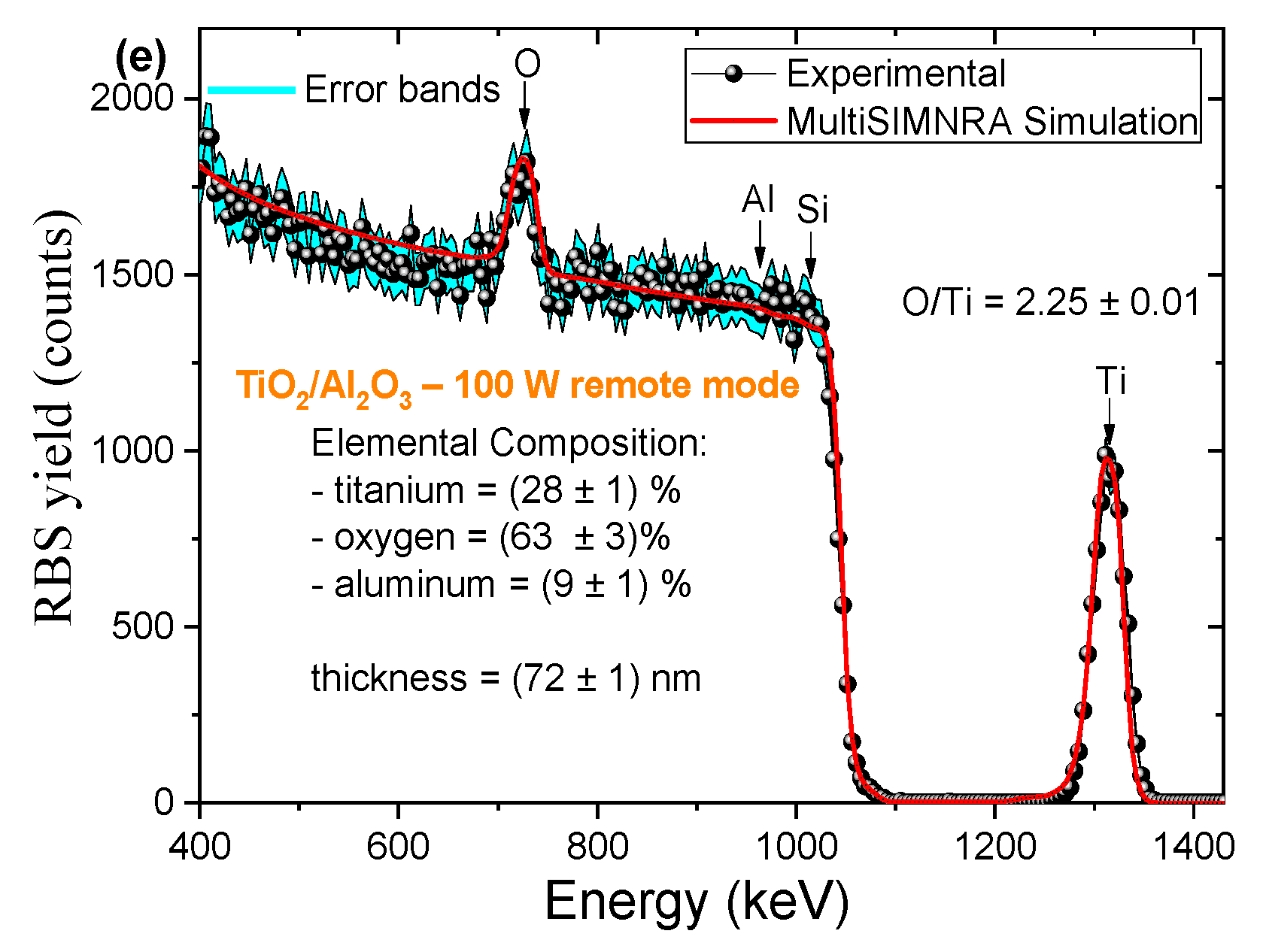
3.1.1. Chemical Composition

Studies of stoichiometry throughout the TiO2 and TiO2/Al2O3 films’ thickness were done, using RBS. Figure 3 shows the experimental and simulated RBS spectra for TiO2 films deposited under different conditions of RF power, plasma mode and Al2O3 partial-monolayer insertion.
The backscattered signal from the TiO2 film on the Si substrate is characterized by well-defined peaks of Ti and O. These peaks depend on the backscattering cross-section, and the areas below the peaks represent the areal density of the atom. Most of the time, the peak position is not matched with the exact energy position of the atom. The Si substrate in the spectra is correlated with the pattern similar to a shoulder. Note that, in the case of TiO2/Al2O3 nanolaminate, the Al peak is not evident; however, it is necessary to consider 9% of its elemental composition during the simulation of the experimental RBS spectrum, as shown in Figure 3e. This behavior occurs because (a) Si and Al have very close atomic numbers that cause an overlapping of their respective peaks, and (b) the amount of Al in the film is low due to the nature of the nanolaminate PEALD process that used a single cycle of TMA-O2 plasma, while repeating 60 cycles of TTIP-O2 plasma during each super-cycle. This results in a low amount of Al in the film (9%), along with the reduced peak intensity in the RBS spectrum. The plasma mode, under the same RF power, does not significantly influence the film thickness. On the other hand, if the RF power is increased, the film thickness is reduced for both plasma modes. This behavior for the TTIP precursor was demonstrated in our previous study [45], where it was observed that the growth per cycle (GPC) decreases when RF power is increased. The leading cause is related to the increase of the density of O2 radicals that fragments the TTIP-ligands, hindering the formation of Ti-O bonds due decreasing of the free path.
The insertion of Al2O3 partial-monolayers in TiO2 using the nanolaminate design proposed by Testoni et al. [49] showed that a considerable increase of number of cycles (2700 cycles) was necessary for obtaining a film thickness near to pure TiO2 condition (1000 cycles). This is due to the poisoning effect promoted by the TMA pulse, affecting the growth kinetics of subsequent TiO2 layers, and thereby altering the overall growth per cycle (GPC) of TiO2/Al2O3 nanolaminate [49].
The elemental chemical composition of the samples is shown, together with the RBS spectra, in Figure 3. The TiOx films show an excess of oxygen, i.e., x values ranging from 2.13 ± 0.01 to 2.33 ± 0.01, as can be seen in Figure 3. These results differ from those described for thermal ALD TiO2 films, in which either stoichometric or oxygen-deficient films are obtained [52]. The increase of oxygen content in PEALD TiO2 films may be related to the higher reactivity of O2 plasma compared to the water precursor used in thermal ALD. In a recent study, Wei et al. [5] showed the influence of temperatures on the PEALD process applied to the growth of TiO2 films in Si for the manufacture of MOS capacitors, where they used O2 plasma at 400 W of RF power. They varied the temperature from 100 to 300 °C, with steps of 50 °C. Using the X-ray photoelectron spectroscopy (XPS) technique, they verified that the TiO2 films had O/Ti stoichiometry ranging from 2.08 to 2.32. These results are in agreement with our O/Ti stoichiometry RBS data. Raztsch et al. [35] found a slight increase in the oxygen content in TiO2 films grown on Si by PEALD with O2 plasma at 300 W. These TiO2 films consist of large crystallites embedded in the amorphous layer, and, through RBS, they determined the O/Ti stoichiometry of 2.00 ± 0.04. Moreover, Bousoulas et al. verified that by increasing the oxygen content in TiO2 films, the size of vacancy-based filaments is reduced, resulting in the more stable operation of resistive switching memory devices [53]. This can be an interesting application for the materials and devices reported in this study, especially for conditions of 100 W RF power and with the insertion of Al2O3. A more detailed explanation of the excess oxygen in the films is given in Section 3.1.2.

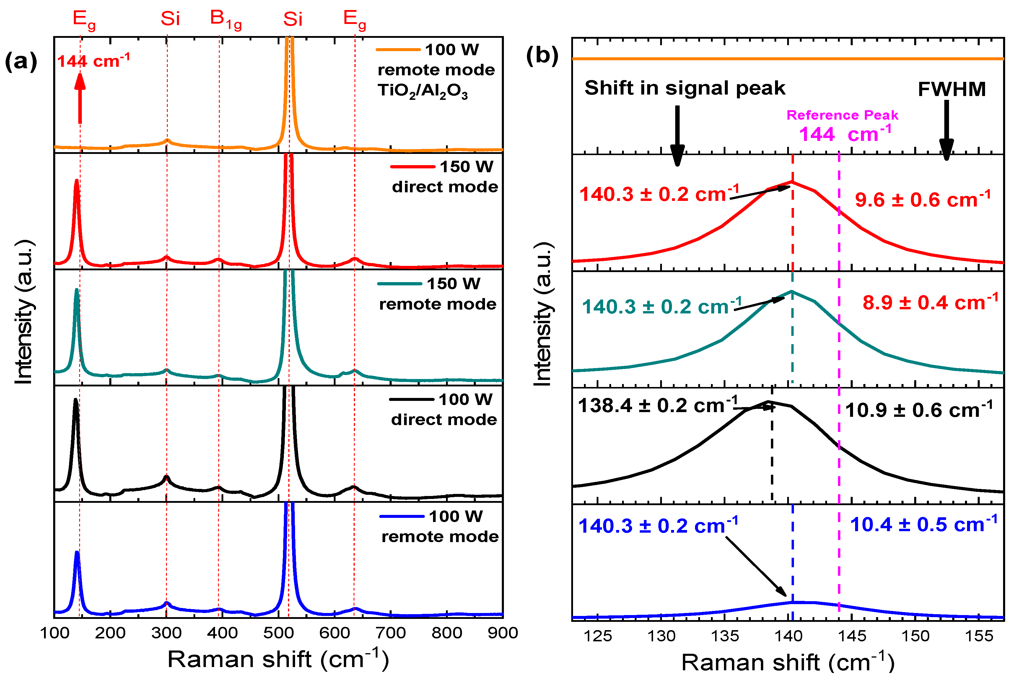
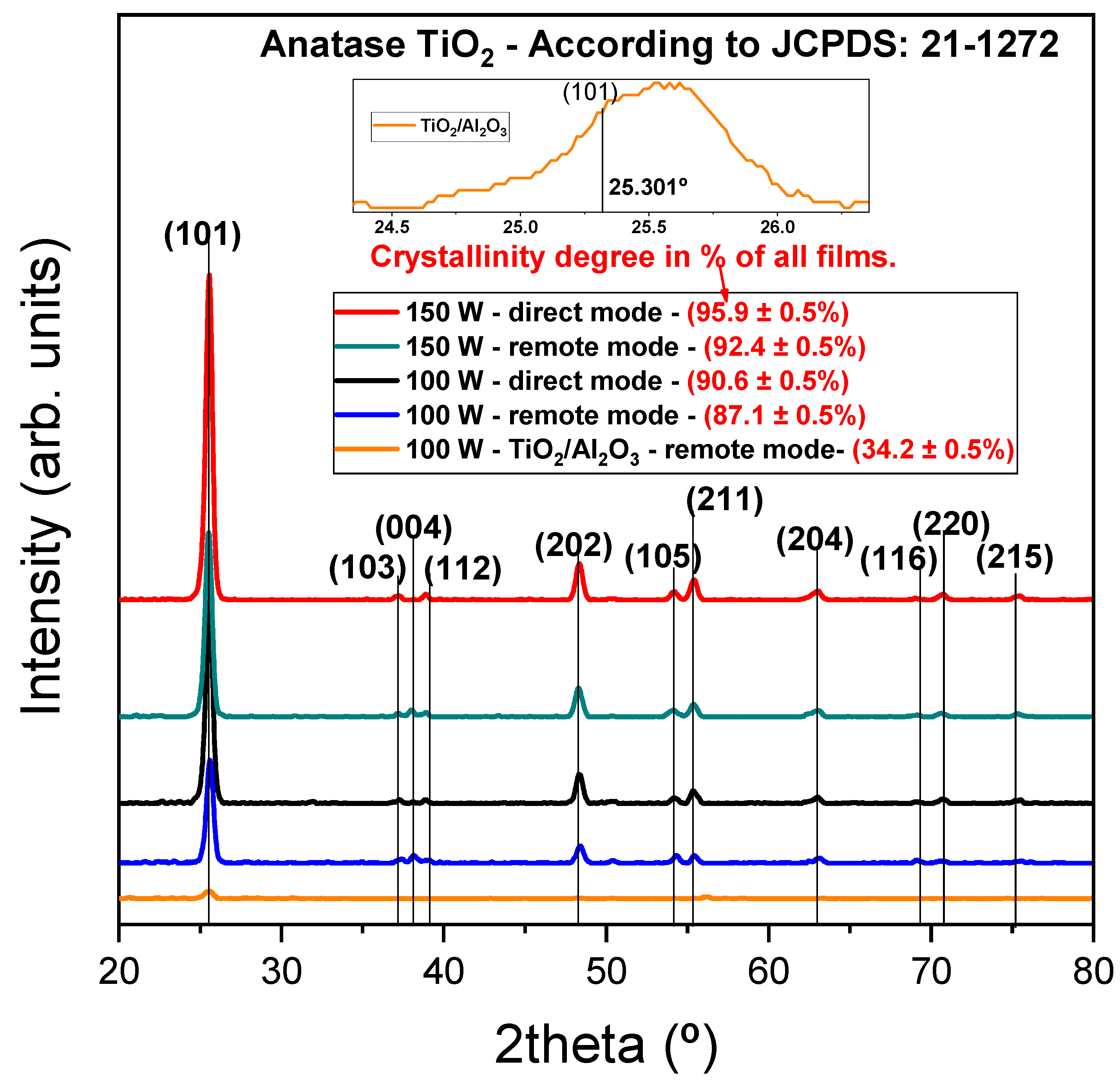
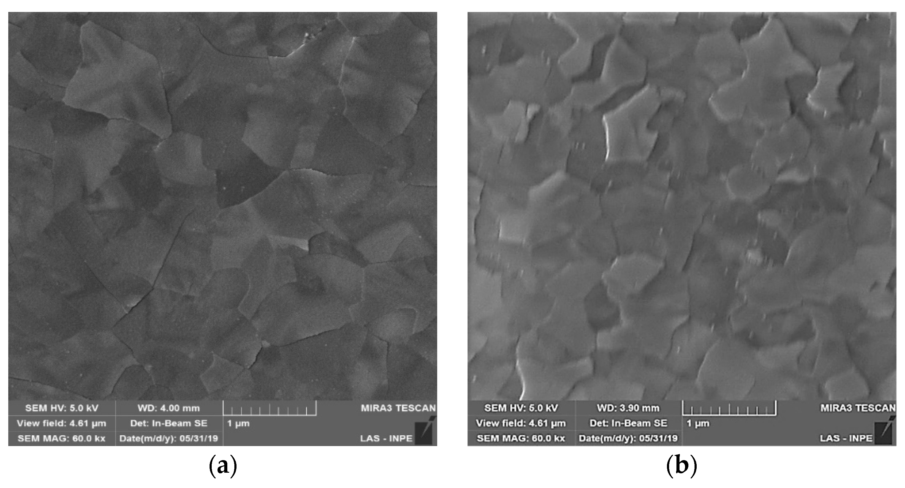
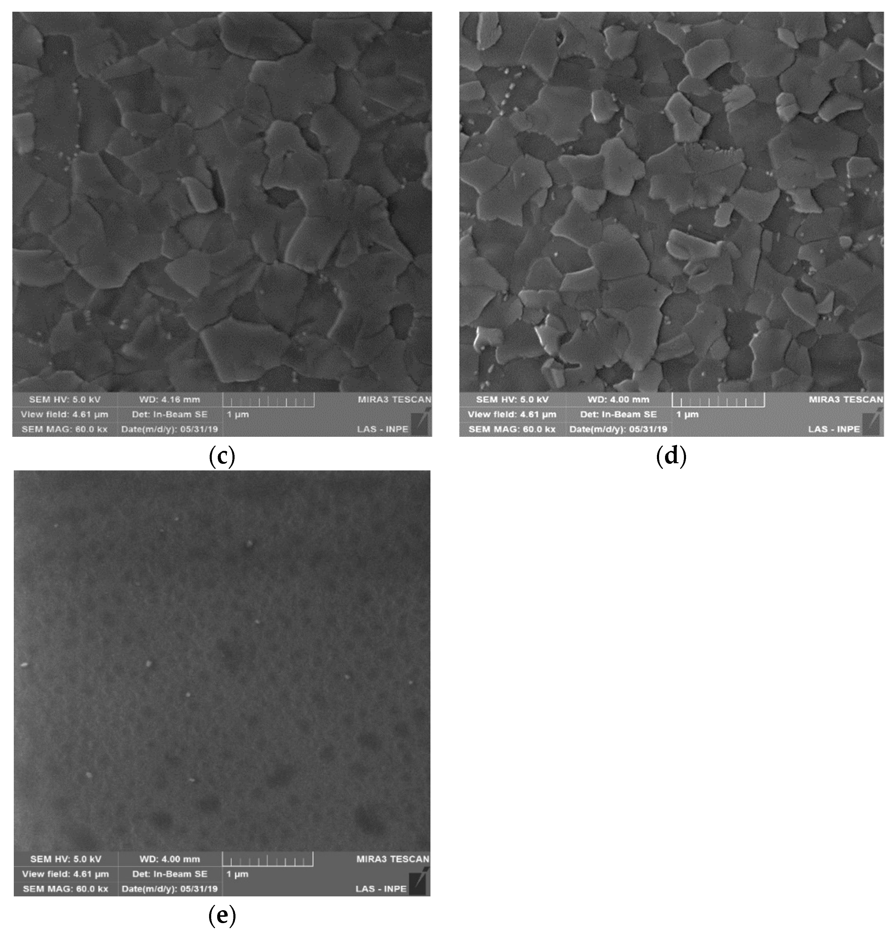
3.1.2. Structure and Morphology

Micro-Raman spectra are shown in Figure 4a. Four Raman-active modes associated with anatase structure can be observed: A1g (519 cm−1), B1g (397 cm−1) and Eg (144 and 636 cm−1) with a strong peak at 144 cm−1 [28,54]. The crystalline condition of pure TiO2 thin films due to the strong peak at 144 cm−1 is clearly evidenced. On the other hand, for the TiO2/Al2O3 nanolaminate, the main peaks of the anatase phase were not observed, and the rutile phase is formed above 500 °C for silicon substrate [28,37,52,53], which suggests that the film is amorphous or partially crystalline. Figure 4b shows the micro-Raman spectra evidencing the shift and the full width at half maximum (FWHM) of the Eg peak at 144 cm−1. According to Parker et al. [55] and Bassi et al. [56], the shift of the Eg peak and bandwidth are related to non-stoichiometry, while the latter also influences the crystal size of anatase TiO2. Ratzsch et al. showed a slight excess in oxygen (O/Ti > 2) in high-density TiO2 with large crystallites embedded in the amorphous layer [35]. They observed the same behavior for the Eg peak at 144 cm−1, i.e., a shift and a broadband. Thus, the shift in the Eg peak and the bandwidth observed in Figure 4b for all PEALD TiO2 films can be attributed to the increase in the oxygen content, corroborating with RBS results. It is noteworthy that all characterizations of the thin films were performed in different positions of the samples. Therefore, the oxygen excess is not localized.
To confirm the Raman results, GIXRD measurements were performed, using the same 0.29° incident angle for all films. This angle was used to reduce the reflections from the Si substrate [45]. Based on the powder diffraction file (JCPDS: 21–1272) [57], all diffraction peaks are identified for the TiO2 films studied here, as shown in Figure 5.
To improve the discussion, the crystallinity degree was calculated, using the following ratio: area of all crystalline peaks/area of all peaks (crystalline and non-crystalline). As can be seen in Figure 5, the films present the following decreasing order of crystallinity degree, (95.9 ± 0.5)% to 150 W—direct mode, (92.4 ± 0.5)% to 150 W—remote mode, (90.6 ± 0.5%) to 100 W—direct mode and (87.1 ± 0.5)% to 100 W—remote mode. These results show a predominance of plasma power over the exposure mode in increasing crystallinity. On the other hand, onto the exposure mode, the direct mode has higher values compared to the remote mode. These results are probably due to the higher incidence of high energy ions for the direct mode. According to Avila et al. [58], the low intensity of the peaks indicated a lower crystallinity, when comparing the relative intensity of the peaks (101), (202) and (211), and the crystallinity degree shows the same behavior, that is, there is a decrease in intensity in the following order: 150 W—direct mode, 150 W—remote mode, 100 W—direct mode and 100 W—remote mode. To better clarify the Raman spectroscopy result on the crystallinity of TiO2/Al2O3 nanolaminate, the GIXRD diffractogram shows (34.2 ± 0.5)% of crystallinity degree, evidencing the partial crystallinity of the TiO2 layers (the inset figure shows the relative intensity of the (101) peak). Therefore, the insertion of Al2O3 partial-monolayer considerably decreases the intensity of (101) peak.
The grain size was calculated by using the Scherrer equation [59]; all the peaks of the anatase phase were considered in the calculations (Figure 5), with the values in the following order: (17.8 ± 0.7) nm to 150 W—direct mode, (19.2 ± 0.9) nm to 150 W—remote mode, (15.9 ± 0.8) nm to 100 W—direct mode and (16.2 ± 0.7) nm. These crystal sizes influence the broadband in Raman peaks [56]; however, when comparing the grain size found in the GIXRD diffractograms with the FWHM of the Eg peak found by the Raman spectrum, it is observed that the larger the grain size is, the smaller the FWHM is. Therefore, the film grown in 150 W—remote mode has the largest grain size with the smallest FWHM. On the other hand, the film grown with 100 W—direct mode has the largest FWHM and the smallest grain size. The results are in agreement with Parker et al. [55] and Bassi et al. [56]. Bearing in mind that there is no Eg peak for the TiO2/Al2O3 film, and the error associated with the grain size is higher than the grain value, we could not find these parameters for this film.
Figure 6 shows FESEM images of the surface of the TiO2 films grown at different PEALD process conditions. These images show that the grain size slight decreases with RF power for both plasma modes. The effect of the electrode grid was evidenced by the reduction of the action of the plasma ions during the capacitively coupled PEALD process [45]. As can be seen for both power values investigated, the change from remote to direct mode caused a slight reduction in grain size, probably due to the higher action of the species from plasma impinging on the substrate. An interesting result is presented in Figure 6e, where the insertion of Al2O3 partial-monolayers into TiO2 film disrupts the growth of crystalline grains, creating only a few nanocrystalline grains in amorphous matrix [49].

3.2. Electrical Characterization of TiO2/p-Si MOS Capacitors

3.2.1. Current Density-Voltage Measurements

Electrical characterization was performed on the five PEALD TiO2/p-type Si MOS structures fabricated at different values of RF power, substrate exposure mode and Al2O3 partial-monolayer insertion. Two sets of MOS current density were analyzed and presented in Figure 7: (i) one for TiO2 samples with RF powers at 100 W and 150 W for remote and direct plasma modes (Figure 7a), and (ii) another for TiO2/Al2O3 nanolaminate (Figure 7b). Figure 7d shows the dark J-V curve in semi-logarithmic scale under positive and negative biases at room temperature. As can be seen, the leakage current density at −2 V is in the order of 10−5~10−4 A/cm2, which is in the same order of magnitude reported by Wei et al. [5] and Baek et al. [1] that used PEALD and tetrakis dimethylamino titanium (TDMAT) as precursor to growth TiO2 (20 nm) on Si.
To study the diode ideality factor (n), we used the dark J-V-adapted Ortiz-Conde model [60], which considers the equivalent circuit model, consisting of a single exponential type ideal junction, a series parasitic resistance (Rs) and a parallel parasitic conductance (Gp), as shown in Figure 7c. The J(V) function of the equivalent circuit model is given by the following equation:
J = J 0 ( exp ( V J R s n V t h ) 1 ) + ( V J R s ) G p
where J is the current density, V is the terminal voltage, J0 is the reverse saturation current density and V t h = k T q is the thermal voltage.
This implicit transcendental function cannot be explicitly resolved by using a standard elementary function. The solution depends on a particular function known as the Lambert W function [61]. By definition, this function is defined as the solution of the Lambert W (x) exp (Lambert W(x)) = x, where the solutions for each variable, J and V, are an explicit function of the other. Using the auxiliary Equation (1), we obtain the parameters a, b, c and d as a function of the equivalent circuit model:
a = 1 + R s G p J 0
b = J 0 V . G p J 0 ,
c = R s n V t h ,
d = V n V t h ,
The general solution is as follows:
J = n V t h R s L a m b e r t W ( J 0 R s n V t h ( 1 + R s G p ) exp ( V + J 0 R s n V t h ( 1 + R s G p ) ) ) + V G p J 0 ( 1 + R s G p )
This explicit analytic expression can be used to extract model parameters (Table 1) directly from the fit of experimental data, as shown in Figure 7c.
Table 1 presents the diode ideality factor for all dark J-V curves fitted by Equation (6). As can be seen in Table 1, the ideality factor values occur between 1 and 2. Second, in the Shockley diffusion theory, which is based on the minority carrier diffusion predicted, n should be equal to 1 (next to an ideal junction) [62]. Sah et al. analyzed the generation and recombination in the space charge layer and predicted that n ≤ 2 [63]. Faulkner and Buckingham [64] proposed a theory based in traps situated in depletion layer where the values of diode ideality factor occur between 1 and 2, which was experimentally verified by Nussbaum [65]. According to the aforementioned theories, the Ortiz-Conde model adjusted the experimental curves with good precision.
For 100 W RF power, ideality factor values decreased when the exposure mode changed from direct to remote. As the physical, chemical and morphological properties of the TiO2 films synthesized in direct or remote mode are close, it is believed that the variation of n occurred because of changes in the sample’s electrical properties, as reported in Table 1. Indeed, the mode change, as well as the RF power change, modified the Rs and Gp values of the films, where for 100 W RF power/direct mode, the series parasitic resistance achieved 180 Ω. On the other hand, for TiO2/Al2O3 nanolaminate, the ideality factor was of 1.59, which suggests that the insertion of Al2O3 partial-monolayers can be used to adjust the n parameter. According to Jain and Kappor [66] and Shockley [62], n closer to 1 is more efficient for DRAM capacitors and solar cell devices. In addition, Table 1 shows that this sample has a higher series parasitic resistance of 1100 Ω.

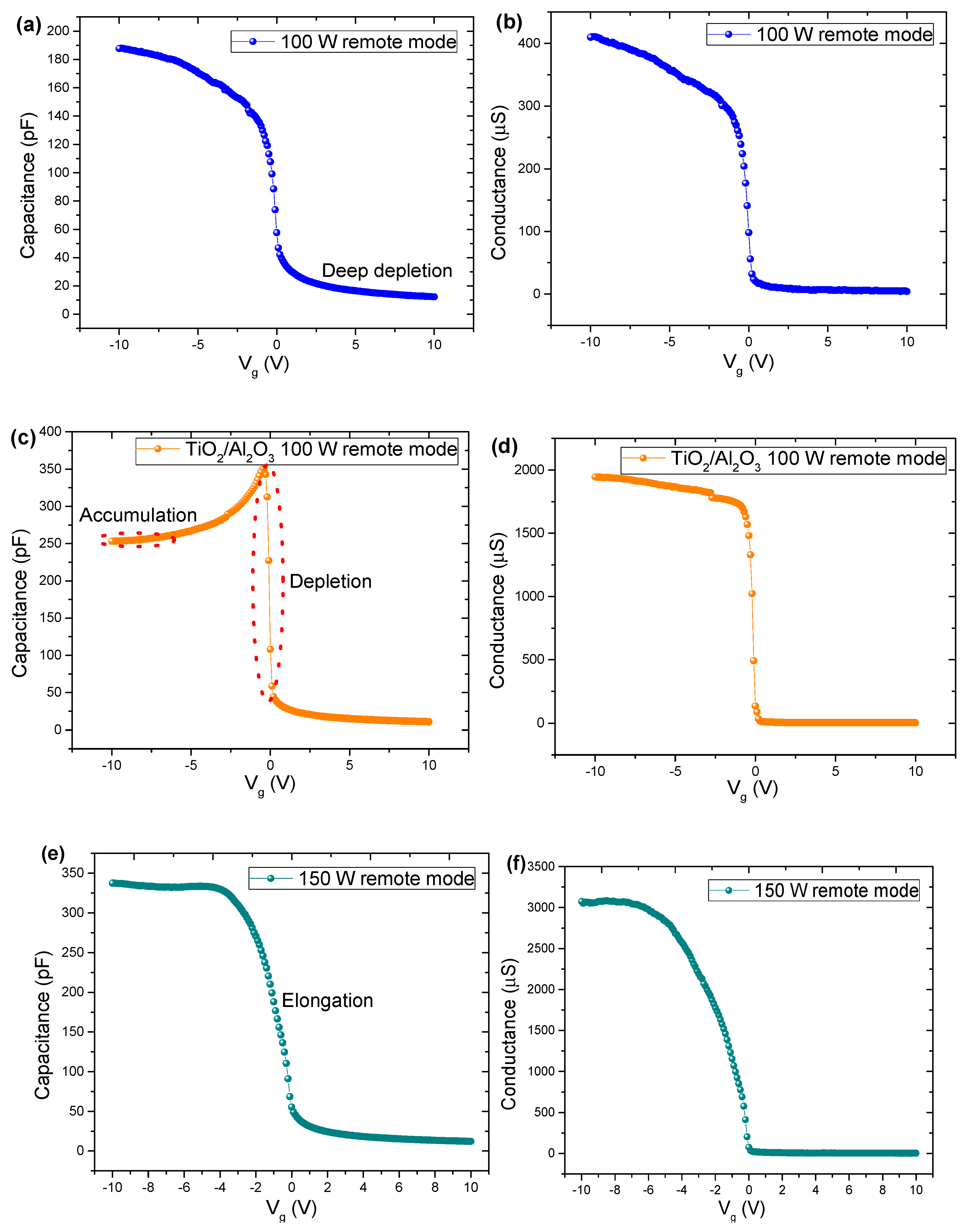
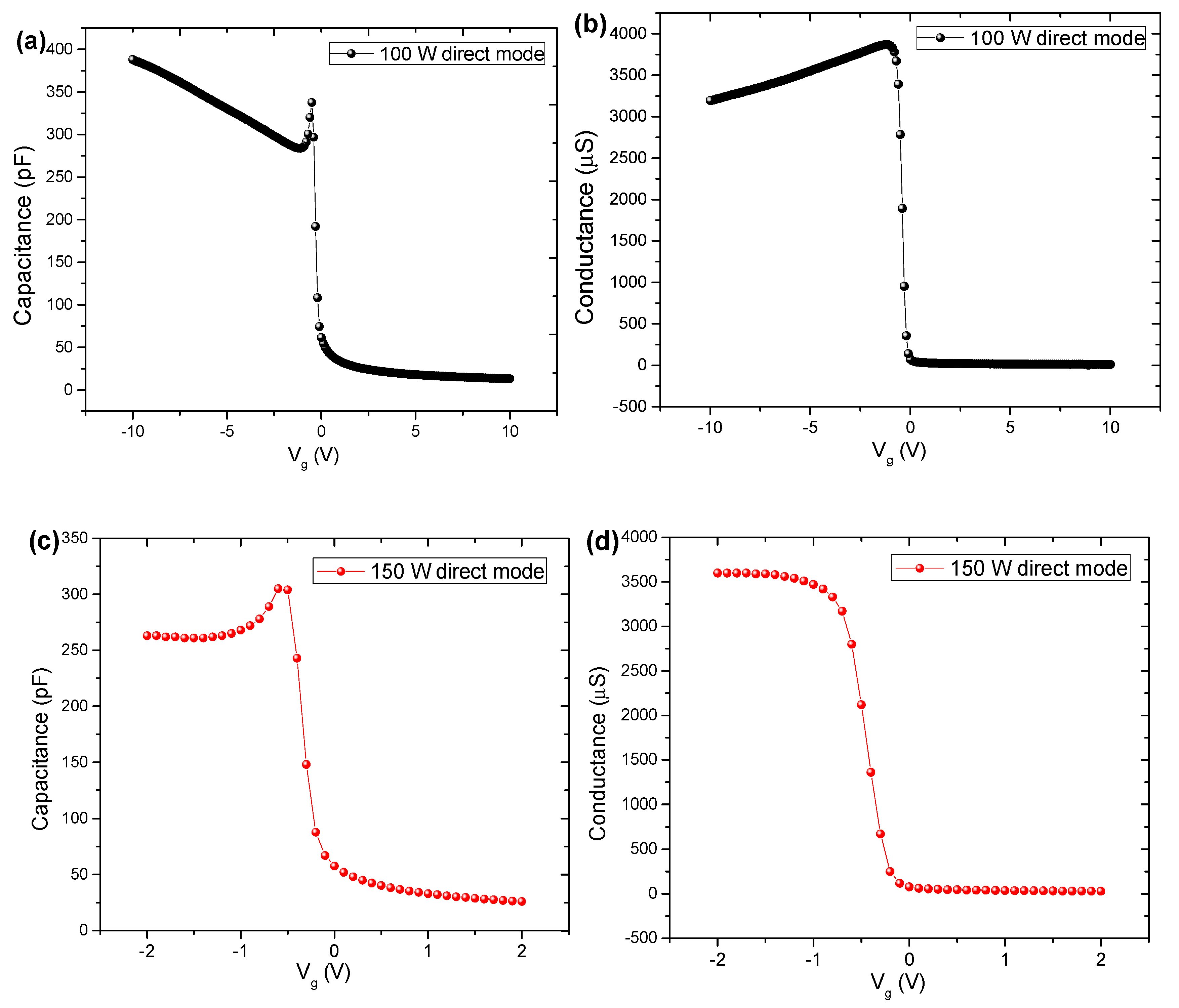
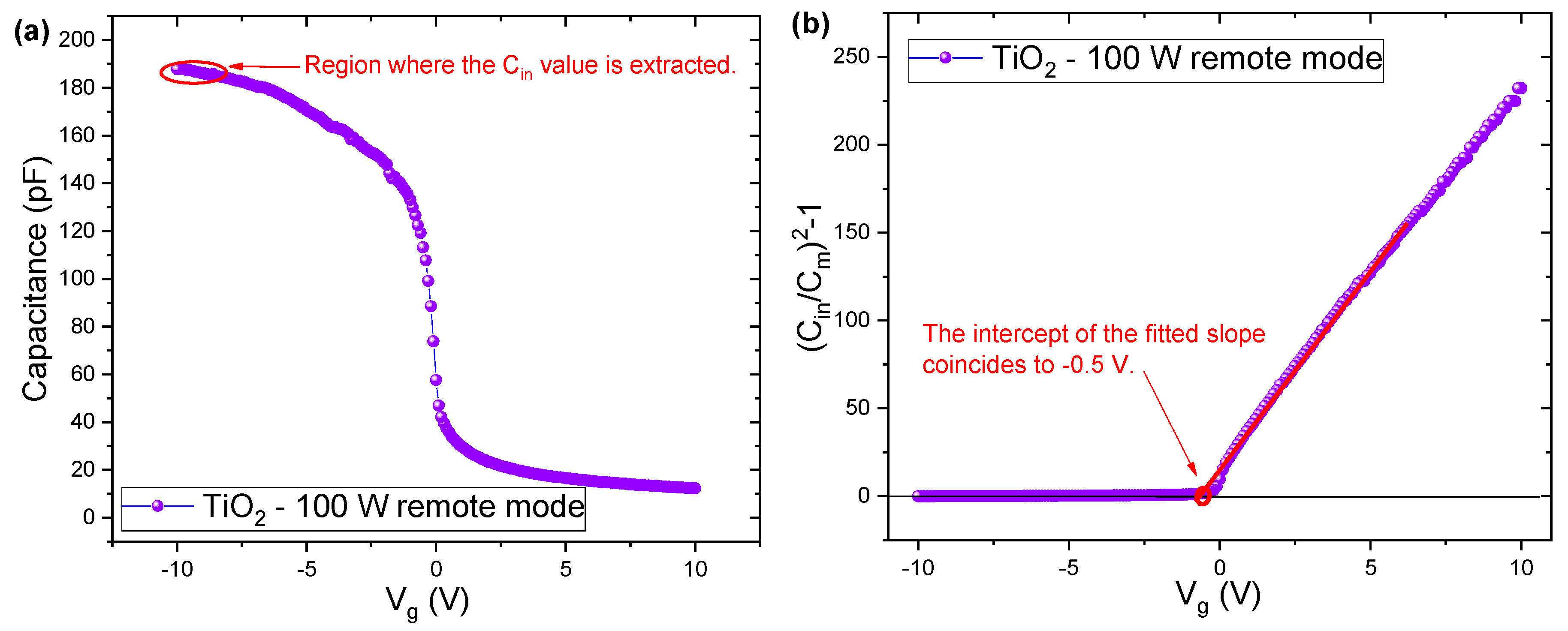
3.2.2. Capacitance-Voltage and Conductance-Voltage Measurements

C-V and G-V measurements were also performed to evaluate the electrical characteristics of the fabricated MOS capacitors. All the samples have presented a leakage current process through the TiO2 layer.
Figure 8 shows the C-V and G-V curves for samples deposited in remote mode. The C-V curves showed a deep depletion region for all investigated cases, indicating the absence of an inversion layer due to the high leakage current through the TiO2 films. By comparing the behavior of the C-V curve with the G-V curve for TiO2 grown at 100 W in remote mode (Figure 8a,b), it can be seen that capacitance does not stabilize on a plateau, because of increased conductance in the same region. The leakage increasing in conductance with negative voltage (Figure 8b) is related to the effect of the rise of the capacitance in this region, being an order of magnitude smaller compared to the curves in Figure 8d,f, suggesting a reduction of the series resistance in the area of accumulation [67]. The sample with Al2O3 partial-monolayer grown at 100 W (Figure 8c,d) presented a high leakage current that decreased the accumulation capacitance. This higher leakage current in the accumulation region occurs due to a negative gate bias applied to the silicon p-type substrate. The majority carriers are attracted to the interface Si/TiO2/Al2O3 with simultaneously accumulated minority carriers at the gate side flow through the TiO2/Al2O3 layer, thus reducing the majority carriers’ density at the interface of Si/TiO2/Al2O3. With the increase of gate bias, the accumulated majority carriers disappear, and a negative depletion region is formed in the silicon, which promotes a decrease of the leakage current and an increase of the capacitance, as shown by the peak in C-V curve (Figure 8c). In Figure 8e, an elongation in the C-V curve can be observed, which can be attributed to the existence of surface states in the TiO2 thin films [68]. This behavior may be associated with increased ion damage due to the RF power at 150 W. For TiO2 film growth at 150 W in remote mode, the C-V curve does not show any evidence of a decrease of the accumulation capacitance that allows to infer a drastic reduction of the leakage current. This reduction can be attributed to a structural rearrangement of the growth of the films at 150 W that reduced the series parasitic resistance (as shown in Table 1).
C-V and G-V curve characteristics for the samples deposited under direct exposure mode are shown in Figure 9. For capacitors with TiO2 films grown at 150 W in direct mode, the C-V and G-V curves were only possible to be obtained in the range of −2 V to +2 V. The C-V curves (Figure 9a,c) showed a deep depletion region for both cases, as the behaviors for PEALD TiO2/Si MOS capacitors with TiO2 films grown in direct mode indicated a current leakage through the TiO2 films. The sample with TiO2 grown at 100 W in direct mode (Figure 9a) presented a low leakage current that raised the accumulation capacitance. This low leakage current in the accumulation region occurs due to an abrupt decreasing in conductance in the same negative bias region of the gate (Figure 9b). When the gate bias increase, the accumulation of the majority carriers disappears, and a negative depletion region is formed on the silicon, promoting a decrease in leakage current and an expansion of the capacitance, as shown by the peak in the C-V curve (Figure 9a).
Compared to the 100 W TiO2 thin film grown in remote mode, an increase in conductance by one order of magnitude occurs, probably due to the high ion bombardment caused by the direct exposure mode (Figure 9b). The insertion of Al2O3 partial-monolayers in TiO2 film modulated the conductance (Figure 8d), with the maximum value of conductance at the ~2000 µS being between the values of TiO2-100 W in remote mode (~400 µS) and TiO2-100 W in direct mode (~4000 µS). It is noteworthy that for the sample grown at 150 W, in the direct mode, the same behavior in curves C-V and G-V was observed in relation to nanolaminate.
To better understand the electrical properties, we estimated another two parameters: (i) fixed insulator (TiO2 and TiO2/Al2O3) charges, Qf; and (ii) the interface defects density, Dit, in the Si/insulator interface. We used Equation (7) to calculate Qf, and to obtain the Vfb, we used the graphical method, which is shown in Figure 10 [66].
Q f = C i n ( Φ m s V f b ) A . q
where Cin is the capacitance of the insulator, A (4.3 × 10⁻³ cm2) is the front metal contact area, q is the elementary charge, Vfb is the flat-band voltage, Φms is the work function difference between the work function of metal (Al) and the work function of the semiconductor (Si) that was calculated from Equation (8) [69].
Φ m s = 0.6 k T q ln ( N A n i ) ,
where NA is the doping concentration in the silicon (NA = 1.0 × 1015 cm−3), and ni is the intrinsic concentration at room temperature (ni = 1.45 × 1010 cm−3) [68,70]. To use Equation (7), it was assumed, but not yet proved, that other charges have a reduced influence on Qf measurements, and the interface traps are negligible [71,72,73,74]. The graphical method was used to find the Qf values, taking into account the average of Vfb and Cin.
As can be seen in Figure 10a, the insulator capacitance value was extracted from the strong accumulation region in the C-V curve at negative bias due to the conductivity nature p-type of the silicon. To construct Figure 10b and extract the flat-band voltage, the following equation was used:
( C i n C m ) 2 1 = 0 ,
where Cm is the experimentally measured capacitance. To calculate Cin and, consequently, Qf, in the strong leakage processes from the capacitance lowering at the accumulation region of the C-V curves (Figure 7c and Figure 8a,c), the Rajab Model was used [67]. To observe the leakage process, the Rajab model proposed a simplified electrical model, as shown in Figure 11a, where YC is an admittance which represents the leakage process, and RS is the series resistance associated with the silicon substrate. Gm,max and Cm,max in Figure 11b are the accumulation conductance and capacitance, respectively, shown from a C-V meter.
Using the impedance equality of the electrical circuits shown in Figure 10a,b, we derived the equations for the leakage admittance YC and Cin, which are shown below [67]:
Y C = ω C i n ( ω C i n + ω C m ,   m a x ( 1 + G m ,   m a x 2 ( ω C m ,   m a x ) 2 ) ) ,
and
C i n =   C m ,   m a x ( ( ω C m ,   m a x ) 2 + G m ,   m a x 2 ) ( ω C m ,   m a x ) 2 + ( G m ,   m a x R S ( ( ω C m ,   m a x ) 2 + G m ,   m a x 2 ) ) .
Table 2 shows the Vfb and Qf values of all samples with the front contact area of 4.3 × 10⁻³ cm2. As shown in the literature, TiO2 grown on Si generates negative Qf being more appropriate for rear passivation in solar cells, basically due to field-effect passivation [45]. Recently, Liao et al. [73] showed that TiOx thin-film (63 nm) growth by ALD is also capable of providing passivation of c-Si substrates at the same level of thermal silicon oxide (SiO2), silicon nitride (SiNx) and aluminum oxide (Al2O3). This negative polarity corroborates with the best passivation performance in solar cells because negative Qf repels minority carriers (electrons), resulting in an increased level of field-effect passivation [74].
As can also be seen in Table 2, the exposure mode influences the values of the fixed charges but did not change the polarity. The increase in leakage in conductance with the negative voltage (Figure 7b) is related to the effect of the rise of the capacitance in this region of conductance that causes a reduced value in Qf around 1 × 1011 cm−2 for the TiO2-100 W in remote mode. The higher values were of the samples that grown in direct mode around 1 × 1012 cm−2 for both RF powers values. For the samples that grew at 100 W, a behavior similar to that of J-V curves was observed where the Al2O3 partial-monolayer modulated the values of the ideality factor. In this case, the Al2O3 partial-monolayer obtained a magnitude above the Qf value obtained for TiO2-100 W in remote mode and one order of magnitude below the value obtained for the TiO2-100 W in direct mode (as shown in Table 2), acting as a modulator between the two cases. As can be seen in Table 2, this analysis indicates that the fixed insulator charge values are not intrinsic to each insulator, and its concentration can be modified by exposure mode and plasma power.
Another critical parameter for the interface is the density of interface defects (Dit). For this, it was used the Hill–Coleman model [74], a single-frequency approximation for interface defects density determination, as shown below:
D i t = 2 A . q G m ,   m a x ω ( G m , m a x ω . C i n ) 2 + ( 1 C m , m a x C i n ) 2 ,
where Gm,max is the maximum experimentally conductance, Cm,max is the maximum experimentally capacitance and ω = 2πf (f = 1 MHz).
The advantage of this model is that only three measured values (Gm,max, Cm,max and Cin) and a single frequency are needed. Therefore, the approximation is realized from the need of C-V and G-V plots. Table 3 summarizes the Dit values extracted with the help of Equation (12).
Most of the samples show Dit values within the same order of magnitude, being the exception of the TiO2-100 W in remote mode. This exception probably occurs due to the approximation technique for Dit is within 25–30% of the Nicollian–Brews peak Dit’s value between the flat band and mid-gap [71]. Since Dit is known to change by order of magnitude or more in the region between the flat band and mid-gap, this approximation is reasonable [74]. As suggested by Hill–Coleman, the frequency is into the MHz region. The results listed in Table 2 and Table 3 show that the samples exhibit a density of interface defects (~1011–1013 cm−2) and a high density of negative fixed charges (~1011 eV−1.cm−2), which make them potential candidates for application in solar cells and DRAM technology. For example, TiO2-100 W and TiO2-150 W growth by the direct mode presents higher Qf and lower Dit. These combined characteristics show the quality of these films to act as a passivation layer in solar cells. Cunha et al. [42] and Kotipali et al. [72] showed values in the same order of magnitude for Qf (~1011–1012 cm−2) and Dit (~1010–1012 eV−1 cm−2) for other thin films, namely Al2O3, Si3Nx and SiOx. In both works, the films were grown on Si and CIGS.
To improve the discussion, we compared our results with works that used chemical and thermal treatments to enhance the electrical properties of the following structures Al2O3/Si and TiO2/Al2O3/Si. Yoshitsugu et al. [76] deposited Al2O3 (25.2 nm) on Si by PEALD at a fixed temperature of the 100 °C and RF power at 400 W. They used high-pressure deuterium oxide annealing (HPDOA) treatment and reduced the leakage current density to an order of 10−7 A/cm2. This result is two orders of magnitude lower than our results. Zougar et al. [77] deposited Al2O3 (~1 nm) on Si by the ultrasonic spray method. They used post-deposition annealing and post-metallization annealing as surface treatment. They showed values of for Qf (~1010–1011 cm−2) and Dit (~1011–1012 eV−1 cm−2). Both results show a lower quality of these films in comparison with our films. Baek et al. [1] grew Al2O3 (50 nm), TiO2 (50 nm) and Al2O3/TiO2 (50 nm) on Si by PEALD at 100 °C and with RF power fixed at 200 W. They used several chemical treatments to modify the surface. The leakage current density values of Al2O3 and Al2O3/TiO2 are, respectively, 10−8 and 10−9 A/cm2. These values are lower than our results, but they showed a leakage current density of the TiO2 of the order of magnitude of 10−3 A/cm2, which is two orders of magnitude higher than our values. Even without thermal or chemical treatment, our films have a high electrical quality, as shown in this brief comparison.

4. Conclusions

TiO2 thin films were deposited on p-type Si substrates under different conditions by PEALD technique. Structural, chemical and morphological properties of the as-grown films were studied as a function of the following deposition parameters: RF power, substrate exposure mode and Al2O3 partial-monolayer insertion. Chemical composition determined by RBS analysis showed that the TiOx films have an excess of oxygen content, with x values ranging from 2.13 ± 0.01 to 2.33 ± 0.01, which can be related to the higher reactivity of O2 plasma. It was also observed that, with the insertion of Al2O3 partial-monolayers in TiO2 to form the nanolaminate structure, an increase in the number of cycles to 2700 is necessary to obtain a film thickness close to pure TiO2. GIXRD diffractograms showed a crystalline structure for all pure TiO2 thin films with a crystalline degree of 87.1% to 95.9%. The Al2O3 partial-monolayer reduced TiO2 crystallinity degree to 34.2%. Raman spectra allow us to observe that the shift in the signal peak at 144 cm−1 and its bandwidth is related to the increase of oxygen content in PEALD TiO2 films. FESEM study evidenced the effect of the electrode grid on the reduction of the action of the plasma ions during the capacitively coupled PEALD process. It can be seen, for both power values investigated, that the change from remote to direct mode caused a slight reduction in grain size, probably due to the more significant action of species impinging from plasma to substrate. The insertion of Al2O3 partial-monolayers into TiO2 film disrupts the growth of crystalline grains, creating only a few nanocrystalline grains in the amorphous matrix. PEALD TiO2/p-type Si MOS capacitors were fabricated by depositing of Al electrical contacts. J-V, C-V and G-V measurements of these capacitors were performed. The Ortiz-Conde model was used to fit the experimental dark J-V curves and values between 1.59 to 1.99 were obtained for the ideality factor. For TiO2 thin-film growth at RF power of 150 W, the values did not change with the exposure mode, and this behavior suggests that the power effect is predominant in the process. For the sample TiO2-100 W, different values of the ideality factor were found: 1.93 (direct mode) and 1.79 (remote mode). For the TiO2/Al2O3 nanolaminate, the ideality factor was 1.59, suggesting that the insertion of Al2O3 partial-monolayers can tune the ideality factor. C-V and G-V curves showed a deep depletion region for all cases, which indicates the absence of a layer of inversion because of the high leakage of electrons through the TiO2 films. It was noted that Al2O3 partial-monolayer, grown at 100 W, modulated the conductance with the maximum value of ~2000 µS, whereas a value of ~400 µS and ~4000 µS were found for TiO2-100 W in remote mode and TiO2-100 W in direct mode, respectively. The fixed insulator charges (Qf) and the interface defects density (Dit) were also estimated. In summary, the fabricated PEALD TiO2/p-type Si MOS capacitors exhibit electrical characteristics suitable for microelectronics and photovoltaics applications.

Author Contributions

All authors have read and agree to the published version of the manuscript. Conceptualization, W.C. and S.d.S.F.; methodology, W.C. and R.P.; formal analysis, W.C., V.D., G.T., R.P., M.W. and R.R.; investigation, W.C., V.D., M.F., G.T., R.P. and M.W.; resources: H.M., S.d.S.F. and R.P.; writing—original draft, W.C.; writing—review and editing, W.C., R.P., M.F., H.M. and S.d.S.F.; supervision, S.d.S.F. and R.P.; funding acquisition, H.M., S.d.S.F., R.P. and M.F.

Funding

The financial support of the Brazilian agency program FAPESP/MCT/CNPq-PRONEX (grant no. 2011/50773-0), FAPESP (grant no. 2015/05956-0, no. 2015/10876-6, no. 2016/17826-7, and no. 2018/01265-1), CNPq (grant no. 305496/2012-3, 446545/2014-7 and 437921/2018-2), CAPES (grant no. 23038.005802/2014-98) and the Brazilian Space Agency (AEB/Uniespaço) is also gratefully acknowledged.

Acknowledgments

The authors are grateful to T.F. da Silva from the Physics Department—USP for the RBS measurements and I.Y. Abe from LME-USP for the Raman spectroscopy measurements.

Conflicts of Interest

The authors declare no conflicts of interest.

References

  1. Baek, Y.; Lim, S.; Kim, L.H.; Park, S.; Lee, S.W.; Oh, T.H.; Kim, S.H.; Park, C.E. Al2O3/TiO2 nanolaminate gate dielectric films with enhanced electrical performances for organic field-effect transistors. Org. Electron. 2016, 28, 139–146. [Google Scholar] [CrossRef]
  2. Wei, D.; Edgar, J.H.; Briggs, D.P.; Retterer, S.T.; Srijanto, B.; Hensley, D.K.; Meyer, H.M., III. Atomic layer deposition TiO2-Al2O3 stack: An improved gate dielectric on Ga-polar GaN metal oxide semiconductor capacitors. J. Vac. Sci. Technol. B 2014, 32, 060602. [Google Scholar] [CrossRef]
  3. Jeong, H.Y.; Kim, Y.I.; Lee, J.Y.; Choi, S.-Y. A low-temperature-grown TiO2-based device for the flexible stacked RRAM application. Nanotechnology 2010, 21, 115203. [Google Scholar] [CrossRef] [PubMed]
  4. Zhang, W.; Kong, J.-Z.; Cao, Z.-Y.; Li, A.-D.; Wang, L.-G.; Zhu, L.; Li, X.; Cao, Y.-Q.; Wu, D. Bipolar resistive switching characteristics of HfO2/TiO2/HfO2 trilayer-structure RRAM devices on Pt and TiN-coated substrates fabricated by atomic layer deposition. Nanoscale Res. Lett. 2017, 12, 393. [Google Scholar] [CrossRef] [PubMed]
  5. Wei, D.; Hossain, T.; Garces, N.Y.; Nepal, N.; Meyer, H.M., III; Kirkham, M.J.; Eddy, C.R., Jr.; Edgar, J.H. Influence of atomic layer deposition temperatures on TiO2/n-Si MOS capacitor. ECS J. Solid State Sci. Technol. 2013, 2, N110–N114. [Google Scholar] [CrossRef] [Green Version]
  6. Maeng, W.J.; Kim, W.-H.; Lim, S.J.; Lee, C.-S.; Lee, T.; Kim, H. Flatband voltage control in p-metal gate metal-oxide-semiconductor field effect transistor by insertion of TiO2 layer. Appl. Phys. Lett. 2010, 96, 082905. [Google Scholar] [CrossRef] [Green Version]
  7. Zardetto, V.; Williams, B.L.; Perrota, A.; Di Giacomo, F.; Verheijen, M.A.; Andriessen, R.; Kessels, W.M.M.; Creatore, M. Atomic layer deposition for perovskite solar cells: Research status, opportunities, and challenges. Sustain. Energy Fuels 2017, 1, 30–55. [Google Scholar] [CrossRef]
  8. Wang, W.-C.; Tsai, M.-C.; Yang, J.; Hsu, C.; Chen, M.-J. Efficiency enhancement of nanotextured black silicon solar cells using Al2O3/TiO2 dual-layer passivation stack prepared by atomic layer deposition. ACS Appl. Mater. Interfaces 2015, 7, 10228–10237. [Google Scholar] [CrossRef]
  9. Pessoa, R.S.; Fraga, M.A.; Santos, L.V.; Massi, M.; Maciel, H.S. Nanostructured thin films based on TiO2 and/or SiC for use in photoelectrochemical cells: A review of the material characteristics, synthesis and recent applications. Mater. Sci. Semicond. Process. 2015, 29, 56–68. [Google Scholar] [CrossRef]
  10. Nakata, K.; Fujishima, A. TiO2 photocatalysis: Desing and applications. J. Photochem. Photobiol. C 2012, 13, 169–189. [Google Scholar] [CrossRef]
  11. Daghrir, R.; Drogui, P.; Robert, D. Modified TiO2 for environmental photocatalytic applications: A review. Ind. Eng. Chem. Res. 2013, 52, 3581–3599. [Google Scholar] [CrossRef]
  12. Pessoa, R.S.; Fraga, M.A.; Chiappim, W.; Maciel, H.S. Exploring the Properties and Fuel Cell Applications of Ultrathin Atomic Layer Deposited Metal Oxide Films. In Emerging Materials for Energy Conversion and Storage, 1st ed.; Cheong, K.Y., Impellizzeri, G., Fraga, M.A., Eds.; Elsevier: Cambridge, MA, USA, 2018; pp. 83–114. [Google Scholar]
  13. Sharma, R.K.; Bhatnagar, M.C.; Sharma, G.L. Influence of doping on sensitivity and response time of TiO2 oxygen gas sensor. Rev. Sci. Instrum. 1999, 71, 1500–1509. [Google Scholar] [CrossRef]
  14. Bao, S.-J.; Li, C.M.; Zang, J.-F.; Cui, X.-Q.; Qiao, Y.; Guo, J. New nanostructured TiO2 for Direct electrochemistry and glucose sensor applications. Adv. Funct. Mater. 2008, 18, 591–599. [Google Scholar] [CrossRef]
  15. Fraga, M.A.; Furlan, H.; Pessoa, R.S.; Rasia, L.A.; Mateus, C.F.R. Studies on SiC, DLC and TiO2 thin films as piezoresistive sensor materials for high-temperature applications. Microsyst. Technol. 2012, 8, 1027–1033. [Google Scholar] [CrossRef]
  16. Rathee, D.; Kumar, M.; Arya, S.K. CMOS development and optimization, scaling issue and replacement with high-k material for future microelectronics. Int. J. Comput. Appl. 2010, 8, 10–17. [Google Scholar] [CrossRef]
  17. Pfeiffer, K.; Schulz, U.; Tünnermann, A.; Szeghalmi, A. Antireflection coating for strongly curved glass lenses by atomic layer deposition. Coatings 2017, 7, 118. [Google Scholar] [CrossRef] [Green Version]
  18. Pessoa, R.S.; Fraga, M.A. Biomedical applications of ultrathin atomic layer deposited metal oxide films on polymeric materials. In Frontiers of Nanoscience, 1st ed.; Benelmekki, M., Erbe, A., Eds.; Elsevier: Cambridge, MA, USA, 2019; Volume 14, pp. 291–307. [Google Scholar]
  19. Pessoa, R.S.; dos Santos, V.P.; Cardoso, S.B.; Doria, A.C.O.C.; Figueira, F.R.; Rodrigues, B.V.M.; Testoni, G.E.; Fraga, M.A.; Marciano, F.R.; Lobo, A.O.; et al. TiO2 coatings via atomic layer deposition on polyurethane and polydimethylsiloxane substrate: Properties and effects on C. Albicans growth and inactivation process. Appl. Surf. Sci. 2017, 422, 73–84. [Google Scholar] [CrossRef]
  20. Dias, V.; Maciel, H.S.; Fraga, M.A.; Lobo, A.O.; Pessoa, R.S.; Marciano, F.R. Atomic layer deposited TiO2 and Al2O3 thin films as a coating for Aluminum food packing application. Materials 2019, 12, 682. [Google Scholar] [CrossRef] [Green Version]
  21. Uchiyama, H.; Bando, T.; Kozuka, H. Effect of the amount of H2O and HNO3 in Ti(OC3H7i)4 solutions on the crystallization of sol-gel-derived TiO2 films. Thin Solid Film. 2019, 669, 157–161. [Google Scholar] [CrossRef]
  22. Abbas, F.; Bensaha, R.; Taroré, H. The influence of Zn+2 doping and annealing temperature on grown-up of nanostructures TiO2 thin films prepared by the sol-gel dip-coating method and their photocatalytic application. Optik 2019, 180, 361–369. [Google Scholar] [CrossRef]
  23. Toku, H.; Pessoa, R.S.; Maciel, H.S.; Massi, M.; Mengui, U.A. The effect of oxygen concentration on the low temperature deposition of TiO2 thin films. Surf. Coat. Technol. 2008, 202, 2126–2131. [Google Scholar] [CrossRef]
  24. Toku, H.; Pessoa, R.S.; Maciel, H.S.; Massi, M.; Mengui, U.A. Influence of process parameters on the growth of pure-phase anatase and rutile TiO2 thin films deposited by low temperature reactive magnetron sputtering. Braz. J. Phys. 2010, 40, 340–343. [Google Scholar] [CrossRef] [Green Version]
  25. Astinchap, B.; Laelabadi, K.G. Effects of substrate temperature and precursor amount on optical properties and microstructure of CVD deposited amorphous TiO2 thin films. J. Phys. Chem. Solids 2019, 129, 217–226. [Google Scholar] [CrossRef]
  26. Manova, D.; Arias, L.F.; Holefe, A.; Alani, I.; Kleiman, A.; Asenova, I.; Decker, U.; Marquez, A.; Mändl, S. Nitrogen incorporation during PVD deposition of TiO2: N thin films. Surf. Coat. Technol. 2017, 312, 61–65. [Google Scholar] [CrossRef]
  27. Pessoa, R.S.; Pereira, F.P.; Testoni, G.E.; Chiappim, W.; Maciel, H.S.; Santos, L.V. Effect of substrate type on the structure of TiO2 thin films deposited by atomic layer deposition technique. JICS 2015, 1, 38–42. [Google Scholar]
  28. Chiappim, W.; Testoni, G.E.; Moraes, R.S.; Sagás, J.C.; Origo, F.D.; Vieira, L.; Maciel, H.S. Structural, morphological, and optical properties of TiO2 thin films grown by atomic layer deposition on fluorine-doped tin oxide conductive glass. Vacuum 2016, 123, 91–102. [Google Scholar] [CrossRef]
  29. Lim, J.W.; Yuu, S.J.; Lee, J.H. Characteristics of TiO2 films prepared by ALD with and without plasma. Electrochem. Solid State Lett. 2004, 11, F73–F76. [Google Scholar] [CrossRef]
  30. Lee, J.; Lee, S.J.; Han, W.B.; Jeon, H.; Park, J.; Jang, W.; Yoon, C.S.; Jeon, H. Deposition temperature dependence of titanium oxide thin films grown by remote-plasma atomic layer deposition. Phys. Status Solidi A 2013, 210, 276–284. [Google Scholar] [CrossRef]
  31. Kilpi, L.; Ylivaara, O.M.E.; Vaajoki, A.; Liu, X.; Rontu, V. Tribological properties of thin films made by atomic layer deposition sliding against silicone. J. Vac. Sci. Technol. A 2018, 36, 01A122. [Google Scholar] [CrossRef] [Green Version]
  32. Faraz, T.; Knoops, H.C.M.; Verheijen, M.A.; van Helvoirt, C.A.A.; Karwal, S.; Sharma, A.; Beladiya, V.; Szeghalmi, A.; Hausmann, D.M.; Henri, J.; et al. Tuning material properties of oxides and nitrides by substrates biasing during plasma-enhanced atomic layer deposition on planar and 3D substrate topographies. ACS Appl. Mater. Interfaces 2018, 10, 13158–13180. [Google Scholar] [CrossRef] [Green Version]
  33. Chaker, A.; Szkutnik, P.D.; Pointet, J.; Gonon, P.; Vallée, C.; Bsiesy, A. Understanding the mechanisms of interfacial reaction during TiO2 layer growth on RuO2 by atomic layer deposition with O2 plasma or H2O as oxygen source. J. Appl. Phys. 2016, 120, 085315. [Google Scholar] [CrossRef]
  34. Choi, W.-S. X-ray photoelectron spectroscopy analyses of atomic layer deposition-prepared titanium-dioxide thin films with oxygen sources and their annealing effect. Sci. Adv. Mater. 2016, 8, 336–341. [Google Scholar] [CrossRef]
  35. Ratzsch, S.; Kley, E.-B.; Tünnermann, A.; Szeghalmi, A. Influence of the oxygen plasma parameters on the atomic layer deposition of titanium dioxide. Nanotechnology 2015, 26, 024003. [Google Scholar] [CrossRef] [PubMed]
  36. Schindler, P.; Logar, M.; Provine, J.; Prinz, F.B. Enhanced step coverage of TiO2 deposited on high aspect ratio surfaces by plasma-enhanced atomic layer deposition. Langmuir 2015, 31, 5057–5062. [Google Scholar] [CrossRef]
  37. Puurunen, R.L. Surface chemistry of atomic layer deposition: A case study for the trimethylaluminum/water process. J. Appl. Phys. 2005, 97, 121301. [Google Scholar] [CrossRef]
  38. Profijt, H.B.; Potts, S.E.; van de Sanden, M.C.M.; Kessels, W.M.M. Plasma-assisted atomic layer deposition: Basics, opportunities, and challenges. J. Vac. Sci. Technol. A 2011, 29, 050801. [Google Scholar] [CrossRef] [Green Version]
  39. Potts, S.E.; Kessels, W.M.M. Energy-enhanced atomic layer deposition for more process and precursor versatility. Coord. Chem. Rev. 2013, 257, 3254–3270. [Google Scholar] [CrossRef]
  40. Liu, G.X.; Shan, F.K.; Park, J.J.; Lee, W.J.; Lee, G.H.; Kim, I.S.; Shin, B.C.; Yoon, S.G. Electrical properties of Ga2O3-based dielectric thin films prepared by plasma enhanced atomic layer deposition (PEALD). J. Electroceram. 2006, 17, 145–149. [Google Scholar] [CrossRef]
  41. Hudec, B.; Huseková, K.; Aarik, J.; Tarre, A.; Kasikov, A.; Frölich, K. RuO2/TiO2 based MIM capacitors for DRAM applications. In Proceedings of the 8th International Conference on Advanced Semiconductor Devices and Microsystems, Smolenice Castle, Slovakia, 25–27 October 2010; pp. 341–344. [Google Scholar]
  42. Cunha, J.M.V.; Fernandes, P.A.; Hultqvist, A.; Teixeira, J.P.; Bose, S.; Vermang, B.; Garud, S.; Buldu, S.; Gaspar, J.; Edoff, Leitão, J.P.; et al. Insulator Materials for Interface Passivation of Cu(In, Ga)Se2 thin films. IEEE J. Photovolt. 2018, 8, 1313–1319. [Google Scholar] [CrossRef]
  43. Kim, H.; Oh, I.-K. Review of plasma-enhanced atomic layer deposition: Technical enabler of nanoscale device fabrication. Jpn. J. Appl. Phys. 2014, 53, 03DA01. [Google Scholar] [CrossRef]
  44. Choi, G.-J.; Kim, S.K.; Won, S.-J.; Kim, H.J.; Hwang, C.S. Plasma-enhanced atomic layer deposition of TiO2 and Al-doped TiO2 films using N2O and O2 reactants. J. Electrochem. Soc. 2009, 156, G138–G143. [Google Scholar] [CrossRef]
  45. Chiappim, W.; Testoni, G.E.; Doria, A.C.O.C.; Pessoa, R.S.; Fraga, M.A.; Galvão, N.K.A.M.; Grigorov, K.G.; Vieira, L.; Maciel, H.S. Relationships among growth mechanism, structure and morphology of PEALD TiO2 films: The influence of O2 plasma power, precursors chemistry and plasma exposure mode. Nanotechnology 2016, 27, 305701. [Google Scholar] [CrossRef] [PubMed]
  46. Kääriäinen, T.O.; Cameron, D.C. Plasma-enhanced atomic layer deposition of Al2O3 at room temperature. Plasma Process. Polym. 2009, 6, S237–S241. [Google Scholar] [CrossRef]
  47. Nogueira, W.A.; dos Santos Filho, S.G. Influência das limpezas químicas úmidas H2O/H2O2/NH4OH e H2O/HF/HNO3 na micro-rugosidade de lâminas de silício. Revista Brasileira de Aplicações de Vácuo 2001, 20, 46–51. [Google Scholar]
  48. Faraz, T.; Arts, K.; Karwal, S.; Knoops, H.C.M.; Kessels, W.M.M. Energetic ions during plasma-enhenced atomic layer deposition and their role in tailoring materials properties. Plasma Sources Sci. Technol. 2019, 28, 024002. [Google Scholar] [CrossRef]
  49. Testoni, G.E.; Chiappim, W.; Pessoa, R.S.; Fraga, M.A.; Miyakawa, W.; Sakane, K.K.; Galvão, N.K.A.M.; Vieira, L.; Maciel, H.S. Influence of the Al2O3 partial-monolayer number on the crystallization mechanism of TiO2 in ALD TiO2/Al2O3 nanolaminates and its impact on the material properties. J. Phys. D Appl. Phys. 2016, 49, 375301. [Google Scholar] [CrossRef]
  50. LAMFI. Available online: http://deuterio.if.usp.br/multisimnra/ (accessed on 3 December 2019).
  51. MPCDF. Available online: https://home.mpcdf.mpg.de/~mam/Mayer-AIP-Conference-Proceedings-475- (accessed on 20 December 2019).
  52. Chiappim, W.; Testoni, G.E.; de Lima, J.S.B.; Medeiros, H.S.; Pessoa, R.S.; Grigorov, K.G.; Vieira, L.; Maciel, H.S. Effect of process temperature and reaction cycle number on atomic layer deposition of TiO2 thin films using TiCl4 and H2O precursors: Correlation between material properties and process environment. Braz. J. Phys. 2016, 46, 56–69. [Google Scholar] [CrossRef]
  53. Bousoulas, P.; Michelakaki, I.; Tsoukalas, D. Influence of oxygen content of room temperature TiO2−x deposited films for enhanced resistive switching memory performance. J. Appl. Phys. 2014, 115, 034516. [Google Scholar] [CrossRef]
  54. Ohsaka, T.; Izumi, F.; Fujiki, Y. Raman spectrum of anatase, TiO2. J. Raman Spectrosc. 1978, 7, 321–324. [Google Scholar] [CrossRef]
  55. Parker, J.C.; Siegel, R.W. Calibration of the Raman spectrum to the oxygen stoichiometry of nanophase TiO2. Appl. Phys. Lett. 1990, 57, 943. [Google Scholar] [CrossRef]
  56. Bassi, A.L.; Cattaneo, D.; Russo, V.; Bottani, C.E.; Barborini, E.; Mazza, T.; Piseri, P.; Miliani, P.; Ernst, F.O.; Wegner, K.; et al. Raman spectroscopy characterization of titania nanoparticles produced by flame pyrolysis: The influence of size and stoichiometry. J. Appl. Phys. 2005, 98, 074305. [Google Scholar] [CrossRef]
  57. Gates-Rector, S.; Blanton, T. The powder diffraction file: A quality materials characterization database. Powder Diffr. 2019, 34, 352–360. [Google Scholar] [CrossRef] [Green Version]
  58. Avila, J.R.; Qadri, S.B.; Freitas, J.A., Jr.; Nepal, N.; Boris, D.R.; Walton, S.G.; Eddy, C.R., Jr.; Wheeler, V.D. Impact of growth conditions on the phase selectivity and epitaxial quality of TiO2 films grown by plasma-assisted atomic layer deposition. Chem. Mater. 2019, 31, 3900–3908. [Google Scholar] [CrossRef]
  59. Patterson, A.L. The Scherrer formula for X-ray particle size determination. Phys. Rev. 1939, 56, 978. [Google Scholar] [CrossRef]
  60. Ortiz-Conde, A.; Sánchez, F.J.G.; Muci, J. New method to extract the model parameters of solar cells from the explicit analytic solutions of their illuminated I–V characteristics. Sol. Energy Mater. Sol. Cells 2006, 90, 352–361. [Google Scholar] [CrossRef]
  61. Corless, R.M.; Gonnet, G.H.; Hare, D.E.G.; Jeffrey, D.J.; Knuth, D.E. On the Lambert W Function. Adv. Comput. Math. 1996, 5, 329–359. [Google Scholar] [CrossRef]
  62. Shockley, W. The theory of p-n junctions in semiconductors and p-n junction transistors. Bell Syst. Tech. J. 1949, 28, 435–489. [Google Scholar] [CrossRef]
  63. Sah, C.; Noyce, R.N.; Shockley, W. Carrier generation and recombination in p-n junctions and p-n junction characteristics. Proc. IRE 1957, 45, 1228–1243. [Google Scholar] [CrossRef]
  64. Faulkner, E.A.; Buckingham, M.J. Modified theory of the current/voltage relation in silicon p-n junctions. Electron. Lett. 1968, 4, 359–360. [Google Scholar] [CrossRef]
  65. Nussbaum, A. Generation-recombination characteristic behavior of silicon diodes. Phys. Status Solidi A 1973, 19, 441–450. [Google Scholar] [CrossRef]
  66. Jain, A.; Kapoor, A. A new method to determine the diode ideality factor of real solar cell using Lambert W-function. Sol. Energy Mater. Sol. Cells 2005, 85, 391–396. [Google Scholar] [CrossRef]
  67. Rajab, S.M.; Oliveira, I.C.; Massi, M.; Maciel, H.S.; dos Santos Filho, S.G.; Mansano, R.D. Effect of the thermal annealing on the electrical and physical properties of SiC thin films produced by RF magnetron sputtering. Thin Solid Film. 2006, 512, 170–175. [Google Scholar] [CrossRef]
  68. Oliveira, I.C.; Massi, M.; Santos, S.G.; Otani, C.; Maciel, H.S.; Mansano, R.D. Dieletric characteristics of AlN films grown by d.c.-magnetron sputtering discharge. Diam. Relat. Mater. 2001, 10, 1317–1321. [Google Scholar] [CrossRef]
  69. Schroder, D.K. Semiconductor Material and Device Characterization, 3rd ed.; Wiley: Hoboken, NJ, USA, 2005. [Google Scholar]
  70. Dingemans, G.; Terlinden, N.M.; Verheijen, M.A.; van de Sanden, M.C.M.; Kessels, W.M.M. Controlling the fixed charge and passivation of Si (100)/Al2O3 interfaces using ultrathin SiO2 interlayers synthesized by atomic layer deposition. J. Appl. Phys. 2011, 110, 093715. [Google Scholar] [CrossRef]
  71. Tang, X.; Francis, L.A.; Simonis, P.; Haslinger, M.; Delamare, R.; Deschaume, O.; Flandre, D.; Defrance, P.; Jonas, A.M.; Vigneron, J.P.; et al. Room temperature atomic layer deposition of Al2O3 and replication of butterfly wings for photovoltaic application. J. Vac. Sci. Technol. A 2011, 30, 01A146. [Google Scholar] [CrossRef]
  72. Kotipali, R.; Delemare, R.; Poncelet, O.; Tang, X.; Francis, L.A.; Flandre, D. Passivation effects of atomic-layer-deposited aluminum oxide. EPJ Photovolt. 2013, 4, 1–8. [Google Scholar] [CrossRef]
  73. Liao, B.; Hoex, B.; Arbele, A.G.; Chi, D.; Bhatia, C.S. Excellent c-Si surface passivation by low-temperature atomic layer deposited titanium oxide. Appl. Phys. Lett. 2014, 104, 253903. [Google Scholar] [CrossRef]
  74. Hill, W.A.; Coleman, C.C. A single-frequency approximation for interface-state density determination. Solid State Electron. 1979, 23, 987–993. [Google Scholar] [CrossRef]
  75. Nicollian, E.H.; Brews, J.R. MOS (metal oxide semiconductor) physics and technology. J. Vac. Sci. Technol. 1982, 21, 1048. [Google Scholar]
  76. Yoshitsugu, K.; Horita, M.; Ishikawa, Y.; Uraoka, Y. Leakage current reduction in ALD-Al2O3 dieletric deposited on Si by pressure deuterium oxide annealing. ECS Trans. 2015, 67, 205–210. [Google Scholar] [CrossRef]
  77. Zougar, L.; Sali, S.; Kermadi, S.; Boucheham, A.; Boumaour, M.; Kechouane, M. Annealling impact on interface properties of sprayed Al2O3-based MIS structure for silicon surface passivation. J. Electron. Mater. 2019, 48, 916–924. [Google Scholar] [CrossRef]
Figure 1. Schematic diagram of the capacitively coupled plasma reactor used for plasma-enhanced atomic layer deposition (PEALD) processes: (a) remote plasma mode and (b) direct plasma mode.
Nanomaterials 10 00338 g001
Figure 2. Schematic representation of the fabrication process of the PEALD TiO2/p-type Si capacitors.
Nanomaterials 10 00338 g002
Figure 3. Experimental, simulated RBS spectra and data error bands for PEALD TiO2 films deposited under different conditions: (a) 100 W in remote mode, (b) 100 W in direct mode, (c) 150 W in remote mode, (d) 150 W in direct mode and (e) 100 W in remote mode (TiO2/Al2O3 nanolaminate). The precision was fixed in the MultiSIMNRA, at 10−7, with the error bars in the simulated RBS spectra being smaller than the line size.
Nanomaterials 10 00338 g003aNanomaterials 10 00338 g003b
Figure 4. (a) Micro-Raman spectra for TiO2 films deposited under different conditions of RF power, plasma mode and Al2O3 partial-monolayer insertion and (b) micro-Raman spectra evidencing the shift and the FWHM of the Eg peak at 144 cm−1.
Nanomaterials 10 00338 g004
Figure 5. GIXRD diffractogram for TiO2 films deposited under different conditions of RF power, plasma mode, and Al2O3 partial-monolayer insertion. Indexed peaks are of the anatase phase. The inset figure shows the peak (101) for the 100 W—TiO2/Al2O3 film.
Nanomaterials 10 00338 g005
Figure 6. FESEM images of TiO2 films deposited under RF power of (a) 100 W in remote mode, (b) 100 W in direct mode, (c) 150 W in remote mode, (d) 150 W in direct mode and (e) 100 W in remote mode (TiO2/Al2O3 nanolaminate).
Nanomaterials 10 00338 g006aNanomaterials 10 00338 g006b
Figure 7. Dark J-V curves for the fabricated MOS capacitors: (a) TiO2 films grown in remote and direct mode at 100 W and 150 W, (b) TiO2/Al2O3 nanolaminate growth at 100 W, (c) adjustment of the curve (TiO2-150 W/remote mode) through Ortiz-Conde model [60] and (d) dark J-V curves in semi-logarithmic scale, to show the leakage current density. The value of 0.995 was used for the determination coefficient (R-squared) to fit the J-V curve, using the Ortiz-Conde model. That is, 99.5% of the dependent variable was considered, with the error bars in the simulated J-V curves being smaller than the line size.
Nanomaterials 10 00338 g007
Figure 8. C-V and G-V curves for the fabricated MOS capacitors: (a) C-V curve for TiO2 film grown in remote mode at 100 W, (b) G-V curve for TiO2 film grown in remote mode at 100 W, (c) C-V curve for TiO2 film grown in remote mode at 100 W, (d) G-V curve for TiO2/Al2O3 film grown in remote mode at 100 W, (e) C-V curve for TiO2 film grown in remote mode at 150 W and (f) G-V curve for TiO2 film grown in remote mode at 150 W.
Nanomaterials 10 00338 g008
Figure 9. C-V and G-V curves for the fabricated MOS capacitors: (a) C-V curve for TiO2 film grown in direct mode at 100 W, (b) G-V curve for TiO2 film grown in direct mode at 100 W, (c) C-V curve for TiO2 film grown in direct mode at 150 W and (d) G-V curve for TiO2 film grown in direct mode at 150 W.
Nanomaterials 10 00338 g009
Figure 10. Nicollian and Brews [75] method used to calculate the capacitance of the insulator (Cin), flat-band voltage (Vfb) and fixed insulator charges (Qf). (a) C-V curve showing the extract region of the Cin value, and (b) shows the typical Vfb extraction through the intercept of the fitted slope.
Nanomaterials 10 00338 g010
Figure 11. (a) Simplified electrical Rajab model. With YC being the admittance, which represents the leakage process, and RS is the series resistance associated with the silicon substrate; and (b) measured Gm,max and Cm,max, which are the accumulation conductance and capacitance, respectively.
Nanomaterials 10 00338 g011
Table 1. Series parasitic resistance (Rs), parallel parasitic conductance (Gp) and the ideality factor calculated by the adjusting the J-V curves by the Ortiz-Conde model.
SampleRs (Ω)Gp (µS)n (Ideality Factor)
TiO2-100 W remote mode70361.79
TiO2/Al2O3-100 W remote mode11106.81.59
TiO2-100 W direct mode1802561.93
TiO2-150 W direct mode47891.99
TiO2-150 W remote mode50841.99
Table 2. Vfb and Qf calculated by using Nicollian and Brews method and the Rajab model.
SampleVfb (V)Qf (cm−2)
TiO2-100 W remote mode−0.5−3.54 × 10¹¹
TiO2/Al2O3-100 W remote mode−0.4−8.41 × 10¹¹
TiO2-100 W direct mode−0.2−2.41 × 10¹²
TiO2-150 W direct mode−0.4−2.10 × 10¹²
TiO2-150 W remote mode−0.3−8.80 × 10¹¹
Table 3. Density of interface defects (Dit) calculated by Hill–Coleman model.
SampleDit (eV−1.cm−2)
TiO2/Al2O3-100 W remote mode5.52 × 1011
TiO2-100 W direct mode7.08 × 1011
TiO2-100 W remote mode2.44 × 1011
TiO2-150 W direct mode3.48 × 1011
TiO2-150 W remote mode6.74 × 1011

