Review

Copper Oxide-Based Photocatalysts and Photocathodes: Fundamentals and Recent Advances

1
SajTom Light Future, Wężerów 37/1, 32-090 Wężerów, Poland
2
Department of Chemistry and Chemical Engineering, Chalmers University of Technology, Kemivägen 10, 41296 Gothenburg, Sweden
3
Department of Chemistry and Material Science, School of Chemical Engineering, Aalto University, Kemistintie 1, 02150 Espoo, Finland
4
Dipartimento di Chimica, Università degli Studi di Milano, Via Golgi 19, 20133 Milano, Italy
*
Author to whom correspondence should be addressed.
Molecules 2021, 26(23), 7271; https://doi.org/10.3390/molecules26237271
Submission received: 27 September 2021 / Revised: 19 November 2021 / Accepted: 22 November 2021 / Published: 30 November 2021
(This article belongs to the Special Issue Feature Review Papers in Electrochemistry)

Abstract

:
This work aims at reviewing the most impactful results obtained on the development of Cu-based photocathodes. The need of a sustainable exploitation of renewable energy sources and the parallel request of reducing pollutant emissions in airborne streams and in waters call for new technologies based on the use of efficient, abundant, low-toxicity and low-cost materials. Photoelectrochemical devices that adopts abundant element-based photoelectrodes might respond to these requests being an enabling technology for the direct use of sunlight to the production of energy fuels form water electrolysis (H2) and CO2 reduction (to alcohols, light hydrocarbons), as well as for the degradation of pollutants. This review analyses the physical chemical properties of Cu2O (and CuO) and the possible strategies to tune them (doping, lattice strain). Combining Cu with other elements in multinary oxides or in composite photoelectrodes is also discussed in detail. Finally, a short overview on the possible applications of these materials is presented.

1. Introduction

Energy production is clearly a key requirement in the progress of technologies, well-being and more generally for sustainable human activities. According to the International Energy Agency (but as is evident to everyone), Figure 1, the main source of electricity derives from the combustion of fossil fuels.
The growth of the human population and the progressive increase of energy consumption in all continents are increasing the request of energy, that has exponentially grown in the last two centuries. This put in evidence the main limits of a system based on fossil fuels, that are limited on our planet and whose combustion is at the bases of major air pollution and of the green-house effect mostly due to CO2 intense emissions. The predicted effects of the latter are dramatic, as evidenced by the report of the Working Group I of the sixth assessment report by the Intergovernmental Panel on Climate Change (IPCC) [1], that states “The likely range of total human-caused global surface temperature increase from 1850–1900 to 2010–2019 is 0.8 °C to 1.3 °C, with a best estimate of 1.07 °C”.
More frequent hot extremes, intensified water cycles (incl. rainfalls and floods), permafrost and glaciers thawing, loss of seasonal snow cover and extreme sea-level increases (due to both ice melting and thermal expansion from ocean warming), are just some of the consequences and are likely to get worst. To give an example, the IPCC regional atlas predictions (https://interactive-atlas.ipcc.ch/, accessed on 16 September 2021) indicate that, in the medium term (2041–2060), the Mediterranean Sea level will rise to about 0.3 m, that will increase to 0.7 before 2100. The same report evidenced that the temperature growth is not homogeneous on the planet, reaching the highest value at the arctic ocean. If mitigation measurements are not applied, the Earth surface temperature will increase globally by about 4–5 °C in 2080–2100.
This motivates several states and international organizations to promote actions aimed at mitigating or reversing this trend. In 2015, United Nations promoted the Paris Agreement, a legal binding treaty signed by 196 parties to reduces CO2 emissions and limit the temperature well below 2.0 °C (possibly 1.5 °C) over the pre-industrial level. Among the signatories, European Community countries agreed to set a long-term strategy to be climate-neutral (zero CO2 emissions) by 2050. An intermediate target will consist of cutting greenhouse gas emissions by at least 55% by 2030.
Shifting towards a renewable energy-based economy is therefore central. It has been calculated that the amount of energy that can be collected by day (sun)light is more than sufficient to satisfy the humans’ needs [2], but the call for efficient ways of exploiting renewable energy sources requires the development of new technologies in several fields, including chemistry.
Indeed, harvesting sunlight for converting it into other forms of energy (thermal, electric) is a key challenge. Typical limits of renewable sources are their spatial limitation and their temporal oscillations. This requires that the energy is stored to be used elsewhere or when the source is not available.
Among the different ways to reach this goal, converting sunlight into a fuel is one of the most promising thanks to the efficient transportation and storage of chemicals. In this sense, the conversion of existing infrastructures (e.g., those used for oil) represents an additional advantage.
Mimicking nature in converting sunlight and simple reactants (e.g., water) in an endergonic reaction to produce a fuel has been termed artificial photosynthesis. These are the reasons why the development of artificial photosynthetic systems for converting solar energy and water into solar fuels such as molecular hydrogen (H2) has attracted and still attracts enormous interest to lead the energy economy to a higher sustainability. H2 presents high energy density when compressed to its liquid state. Carbon dioxide reduction to methane, formic acid or methanol is another example of solar fuel production; however, its technology readiness level is lower in comparison with the production of hydrogen fuel. The use of semiconductors in the photo-electro-chemical (PEC) water splitting is one of the most promising approaches in terms of scale-up technology to yield highly pure H2. In PEC water splitting, in the simpler configuration, a semiconductor immersed in solution and coupled to a counter-electrode is illuminated by solar light. Light absorption by the semiconductor causes the formation of electron/hole pairs. The two photogenerated charge carriers are separated and can drive two half-reactions thanks to the electrical field generated within the semiconductor at the semiconductor/liquid junction (SCLJ). Quite often, this requires the help of an external applied potential (bias), unless a tandem (or “Z”) system composed by an n-type and a p-type semiconductors are used in the same cell.
For n-type semiconductors, the anodic reaction (that proceeds thanks to the transfer of holes to the electrolyte) occurs at the semiconductor’s surface, while the cathodic one is driven at the counter-electrode. In a symmetric fashion, a p-type semiconductor can work as a photocathode, where the cathodic reaction (transfer of electrons to the electrolyte, i.e., water reduction to hydrogen) occurs while the anodic one occurs at the counter-electrode.
In this review we will focus our attention on the use of copper-based semiconductors as photoelectrodes. We will firstly demonstrate why Cu oxides deserve attention (Section 2 and Section 3) and we will review synthetic methods for preparing these materials, also considering all possible modification (doping, addition of under/overlayers or cocatalysts) to increase the performance of the final photoelectrode. Finally, (Section 4) we will describe all the possible applications in which these materials have been tested so far.

2. Copper Oxide Based Materials

As mentioned, photoelectrochemical water splitting is one of the most promising routes for renewable hydrogen generation, being a one-step process for sunlight-to-H2 transformation in mild conditions [3,4,5,6].
In photoelectrochemical water splitting (PEC-WS), the oxygen evolution reaction (OER) represents the anodic reaction:
H 2 O     1 2 O 2 + 2 H + + 2 e  
While the hydrogen evolution reaction (HER) is the cathodic one:
2 H 2 O + 2 e       H 2 + 2 OH  
An efficient semiconductor should present the following features:
  • A sufficient sunlight absorption for high yield generation of excited states inside the semiconductor.
  • A suitable band gap energy (Eg) to enable sunlight absorption.
  • An efficient charge separation to avoid recombination and ensuring a high quantum efficiency.
  • Proper bands position with respect to the equilibrium potentials of the desired half-reactions.
  • Show high stability and photostability.
Semiconductors able to perform reactions (1) and (2) without undergoing photodegradation typically have a wide band gap that limits the absorbed portion of the solar spectrum (e.g., TiO2 with a 3.2 eV band gap can absorb only in the UV range) [7].
In the research of suitable photocathodes, Cu2O is one of the most studied ones since:
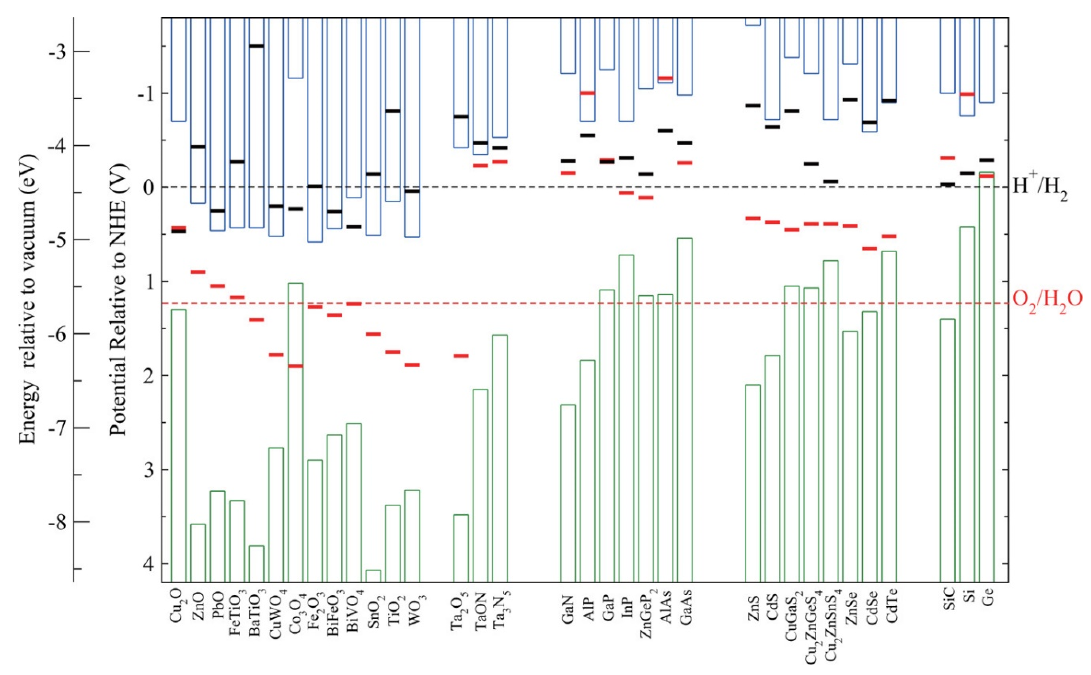
  • It presents a 2.17 eV band gap [8]. This value is low enough to have the proper energy to drive water electrolysis by visible light absorption.
  • It presents suitable bands position, allowing both the HER and the OER [9] (see below).
  • It is made of abundant and low-cost elements.
  • It is non-toxic, allowing for easier industrialization. This is an advantage if compared to other semiconductors for PEC-WS containing As, Cd and other toxic metals.
  • It can be easily and reproducibly synthetized by several methods, including electrodeposition.
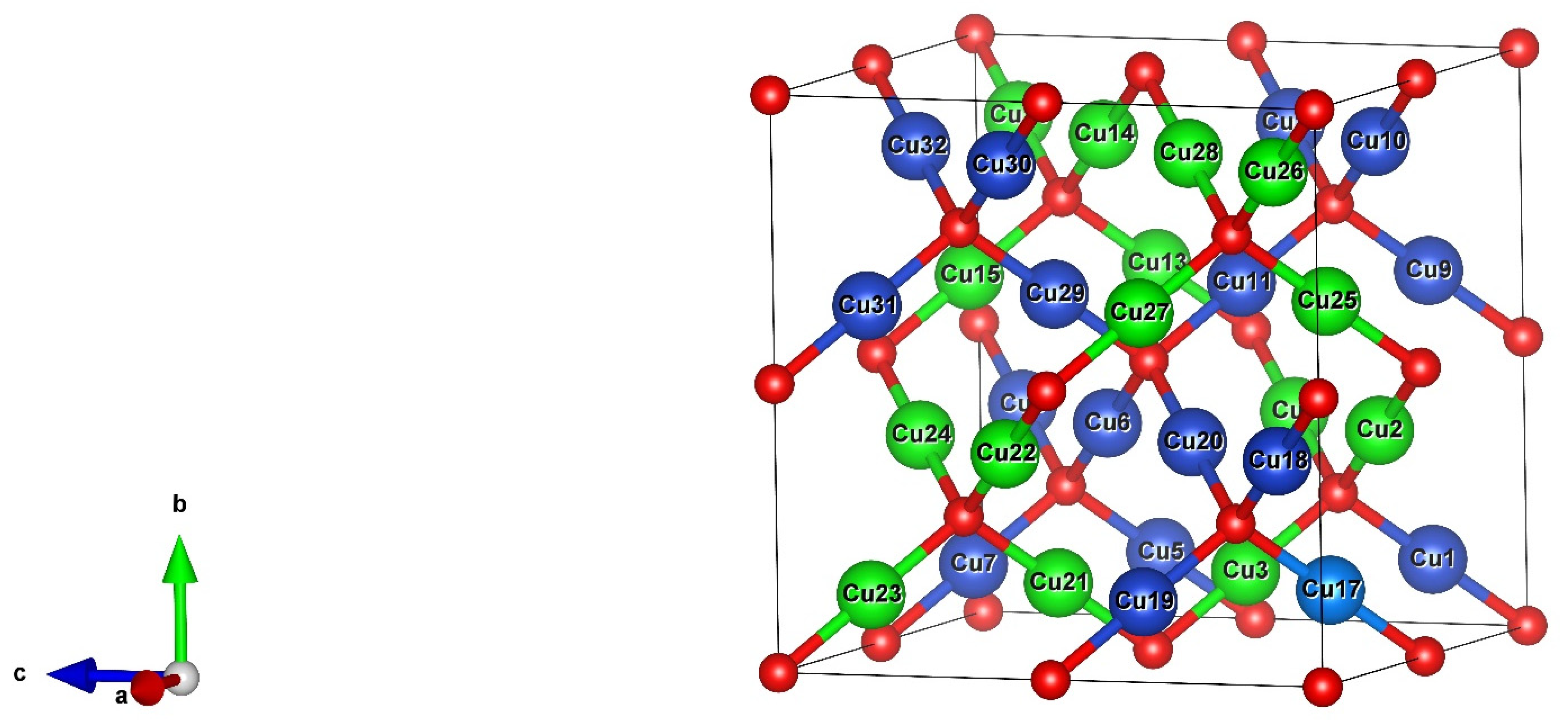
As anticipated, the bands position in Cu2O satisfies the above mentioned requirements, having a conduction band (CB) edge potential, Ec, of about −1.16 V, far above the energy corresponding to the H+/H2 couple (−0.65 V) and Ev (about +1.0 V) slightly higher than the water oxidation potential (+0.82 V) at pH = 7 [10,11].
Although Cu2O is the most promising Cu-based semiconductor, the corresponding Cu(II) oxide, cupric oxide—CuO, often co-exists with Cu2O being co-synthetized during the preparation of Cu-based photoelectrodes. Most of this manuscript will deal with the preparation, the properties tuning and the activity of Cu2O-based materials. However, it is worth spending a paragraph on CuO as well.
CuO physicochemical properties and its activity towards PEC water splitting have been very recently discussed in a dedicated review [12]. However, it is worth to summarize the main properties of CuO, because of its relevance in the topic discussed in the present work and for the frequent co-existence of Cu2O and CuO in promising photocathodes.
Like Cu2O, CuO is a p-type semiconductor (due to Cu vacancies), its structure is monoclinic, space group C2/c [13], and absorbs visible light thanks to a bang gap of about 1.7 eV [14]. CuO is more conductive than Cu2O [15]. However, n-CuO can be also synthetized [16].
CuO is a promising photoactive material, particularly for the degradation of organic pollutants, while it possesses synergistic effects when coupled with Cu2O for CO2 reduction reaction and for water splitting. In particular, CuO has been often proposed as an overlayer for Cu2O to promote electron transport towards the electrolyte, thus reducing the probability of charge recombination and increasing the lifetime. When used as a photocathode, this combination lead to impressive photocurrents up to −19.12 mA cm−2 at −1 V versus RHE [17]. Cu2O/CuO systems have an extended absorption spectra compared to pure Cu2O: While the latter have an absorption edge at about 600 nm, the former have a stronger absorption in the visible region—up to near-infrared (NIR), whose edge is at about 900 nm, due to the low band gap energy of CuO [18].
The activity of this system can be enhanced by partially reducing it by hydrogenation, leading to the formation of a thin layer of Cu(OH)2 [19], or by deposition of a carbon-based film to reduce charge recombination and promote charge transport [20].
Interestingly, a CuO/Cu2O composite can be formed starting from pure CuO and partially reducing it under operative conditions. This material retains a good photocurrent for 6 h at 0.35 V (RHE) [21].
A similar procedure carried out without the FTO (fluorine doped tin oxide coated glass) support, lead to a CuI/CuO core/shell powder that show both photocathodic and photoanodic properties with high faradaic efficiencies in the first case [22]. Interestingly, thanks to the different pH dependence of the band edges of the two component, the electronic features of this material become pH-tunable [23].
In the following, other examples of the use of photoactive CuO will be revealed.

2.1. Cu2O

Cu2O crystals have the so-called cuprite structure, a cubic Bravais lattice with the symmetry of the 224th space group (O4h, Pn3m). This structure is limited to few other compounds such as Cd(CN)2, Ag2O, Zn(CN)2, and Pb2O. Inside the unit cell the oxygen ions are located on a bcc sub-lattice, while copper ions on a fcc sub-lattice. Inside the cell, the copper ions are on the vertices of an oxygen tetrahedron and they are two-fold coordinated with the oxygen ions (D3d site symmetry), whereas the oxygen ions are fourfold coordinated with copper (Td site symmetry) [24,25].
Two interpenetrating sub-lattices compose the cell lattice in which each oxygen is tetrahedrally surrounded by four copper atoms and each copper is directly connected with 2 oxygen atoms in a linear configuration [26]. The spontaneous formation of Cu vacancies inside the lattice that creates holes in the valence band (VB) is the source of conduction.
Figure 2 shows the 2 × 2 × 2 supercell with the two interpenetrating sub-lattices (one in blue and one in green).
Figure 2. VESTA representation of a Cu32O16 supercell. Oxygen atoms are in red while the Cu atoms of the Table 1. Provides the lattice constant and the crystal structure. A transformation of Cu2O from the cuprite to a hexagonal structure occurs at the high pressure of 10 GPa (a = 4.18 Å). This hexagonal structure changes in the pressure range from 13 to 18 GPa into another hexagonal one, with CdCl2 type structure. Up to 24 GPa, the highest pressure studied, no decomposition of Cu2O into Cu and CuO was observed. Anyway, the only structure here considered is the one stable at atmospheric pressure.
Molecules 26 07271 g002
It is important to note that the reported values are almost temperature independent, as Cu2O is characterized by a very small expansion coefficient (changes in the lattice constants are less than 0.5% from 0 to 600 K). However, Cu2O is characterized by a negative thermal expansion below 300 K [27]. In Table 2 are listed the main Cu2O parameters.
Table 1. Tabulated lattice parameters for Cu2O obtained by XRD. Data from [28], with the permission from the American Physical Society.
Lattice ParametersValuesUnits
Lattice constant “a”4.27Å
Cu-O bond length1.85Å
O-O bond length3.68Å
Cu-Cu bond length3.02Å
Figure 3 shows a Pourbarix diagram of Cu calculated using the Medusa® software (https://www.kth.se/che/medusa/, accessed on 16 September 2021). Here is possible to identify the thermodynamic range of stability (in terms of pH and potential) for the different species. From the diagram it is possible to notice the narrow region of stability of the Cu2O, while the CuO oxide is much more stable from pH above 5. The water stability range is, as usual, represented between the dotted lines at 0 and 1.23 V at pH 0. The concentration of Cu2+ here considered was the one present in the electrodeposition bath of Cu2O, discussed later as one of the most promising preparation routes.
The optical properties of a material are of extreme importance in photo-electrochemistry and thus PEC-WS applications. Cu2O has a direct band gap of 2.17 eV [8]. However, according to the absorption spectrum (Figure 4 [18]), it starts to only absorb the light above approximately 2.4−2.5 eV (500—520 nm). This energy is related to the dipole allowed transition between the higher valence band and the second lower CB [30]. Figure 4 also shows the absorption spectra of CuO and of a Cu2O/CuO system: the former having a wider absorption range thanks to the lower BG, the latter combining the optical properties of the two oxides.
Cu2O band gap was considered as related to d10-d10 interactions between the Cu 3d states of adjacent Cu ions [31,32,33]. Recent studies showed that these interactions do not exist [34]. Instead, thanks to a combined analysis of the density overlap region indicators (DORIs), crystal overlap Hamilton population (COHP) and the density of states (DOS), it was demonstrated that the chemical bonding in Cu2O is mainly characterized by covalent bonding. Within this configuration the electrons are delocalized over Cu-O-Cu moieties through two-electron and three-center bonds [34]. Following this analysis, both the CB and VB edges are determined by covalent σ* antibonding bonds between Cu 3d4sp and O 2sp3 states.
The delocalized nature of the multicenter bond determining the VB and CB edges can be exploited to manipulate the band gap both through inducing strain onto the Cu2O lattice [34], and by doping with inert same-valent ions in high concentrations [35]. Both effects have been observed in quantum chemical modeling studies. Imposing, for example, tensile strain onto the lattice of Cu2O results in a weakening of the Cu-O bond and thus in a reduced energy gap between bonding, non-bonding and anti-bonding states. This in turn translates into a reduced band gap (Figure 5). The opposite effect is observed when compressing cuprite by up to −3%. increasing the tensile strain further, Cu2O starts to show an anomalous behavior, in the sense that the band gap starts to decrease again. This was associated with the presence of delocalized Cu 4sp, which starts to dominate the CB edge.
Doping Cu2O with high concentrations of inert group I metals, such as Li or Na, on the other hand, disrupts the delocalized two-electron and three-center bonding network and effectively localizes the electrons in a confined space. This in turn converts into an increased band gap (Figure 6) [35].
Decreasing the concentration, thus increasing the space in which the electrons are delocalized, reverts this effect. Similarly, doping with Ag and Au ions does not affect the band gap to a significant amount. This is not surprising when considering that these ions can contribute to the two-electron and three-center bonding network.

2.1.1. Preparation Methods

Different preparation methods are reported in literature to produce a valid Cu2O layer for photo-application. The most valid ones are reported below.
Thermal oxidation of metals is a widely used method for the synthesis of high-quality oxides. In this case, the procedure involves the oxidation of a high purity copper foil from a few minutes up to several hours depending on the required final thickness of the Cu2O layer. Temperatures are in the range between 1000–1500 °C under pure oxygen atmosphere or mixed gas atmosphere (like Ar + O2) [36]. The obtained Cu2O is polycrystalline with different grain structures according to the chosen experimental conditions. During the thermal process two reactions can occur:
4 Cu + O 2   2 Cu 2 O  
2 Cu 2 O + O 2   4 CuO  
The formation of a mixture of two major oxides, CuO and Cu2O, is always possible and thus the partial pressure of oxygen during the annealing process must be strictly controlled. The formation of Cu2O occurs first while longer oxidation time are needed for CuO to appear [37]. An alternative method starts from a Cu foil that is converted in Cu(OH)2 by the use of 0.125 M (NH4)2S2O8 followed by thermal reduction. Nanocorals of Cu2O [38] or nanosized Cu2O are obtained if the oxidation is performed in KOH and a dehydration step is performed [39].
One of the most attractive methods for large scale and high-quality production of Cu2O is electrodeposition. The advantages of this method are that it is cheap, can easily work on different substrates and allows the tuning of the material properties and morphology working with parameters like: The applied potential, the current, the temperature, and the pH of the bath [40]. The first electrochemical synthesis of Cu2O was presented by Stareck [41]. Successively, many other authors developed different synthetic procedures using different copper precursors electrolytes and electrochemical parameters [42,43,44].
Mao et al. used a solution of 0.01 M Cu(NO3)2 + 0.1 M NH4NO3 with a current density of 0.5 mAcm−2 for 60 min at 313 K. The resulting photocurrent was quite low [45]. Wan et al., using 0.02 M Cu(Ac)2 and 0.1 M CH3COONa aqueous solution with 1.5 mM KCl, were able to control the shape of the grains with pH modulation, but the conductivity of the so obtained material was n-type [40]. Zhao et al. performed electrochemical oxidation of a Cu foil in a solution of 280 gL−1 NaCl and 0.1 g L−1 Na2Cr2O7, with pH adjusted between 8 and 12 by 1.0 M NaOH [46]. They show a net decrease in the band gap value probably as a result in the particles morphology [46].
To the best of our knowledge, the highest results in terms of photocurrent were obtained using a CuSO4 solution with lactic acid and the pH shifted to basic value (usually 12) [47,48,49,50]. This is a development of the recipe derived from Golden et al. [48,49,50,51]. The photocurrent obtained with this recipe largely changes according to the specific publication. For example, Nian et al. [52] obtained a maximum photocurrent of −0.025 mAcm−2 on FTO, the Graetzel group [48,49] obtained values as high as 2 mAcm−1, while Visibile et al. reached 1.6 mAcm−1 tuning the properties of the metallic underlayer below the semiconductor [53]. This highlights the extreme importance of controlling every parameter in the deposition with high accuracy.
PEC-WS’s performances of systems fabricated with this method are nowadays one of the most efficient and leading to the highest photocurrents. This method guarantees that the semiconductor layer is very homogenous and has highly tunable properties. For example, it is possible to control the oxide morphology and the particle’s size [54,55] by simply varying selected bath conditions like potential, temperature and pH [54,55]. It is also important to cite the controlled oxidation of a copper foil in different solutions [56,57]. The result obtained with this method in terms of photocurrent falls behind the one previously described.
Other synthetic procedures includes reduction of copper-amine complex solution with glucose under microwaves irradiation [58], the use of different surfactants [59,60,61,62,63,64] and micelles [65] mostly to control the morphology of the particles. Using these procedure, Cu2O nanowires and nanocrystals [66] with cubic [67,68,69], cuboctahedral, truncated octahedral, octahedral [70], and multipod structures [71] have been prepared [72]. Surfactant free synthesis have also been developed to reduce interferences from these surfactants [73,74,75]. Solvothermal [76,77] and sol-gel [78] methods [76,77] have also been tested. Wet chemical routes [79,80], thermal evaporation [81,82], chemical vapor deposition [83], sonochemical synthesis [84], hydrothermal [85,86,87] and electroless [88] methods are only few of the other alternatives methods for the synthesis of this semiconductor. Another interesting technique for the preparation of thin films is sputtering. This preparation route allow high homogeneity, low cost and easy synthesis [89]. With this synthesis there is usually no available data about the produced photocurrents.

2.1.2. Cu2O Advantages and Disadvantages for PEC-WS System

In a PEC-WS system, electrochemically deposited Cu2O is a preferential choice because:
  • Cu2O has a 2.17 eV band gap. The value is high enough to have the proper energy for hydrogen evolution, but not so high, thus the material can absorb in the visible range of light. Compared to material like TiO2, able to absorb only in the UV due to their large BG (~3 eV), this is a great advantage.
  • Cu2O has a proper bands position for both HER and oxygen evolution reaction OER. In most scenarios the material is used as a photocathode.
  • Cu2O is a low-cost semiconductor that originate from abundant precursors. This allow a sustainable scale-up of the electrode material production.
  • Cu2O is non-toxic. Compared to other semiconductors for PEC-WS containing As, Cd and other toxic metals, this is of great interest from the environmental point of view.
  • Electrochemical synthesis allows wide control over different parameters, being able to obtain high-performance electrodes.
  • Electrodeposition is a cheap and fast method for the preparation of a large amount of electrodes.
Looking in detail at the Cu2O band position in Figure 7, we can see that is one of the few materials with a narrow band gap still able to achieve both the HER and the OER (CB more negative than H2/H2O redox potential and VB more positive than O2/H2O redox potential).
From the same picture, the main disadvantage of this material is also evident. The redox potentials for material reduction/oxidation lie inside the band gap. Thus Cu2O can undergo the photodegradation process, where, in this case, both holes and electrons can interact with the material provoking, respectively, oxidation and/or reduction.
To extend material lifetime towards photodegradation and enhance the material’s performances, two different approaches have been used in the literature: doping and protection with an overlayer.
Creation of a protective heterojunction is instead a way of protecting Cu2O from the photodegradation mechanism. The idea behind is to use an overlayer able to quickly remove electrons from Cu2O thanks to the redox cascade principle before they react with the material itself.

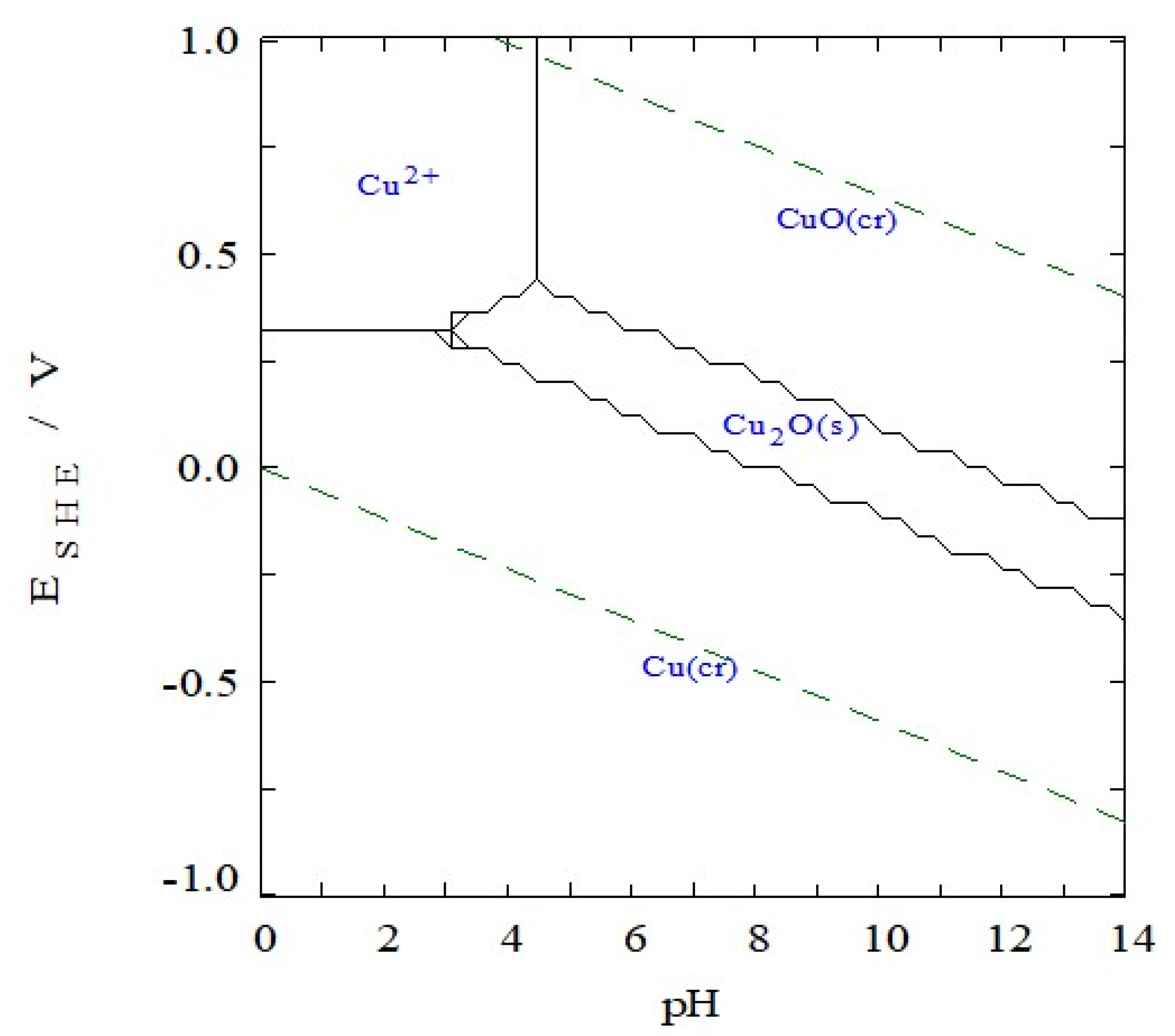
2.1.3. Stability of the Semiconductor

Photodegradation is the worst of the many undesired processes occurring after electron-hole couple creation because it reduces the material activity with time. This problem is widely common in semiconductors for PEC-WS.
There are four different levels of stability for a semiconductor according to the VB and CB levels, with respect to the redox potentials of the material (Figure 8):
(a) Thermodynamic stability: The redox potentials of anodic and cathodic decomposition reactions (Ep, En respectively) are more positive (less negative) and more negative (less positive) than the VB and CB edges, respectively.
(b) Anodic and cathodic degradations: Both redox potentials lie inside the BG. The material can be degraded by electrons reduction and holes oxidation.
(c) Anodic degradation: The CB edge potential is more positive (less negative) than that redox potential so the semiconductor is stable from cathodic degradation. Anodic corrosion by holes still affect the material by self-oxidation.
(d) Cathodic degradation: Holes do not affect the material but the high energy electrons excited in the CB can perform undesired material reduction.
The photodegradation is in competition with the desired processes of surface electrons transfer. The favored reaction is the one with less energy required but also kinetics plays an important role and thus it is not always easy to predict the final behavior of a material [9]. Other important parameters influencing the stability are the chosen electrolyte and its concentration and pH, temperature, impurity levels and other setup parameters (e.g., stirring that can affect the rate of electrode processes).

2.1.4. Vacancies Formation

The Cu+ ion external electronic structure is 3d104s0, with the 4s orbitals only a little higher in energy than the 3d levels. The Cu 3d levels form the VB of Cu2O and the empty Cu 4s levels form the CB [90,91]. This is different from most metal oxides, which have O 2p states at the top of the valence band. From DOS analysis, it was demonstrated that Cu2O has a direct gap at the center of the Brillouin zone (Γ point) [92].
Kleinmann et al., in their DOS analysis Figure 9 [93], have the typical underestimated BG of LDA methods (Figure 9 and Figure 10). Figure 10 instead shows the BG calculated with hybrid functional, a result much closer to the real one with the different contribute of d-orbitals in the valence and conduction band. The real measured energy gap is Eg = 2.1720 eV at 4.2 K, obtained as the limit of the yellow exciton series and it decreases with temperature [93]. Using a range separated hybrid functional (HSE06), we recently found a BG of 1.95 eV [34].
As mentioned earlier, one of the key parameters for PEC-WS materials is their band positions with respect to the water oxidation and reduction potentials. Water reduction and oxidation potentials must fall within the valence band edge (Ev) and conduction band edge (Ec) for the reaction to be thermodynamically favorable. The closer the Ec energy to the vacuum level, the stronger the reducing power. In the same way, the lower Ev, the higher the oxidizing driving force. The bands alignment of Cu2O satisfies all the above mentioned requirements.
Conductivity for Cu2O comes from copper vacancies that create acceptor states within the BG at energy values of 0.3−0.5 eV above the top of the VB. Copper vacancies (VCu’s) can reach concentrations up to 1020 cm−3, but the free holes’ concentration at 25 °C is usually only around 1018 cm−3 because not all the vacancies are ionized. The formation enthalpies of the defects suggest that many parameters like the O2 partial pressure, temperature, and Fermi energy can largely modify their concentration. The annealing temperature can, moreover, increase the minority carrier lifetime up to one order of magnitude [94,95,96].
The formation of a Cu vacancy occurs easily and spontaneously as the computed energy is 0.38 eV [90], a quite low value if compared to similar materials. Once one vacancy is already present, the formation energy for the next one changes according to the reciprocal position of the two vacancies. Nolan et al. computed the different energies to found the most favorable position that is on a different Cu2O network (Table 3) [90].
The most stable configuration for dopant and Cu vacancy is the one where the Cu vacancies are clustered (i.e., separated by the internetwork Cu-Cu nearest neighbor distance, with one vacancy on the same Cu2O network as the dopant and the second vacancy in the other Cu2O network). When the number of vacancies is increased to three, two of the three Cu vacancies are in the same Cu2O network. Similar for four Cu vacancies, where three of them are found in the same Cu2O network, and so on.
A neutral oxygen vacancy, able to add electrons to the system, could compensate the holes but taking away a single neutral oxygen atom tetrahedrally coordinated to a Cu atom requires 3.08 eV, much more with respect to a neutral copper vacancy. Other combinations of Cu and oxygen vacancies present even higher formation energies. In other words, the Cu vacancies compensation by formation of oxygen vacancies is not favored process. Moreover, another study suggests that hole traps formation is not linked with Cu vacancy, avoiding any negative impact on the conductivity [97].

2.2. Doped Copper Oxides

Bulk doping with ions (metal or non-metal) is a simple method of semiconductor photosensitization (shifting the absorption edge towards lower energy light) and improvement of photocatalytic activity. Dopant ions provide an additional energy level (donor or acceptor levels) within the band gap of the semiconductor [98]. Light-induced electron excitation from the valence band to the acceptor level, or from the donor level to the CB, requires a lower photon energy compared with the excitation of bare semiconductor. Moreover, a dopant ion can act also as a charge trap, leading to prolongation of the lifetime of the charge carriers and towards an enhancement of the photocatalytic activity. On the other hand, doping leads also to several negative effects: (i) decrease of carrier mobility owing to the formation of the strongly localized additional states within the band gap, (ii) increase of the rate of photogenerated charges recombination [99,100]. Copper oxides, as semiconductors with a narrow band gap, are active in visible light and, therefore, the purpose of the doping is not associated with sensitization to visible light, as is usually the case of wide band semiconductors (e.g., TiO2, ZnS).
Doping is the addition of impurities into the material lattice with the aim of modifying the band gap and the bands position. As a result of this, the fraction of light absorbed by the semiconductor as well as carriers’ number and mobility can be increased. Moreover, doping might include some strain in the material lattice as a result of the different ionic sizes of the dopant. This strain might result in a modified band gap, as suggested by Visibile et al. using DFT calculations [34].
Cu2O presents a spontaneous p-type conductivity and it is also a compensated material where both intrinsic acceptors and, in smaller number, donors co-exist. The compensation ratio NA/ND, (the acceptor concentration over the donor concentration), is usually just slightly larger than 1 and always lower than 10. A similar condition found in other semiconductor has been explained with the self-compensation mechanism [101]. The higher is the number of donor impurities inserted in the material, the more the acceptors formation energy is reduced; in this way, donors are always less than acceptors. The nature of the compensating donor is still controversial (simple candidates could be oxygen vacancies) and also their identification as intrinsic defects is not assessed. Many authors claim n-type doping to be impossible because of the self-compensation mechanism, others claim to be able to obtain an n-type behavior, for example, with Cl-doping [102,103,104,105].
Cation doping changes the material crystal structure of two interpenetrated Cu-O networks kept together by non-bonding Cu-Cu interactions. The Cu2O BG can be increased or decreased with the use of the appropriate dopant, because any change is the sum of different mechanisms:
(i)
The size of the dopant cation. It affects the Cu-Cu interactions in the Cu2O host lattice (e.g., Sn2+ increases the Cu-Cu distances because of its larger ionic radius thus increasing the BG by reducing the metal character of the material). In general dopants with ionic radii larger than Cu+ (like Ba2+, Sn2+, Cd2+, In3+, La3+, Ce4+ etc.) produce strong structural distortions around the dopant site. Dopants with ionic radii smaller than Cu+, such as Al3+, Ga3+, Ti4+, and Cr4+, show almost no structural distortions.
(ii)
The alignment of the dopant electronic states with those in the VB or CB of Cu2O (e.g., dopants like In3+ (larger than Cu+) or Al3+ (smaller than Cu+) cause a decrease of the BG because of unoccupied 3s states with much lower energies than the Cu 4s orbitals).
(iii)
The introduction of dopant ionic states within the gap with the possible formation of an intermediate band (IB).
(iv)
Charge localization through insertion of insulating ions such as Li+ or Na+. This typically results in an increased BG.
The sum of all these effects affects the final material behavior. The isovalent doping of Cu2O using Ag+ or Au+, for example, produces little structural distortions into the Cu2O lattice and BG is not affected. The hole mobility is only slightly affected because the d10 levels of Au+ and Ag+ are too low in energy to have a strong interaction with the d10 levels of Cu+ [97].
Regarding the structural distortions introduced by cations doping in Cu2O, the d10-d10 interactions between Cu atoms are of paramount importance in determining the BG and the width of the VB. When the d10d10 interactions are suppressed, Eg is indeed increased. This results shows that the physical properties are related not only to 2D interactions but also on its global spatial arrangement. Thus Cu-Cu 3D interactions must be improved to reduce the BG [32,106].
Doping with cations larger than Cu+ increases the band gap, while maintaining the cubic structure because it distorts the crystallographic lattice and thus decreases 3D Cu-Cu interactions resulting in a BG increase. The distortions induced by the dopant in the Cu2O lattice depend obviously on the size of the dopant. In the case of early transition metals (TMs), the TM-Cu bond length (dN-N) is shorter than the Cu-Cu bonds in the pure Cu2O host. This phenomenon has been noted in several works. The explanation is that the deviation from the d10 configuration results in stronger TM-Cu bonds [32,33].
Cu+ in Cu2O behaves as a soft Lewis acid, with metallic Cu-Cu interactions creating high-lying VB states and low-lying CB states, resulting in a higher conductivity and lower transparency with respect to the oxides of harder Lewis acids (e.g., Na2O). Thus, as suggested by literature [31], the use of cations from hard Lewis acid tends to increase the band gap, while using cations from soft Lewis acid leads to a reduction. This strongly depends on the purpose for the Cu2O preparation. An electrode for PEC-WS should present a quite low BG, instead a p-type semiconductor for transparent conductive oxide (TCO) [107] should possess a quite wide BG. The latter are used as transparent electrodes in flat panel displays and in solar conversion devices. Examples of TCO are indium tin oxide (ITO), ZnO or FTO. For their preparation the synthesis of a semiconductor with large band gap and still high conductivity is mandatory [32]. Nowadays, all TCO are n-type semiconductors, and the development of a hole-conducting material (p-type) like Sr:Cu2O [107] could generate new applications for this kind of material, like functional windows able to transmit visible light but at the same time to generate current due to the absorption of UV photons. The BG tunability is, thus, a great advantage of Cu2O.
In Cu2O, aliovalent dopants compensation is achieved by forming Cu vacancies. For a dopant of oxidation state n+, (n − 1) Cu vacancies are needed to compensate, the subsequent (n-th) Cu vacancy is used to dope the system p-type. Aliovalent cations can thus be used to increase the number of vacancies. The values of vacancy formation energies with different dopant cations are reported in Table 4 with data coming from Nolan et al. [31].
In the column headed E n 1 v a c is shown the formation energy for the first Cu vacancy compensating for dopant with oxidation state Mn+; in the column headed E n v a c is presented the formation energy for the Cu vacancy that creates the p-type for dopant with oxidation state Mn+.
H and passivation: Tabuchi et al. [108], with an exposure time of 30 min, pH2 = 1 m Torr at a temperature Tsub = 300 °C [108], succeeded to reduce the carriers concentration from 1.7 × 10¹⁶ to 2 × 1015 cm−3 and to increase the mobility from 5.3 to 28.9 cm2/(V s). Thus hydrogen has the ability to passivate acceptors. According to the authors, mobility increases by the lower effect of ionic impurity scattering due to the lower carrier concentration and then by the passivation of the dangling bonds at the grain boundaries. Passivation of non-radiative recombination centers can be also obtained by cyanide treatment with an increased holes density [109].
Alkaline Metals: Alkaline doping mostly ends in reduction of the direct band gap moving the acceptor level edge to the maximum of the VB. Moreover, AFM showed a carrier density and electrical conductivity increase as well as a reduction in the photocurrent with the dopant ion size. Our computations indicate that alkaline metal doping affects the BG through a combination of geometric and electronic effects. The formers are the result of differences in the ion size and effect Cu2O in an identical manner than simply straining the oxide whereas the latter are a result of the destruction of the semiconducting network of two-electron three-center bonds spanned by the Cu-O-Cu bonding network. Both effects only notably affect the oxide at very high concentrations [35]. On the other hand, Caballero-Briones et al. claimed that the main effect of the alkaline substitution of copper atoms is the polarization of O states, with a reduction in the insulating gap and splitting of the density of states just below the Fermi level [110]. In particular, with Na the resistivity is decreased from 1.2 × 10⁶ to 330 Ωcm, and the carrier concentration rises from 5.1 × 10¹⁴ to 1.7 × 10¹⁸. A small reduction of the BG (from 2.19 to 2.04 eV) due to the creation of an impurity acceptor level above the valence band was recorded [111,112,113].
Chlorine: Results on this material shows a conductivity about one order of magnitude greater than the undoped material. Carriers concentration’s (holes) measurements as a function of temperature proved chlorine to be a donor, substituting the oxygen, and an acceptor as well, sitting in an interstitial position [105].
Nitrogen: It slightly opens the band gap with the formation of an intermediate band (IB) at about 0.9 eV from the VB. The IB is mostly composed by hybridization between the N-2p states and the Cu-3d states. According to some authors, in this doping, nitrogen atoms substitute oxygen ones behaving as a p-type dopant [114], but other papers are in disagreement, considering it too difficult to substitute O with N because of the larger radius of nitrogen [115]. Anyway all the studies found improvements in the absorption coefficient spectra [116,117] as a result of the presence of an intermediate band (IB).
Zinc and indium: According to different authors, the Zn-doping can reduce the lattice constant of Cu2O, giving an increase of the BG when Zn act as a donor impurity [118,119]. Some authors found that Zn-doped Cu2O has a larger resistivity than the undoped one [120], while others found an improved carrier concentration and charge transfer, despite an extremely low photocurrent [121]. Heng et al. [122], noticed a shape evolution of the Zn-doped Cu2O microcrystals. In particular, increasing the relative concentrations of the Zn precursor leads to a decrease in the numbers of facets. A small increase in the band gap with the increase in Zn concentration was recorded too. Indium acts as a donor impurity in Cu2O [120] by increasing the lattice constant and the band gap. In some cases this can lead to the formation of n-doped Cu2O [120].
Silicon: Si is usually coordinated with four oxygen atoms, instead of two like copper. Therefore, Si acts probably not as a substitutional impurity but creating SiO2 inclusions [123]. This leads to a lowest resistivity of 12 Ω cm and a Hall mobility of about 10 cm2/(V s). No information on photocurrents were given.
Silver: Ag-doping generates minimal changes in the band gap and band gap energies. Improved conductivity and photocurrent density (up to four times) with respect to undoped samples were recorded [124]. Ag in Cu2O can, owing to its chemical similarity to Cu and the presence of d-orbitals, directly replace Cu in the structure without significantly influencing the bonding situation. Computations indicate that the bonding situation is somewhat more covalent, which allows for a stronger delocalization, thus could explain the experimentally observed higher conductivity and higher charge carrier generation, which in turn provides a greater photo-response [35]. High dopant concentration decreases the performances because of recombination centers that inhibit the increased charge separation efficiency [124].
Iron: Fe-doping shows a reduced experimental BG from 2.5 to 2.2 eV with enhanced photocurrent at minimum dopant concentration (2%). Higher concentrations generate more defects that, as recombination centers, reduce the charge separation. The recorded improved conductivity could be also due to the presence of Fe 3d states in the doped sample [125,126].
Gold: Doping with gold produces only a minimal change in the optical absorption edge (−1.6% of the undoped value). Gold is also helpful for improving the transmissions of photoelectron and vacancy thanks to the formation of an impurity level, which can enhance the visible absorption, and reduce the absorption efficiency of UV light [127]. Au has been found to reduce recombination phenomenon too. Computations indicate that the electronic structure of Au-doped Cu2O is affected in an almost identical manner to what has been observed for Ag [35].
Magnesium: Mg-doped Cu2O gives a great boost to the conductivity. The doped thin films with morphology changes showed an electrical resistivity decrease from 202 to 6.6 Ωcm, due to the increase of charge-carrier density. The BG increases a little to 2.4 eV compared to intrinsic cuprous oxide, but, on the other hand, the charge carrier density increases from 4.5 × 10¹⁵ up to 8.1 × 1017 cm−3 with increasing Mg content from 0% to 17% due to the enhanced formation of copper vacancies. These two properties combined lead to a general decrease of resistivity [128]. Other authors claimed that the similar ionic radius of Mg with respect to Cu, together with its d5 configuration, should make Cu2O less prone to form trap states [129].
Strontium: Strontium doping induces a significant improvement of the electrical properties, with a thin film resistivity reduced down to 1.2 Ωcm at 25 °C with a strontium content of 5–7%. However, at higher strontium concentrations, the resistivity increases again even after annealing. The room temperature densities of the free hole lies in the range of 1.2 × 10¹⁵ to 2.8 × 1017 cm−3, depending on the Sr content and on the post-deposition annealing [130].
Other authors find that an increase in Sr content decreases resistivity from 106 to 102 Ωcm for film with 5–6% of Sr. Unlike Nolan’s calculation [90], no increase of the band gap was recorded in the experiments while morphology is affected by Sr content indeed [131].
Manganese and Nickel: Mn-doping results is an increased resistivity at room temperature for the doped sample [132]. In another case, the resistivity of the doped samples was lowered by a factor of 2 with respect to the undoped ones [133]. Undesired results were found also for Ni-doped Cu2O. When the Ni atoms enter the interstitial sites they produce scattering centers of the neutral impurity, resulting in low mobility. The mobility in Ni-doped films monotonically increased with increasing deposition temperature, while the mobility in undoped films decreased [134]. Thus Ni impurities do not affect the carrier concentration but only the mobility.
Single cationic doping with the generation of acceptor states in the band gap is not the only possibility when talking about Cu2O doping. Indeed, these states could behave like recombination centers reducing the efficiency of the photocatalyst. Instead of mono-doping, anionic and cationic co-doping could improve the properties of the material. This is also of help in case of poor dopant solubility. The simultaneous incorporation of p-type and n-type dopants (compensated co-doping) will lower their formation energy [135].
The calculated defect formation energy shows that co-doping is energetically more favorable than mono-doping due to Coulomb interactions and charge compensation effects. Recent results were reported with TiO2 [136], ZnS, Bi2WO6 [137,138] and of course on Cu2O [10] with DFT calculations. On Cu2O, the best combination found was composed by Sn + B doping, and this leads to a reduction of the forbidden band gap and an increased optical absorption.
Another interesting property of the doped system is the introduction of an intermediate band (IB) inside the BG of the semiconductor because of the energetic level of the dopant. These systems are called intermediate band solar cells (IBSCs) (Figure 11). Firstly discovered by Luque [139,140] in 1997, they are still studied today because of their great advantages [141,142,143]. The IB acts as a steppingstone for electrons coming from VB. In this way, electrons can be excited also by photons, having less energy than the BG but at least the energy between IB-CB and IB-VB. With this trick the total carriers generation increase and the light absorption is expanded significantly [144,145,146].
On Cu2O systems Malerba et al. [148] and other authors [119,121,149] obtained interesting results with N-doped Cu2O both from computational and experimental points of view.
A new absorption peak below the BG with a red-shift of the absorption band edge is visible in Figure 12 from the paper of Ping et al. [116]. The higher number of useful photons can be used for the electron-hole pair generation and thus improve the performances of the material. A schematic representation of the mechanism is given in Figure 13.
To obtain an efficient IB, some requirements have to be fulfilled [139,150,151,152,153]:
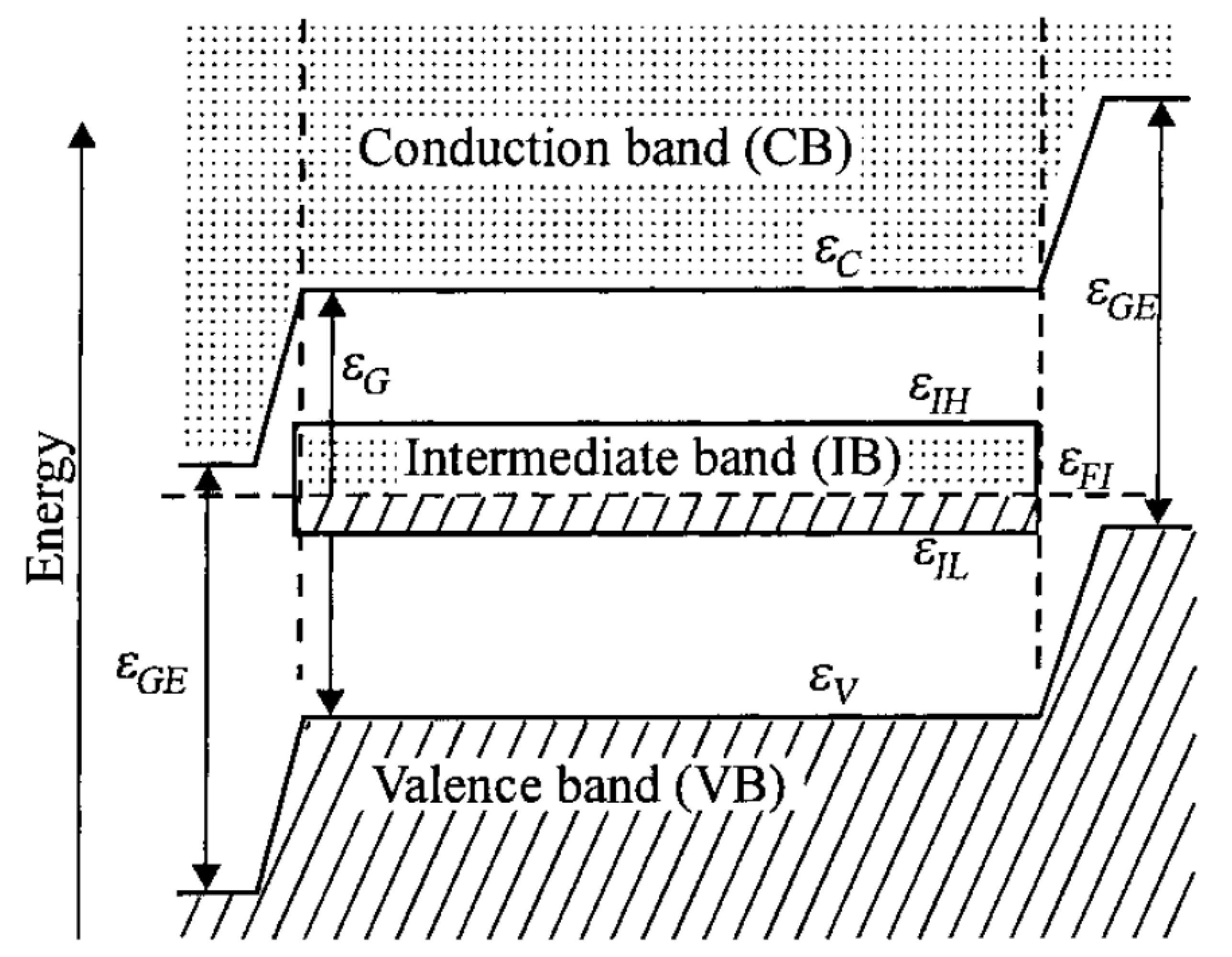
  • To have strong light absorption for transition to and from IB, it has to be half-filled and lie on the Fermi level [147].
  • Must be clearly separated both from VB and CB to avoid recombination.
  • Split the original BG in two sub-band gaps of approximatively the same width to maximize the use of photons.
  • Should not be a center for non-radiative recombination.
  • It must have small dispersion and must not be a discrete level.

2.3. Ternary Copper Oxides

Delafossites are an example of ternary oxides, which have a quasi-two-dimensional layered superlattice structure. In this structure, the linear O–A–O dumbbell layers and oblique BO6 octahedra layers are alternately arranged [154]. Delafossite materials based on copper (CuMO2; where M = Fe, Rh, Cr, Al, Ga) has attracted great attention as a possible cathodic photomaterials for solar fuel production because of the small band gap energy, high onset potential and good stability in aqueous electrolytes. Crucial electronic properties of copper-based ternary oxides are summarized in Table 5. On the other hand, poor charge transport properties yield in a low efficiency of photoelectrochemical H2 evolution [149]. Copper-iron oxide is one of the few oxides that naturally displays p-type conductivity but, unlike Cu2O, CuFeO2 is stable under reductive conditions [155]. The conduction band of CuFeO2, located at around −0.4 V vs RHE, is suitable to reduce water to hydrogen under light. The most commonly used synthesis methodology consists of the solid-state reaction between iron and copper oxides in oxygen-free atmosphere at 800 °C. In order to improve the photoactivity of delafossite material, a unique fabrication strategy has been proposed. The CuFeO2 was prepared by hybrid microwave annealing (HMA) as a post-treatment [149]. The HMA method resulted in interstitial oxygen doping into CuFeO2 lattice to form CuFeO2+1.5δ, thereby increasing charge conductivity and improving electron-hole separation (more than four times higher photocurrent density in comparison with conventional thermal annealing). Prévot et al. proposed citrate-nitrate sol-gel method, whereby metal nitrates were mixed with citric acid, ethylene glycol and ethanol [155]. This procedure resulted in thin film obtained directly on FTO (fluorine-doped tin oxide) glass, which revealed high photocurrent densities (up to 1.4 mA cm−2), by using sacrificial electron acceptors and an advantageous photocurrent onset at +0.9 V vs RHE. This material absorbs light in a broad wavelength range—the IPCE onset being at λ = 830 nm. Further studies reported high density of surface states, which may cause Fermi level pinning at the SCLJ [156]. These surface states act as electron traps, resulting in an inversion of the depletion layer upon filling, both in the dark and light conditions, thereby promoting charge recombination at the surface.
Other promising p-type copper-based delafossite photoelectrocatalysts are: CuCrO2, CuAlO2, CuGaO2 and CuRhO2. The delafossite CuCrO2 photocatalyst can be prepared using hydrothermal and solid-state reaction methods resulting in a significantly different materials. A hydrothermal CuCrO2 sample is characterized by higher purity, lower crystallinity, smaller particle size and higher photocatalytic activity in comparison with samples prepared by a solid-state method [157]. The CuAlO2 photocathodes ware fabricated by electrodeposition of Cu2+ and Al3+ onto FTO glass, followed by thermal treatment [158]. CuAlO2 possesses suitable electronic properties for H2 evolution under solar light and exhibits a photocurrent onset potential of +0.9 V vs RHE, along with a faradaic efficiency of ca. 70% at +0.3 V, which can be significantly improved by the addition of sacrificial hole scavengers. A hydrothermal method has been applied also to prepare CuGaO2 [154]. The CuGaO2 electrode exhibits the potential for hydrogen production, long-term stability and large photocurrent density in PEC tests. The CuGaO2 electrode exhibits the potential for hydrogen production with a small overpotential (−0.1 V) and long-term stability. Bocarsly’s group described a CuRhO2 material that is a more active photomaterial in oxygenated conditions, due to O2-driven self-reparation [159]. Under irradiation, the CuRhO2 can undergo reductive deactivation, but in the presence of oxygen this regenerates the active photocatalyst again. CuRhO2 enables evolution of H2 with ca. 80% Faradaic efficiency.
A literature describes also numerous other ternary oxides characterized by relatively high activity in photocatalytic or photoelectrochemical reactions. Many of these examples are summarized in an recent review [161]. Among them there are copper (I)-based compounds (e.g., CuNbO3, Cu2Ta4O11 and Cu3VO4) and copper (II)-based oxides (e.g., CuAl2O4, CuCo2O4, CuFe2O4, CuMn2O4, CuV2O6, Cu2V2O7 and CuWO4). Furthermore, it is worth mentioning a few other materials. Berglund at al. reported CuBi2O4 photocathodes fabricated by a straightforward drop-casting method [160]. It was reported that the optical absorption of CuBi2O4 is rather weak, as they exhibit a gradual instead of sharp increase in absorption for light energies above the band gap value—this reduces the photocurrent density. Another limiting factor is poor charge carrier (mainly holes) transport, which reduces the obtainable photocurrent density of two orders of magnitude. Copper ferrite, being a p-type semiconductor, was applied as a photocathode in water splitting reaction. CuFe2O4, prepared directly on FTO glass via the sol–gel method followed thermal treatment, generated a photocurrent density of 1.82 mA cm−2 at 0.4 V vs RHE [162]. This result is significantly more encouraging than those of many other copper oxide materials. This has been associated to the reduced oxygen vacancy concentration and thus facilitated charge transport and interfacial charge transfer efficiency.

2.4. Quaternary Copper Oxides

Quaternary oxides contain copper and two other metal cations in the oxide structure. Literature shows significantly lower interest in quaternary oxides materials in comparison with ternary oxides. The Cu2BiVO6 consists of a 4:1:1 combination of Cu2O, Bi2O3 and V2O5. Cu2BiVO6 has strong visible light absorption, starting at 600 nm and band gap energy smaller than that of BiVO4 due to a mixing of the Cu-3d orbital with the V-3d conduction band of BiVO4 and to the mixed Bi-6s [163]. Under illumination, this material generates both anodic and cathodic photocurrents, attributable to water oxidation and reduction, respectively. Zhou et al. reported that another quaternary oxide, CuBiW2O8, exhibits a strong absorption of visible light and it has a promising values for mobility of photoexcited carriers compared to ternary oxides such as a BiVO4 and CuBi2O4 [164]. CuAlGaO4 is a visible-light-active materials for hydrogen photocatalytic evolution from H2S with quantum yield of 10.8% at 550 nm [165]. Further increases of quantum efficiency were achieved when CuAlGaO4 was loaded with nickel oxide. Double perovskite compounds Sr2CuWO6 and Ba2CuWO6 were investigated as photocatalysts and photoelectrocatalysts [166].

2.5. Composites of Copper Oxide with Other Semiconductors (Heterostructures)

Heterojunction occurs between two different semiconductors with suitable band gap alignment leading to the enhanced transfer of photogenerated charge carriers by reducing recombination rates of electron-holes pairs. This approach is considered as the most promising method leading to an improved photoactivity [167]. This becomes particularly important in the case of copper oxide, because of its tendency to photocorrosion. The heterojunction materials can be classified into three different types based on the band structure (Figure 14):
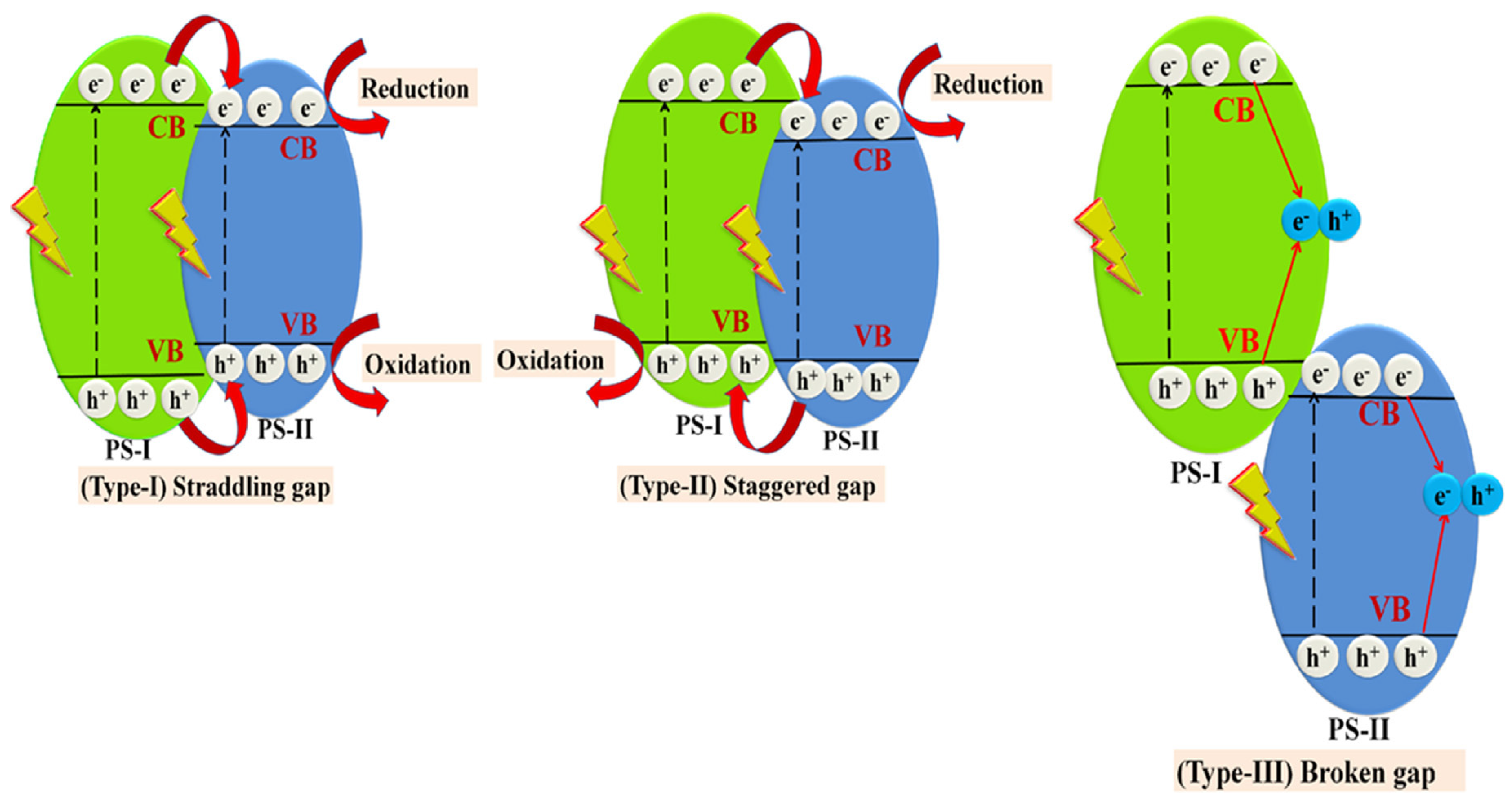
  • Type-I (straddling gap)—CB energy in the semiconductor “I” is higher, while VB potential is lower than in the semiconductor “II”, so that both electrons and holes can migrate towards the semiconductor “II”.
  • Type-II (staggered gap)—CB and VB energies of the semiconductor “I” are lower than in case of the semiconductor “II”, so electrons can migrate towards the semiconductor “II”, while holes move in the opposite direction, leading to spatial electron-hole separation.
  • Type-III (broken gap)—VB energy in the semiconductor “I” is lower than the CB energy in the semiconductor “II”, resulting in no transfer or separation of electron–hole pairs.
Copper oxide/titanium oxide is one of the widest studied photocatalytic composites in various application. TiO2/Cu2O represents a type-II heterojunction, while TiO2/CuO shows a type-I interaction. Copper oxide/titanium oxide composites are typical examples of p-n junction heterostructures. The CuO-TiO2 was reported as a photocatalyst of organic compounds degradation [168,169,170], photoelectrocatalyst of water splitting [171,172] and carbon dioxide reduction [173]. Copper and titanium oxides have multiple roles in composite. The most important advantage results from the formation of p-n junction. The n-type material (TiO2) has a high electron concentration, while the p-type (CuO) a high hole concentration, thus electrons diffuse towards the p-type region and holes towards the n-type one, leaving behind exposed charges (positive or negative) on dopant atom sites. An electric field between the positive and negative ion cores is called a depletion region and the presence of this effect is facilitating the charge separation between electrons and holes [171]. Furthermore, the presence of copper oxide in titanium material extends the range of light absorption [170], acts as a cocatalyst [169] and can affect the reaction mechanism [173]. General mechanism of photoactivity of the CuO-TiO2 composite is based on the transfer of photoinduced electrons from the conduction band of TiO2 to the conduction band of CuO. A different mechanism occurs in the case of Cu2O-TiO2. Since the CB potential of Cu2O is more negative than the one of TiO2, under irradiation electrons from CB of Cu2O are transferred towards TiO2 [174]. Similar to the case of CuO-TiO2, Cu2O-TiO2 exhibits an improved activity of photo(electro)catalytic reaction in comparison with bare oxides. Recent literature examples include: Cu2O/TiO2 nanotubes or Cu2O/TiO2 octahedron for H2 evolution under sunlight [175,176], Cu2O/TiO2 or Cu–Cu2O/TiO2 heterojunction photocatalysts for dyes degradation [177,178].
The CuO/Fe3O4 type-II heterojunction was studied towards the photocatalytic degradation of organics [179]. An enhanced photocatalytic activity of the heterojunction in comparison with bare CuO and Fe2O3 was assigned to the improved separation between charge carriers, a declined band gap energy, a large surface area, and the suppressed recombination of charge carriers. The studied heterojunction showed extended durability upon working conditions up to five times.
Copper-zinc oxide nanoflowers prepared by hydrothermal route showed the hydrogen evolution in pure water, while in the presence of sacrificial hole scavenger (triethanolamine) the yield of reaction increased four times [180]. Further examples of photo(electro)catalyst type-II heterojunctions are: WO3/Cu2O [181], In2O3/CuO [182,183], NiO/Cu2O [184], CeO2/CuO [185], CdS/Cu2O [186], ZnS/Cu2O [187] and CuS/CuO [188].
Z-scheme is a kind of heterojunction construction proposed to optimize the drawbacks of lower redox potentials of heterojunction system. Specifically, there are two types of Z-scheme composites—direct and indirect (Figure 15). Indirect systems required the presence of an electron mediator to provide an efficient electron transfer between the two semiconductors. Recent literature shows a few examples of Z-scheme composites based on copper oxides. The CuO-Bi-BiOBr system was studied for enhanced sunlight driven alcohol oxidation [189]. In this case, bismuth particles act as an electron mediator and connector between the BiOBr and CuO. Titanium dioxide and copper(I) oxide, with silver nanoparticles as a mediator, form the Z-scheme photocatalyst of water splitting with hydrogen evolution [190]. This system can effectively work also without electron mediator. Titanium dioxide and copper oxide can be connected also using other, more complex compounds (e.g., Ti3C2Tx [191]). Double-shelled hollow Z-scheme system Cu2O@CuCo2O4 was reported as a photocatalyst for organics degradation [192]. In an interesting approach, a copper-based Z-scheme uses a copper electron mediator to connect copper oxide with other semiconductors. This approach is represented by Cu2O/Cu/AgBr/Ag or Cu2O/Cu/g-C3N4, which were tested towards pollutants degradation [193,194]. The latter system is an example of carbon/copper composites, discussed below in detail.

2.6. Carbon Based Composites

Because of the narrow band gap, copper oxide nanoparticles are characterized by a relatively high probability of electron-holes pair recombination, which leads to significantly decreased photoactivity. To compensate this drawback, various carbonaceous materials such as carbon nanotubes (CNT), graphene, graphene oxide (GO) or graphitic carbon nitride (g-C3N4) have gained attention. Carbonaceous materials act in a several ways: They decrease the rate of unfavorable recombination thanks to a mutual charge transition, offer support for anchoring metal oxides and increase the specific surface area. Moreover, generated charge carriers in copper oxides grains cannot be efficiently transferred to the surface due to poor conductivity, so it is meaningful to combine copper oxides with high conductivity materials such as carbon nanotubes [196]. Another advantage of carbonaceous materials is their high chemical stability.
A CuO/CNT composite was prepared by electrolysis and has been tested for the photocatalytic degradation of p-chloroaniline [197]. TEM analyses clearly indicate the tube-shaped materials (CNT) organized in bigger linear structures and the CuO nanoparticles with the crystallite size less than 20 nm. From the FTIR results, bands corresponding Cu–O–C bonds confirmed the interaction between CuO and CNT. Finally, it has been demonstrated that the photoefficiency of p-chloroaniline degradation increases with increasing load of CNT, up to 50 wt%. Other carbonaceous materials like the CNTs/Cu2O-CuO photocatalyst was synthetized by a spray pyrolysis method, using copper acetate and CNT dispersion as a substrates [196]. Experimental research demonstrated the numerous effects related to the formation of composite with CNT, such as 30% higher specific surface area and a doubled reaction yield towards degradation of organic dye.
Graphene, graphene oxide and reduced graphene oxide attracted large interest as a support for many photocatalyst, including CuO and Cu2O. Such materials have been summarized in numerous review articles [173,198,199]. First of all, combination of copper oxide materials with a highly conductive graphene framework is an attractive approach to assemble efficient photocathodes for solar fuel generation. Kecsenovity et al. described the multiple potential-step electrochemical deposition of copper(I) oxide on the surface of graphene and graphene foams [200]. The PEC activity towards CO2 reduction was deeply studied: Graphene-containing photocathodes showed improved properties in comparison with pure Cu2O, both in terms of the achieved current densities and stability. Electrochemical analyses demonstrated that the main contribution of the graphene component was the facilitation of charge separation and transport, leading to an improved harvesting of the generated charge carriers. The proposed mechanism of activity includes: (1) Photoinduced electron transition from Cu2O to CO2; (2) recombination of electrons and holes in the space charge area; (3) hole transfer from copper oxide to graphene, and (4) hole transport to the current collector. Furthermore, graphene-type materials/semiconductor composites were demonstrated also to possess improved optical properties: A notable lowering of band gap energy of Cu2O/GO composite with an increasing graphene oxide amount has been observed which is due to the formation of sub-bands between the valence and conduction bands of Cu2O, as confirmed by Urbach energy analysis [201].
Among all graphene materials, reduced graphene oxide (rGO) has been attracting the highest attention. rGO is a form of graphene oxide treated by chemical, thermal, photochemical and other methods in order to reduce the oxygen content. Graphene has a serious agglomeration because of the strong interaction between the layers. In turn, graphene oxide has a lowered electrical conductivity due to the oxygen-containing functional groups on the surface. Therefore, thanks to the elimination of oxygen groups, rGO seems to be free of these negative effects. The presence of Cu2O nanograins on rGO sheets can successfully ameliorate the agglomeration issue between layers while, thanks to the improved electrical conductivity, photogenerated electrons from the CB of copper oxide can be transferred instantly via rGO sheets leading to a decrease of the unfavorable recombination of carriers [202]. Such promising effects resulted in numerous example of photocatalytic and photoelectrochemical application of copper oxide/rGO: Cu2O/rGO and CuO/rGO as visible-light active catalysts of CO2 photoreduction to methanol [203,204], Cu2O/rGO towards photocatalytic degradation of pollutants [205,206,207] and Cu2O/RGO and CuO/RGO nanocomposites for photocatalytic and photoelectrochemical H2 evolution [198,199,208].
More complex, multicomponent materials based on copper oxide and graphene oxide were also investigated, for example, Jang et al. reported delafossite CuFeO2/NiFe/reduced graphene oxide photoelectrocatalyst with high photoactivity of −2.4 mA cm−2 at 0.4 V RHE in NaOH electrolyte [149]. The Cu2O/reduced graphene oxide/TiO2 (Cu2O/rGO/TiO2) photocatalyst synthesized under ultrasonic irradiation was studied in “click” reaction for the synthesis of 1,2,3-triazoles via one pot multicomponent reaction of benzyl halide or epoxide derivatives with alkynes under visible light irradiation [209].
Finally, composites of copper oxide with g-C3N4 were recently reported by Wojtyła et al. [205,210]. CuO/g-C3N4 photocatalysts have been successfully synthesized by exfoliation of a bulk graphitic carbon nitride and subsequent hydrothermal decoration with CuO nanoparticles. Such methodology resulted in composites with a low amount (up to 5%) of copper oxide at monolayer g-C3N4. The addition of CuO significantly enhanced the light adsorption in the visible-light region (Figure 16A) and reduces (towards more negative values) the flat band potential. Composites were able to generate high density cathodic photocurrent (Figure 16B), while irradiating the material suspension leads to water splitting with hydrogen evolution even without a sacrificial electron donor (Figure 16C). The improved photocatalytic and photoelectrochemical activity of CuO/g-C3N4 results from the formation of type-II heterostructure and mutual charge transition [205]. In such heterostructures, the differences of chemical potential between semiconductors result in band bending at the interface of junction, which drives the electrons and holes to move in opposite directions, resulting in a spatial separation of the photogenerated charge carriers on different sides of heterojunction.
In contrast, Mitra et al. and Liu et al. investigated copper(I) oxide/graphitic carbon nitride composites [211,212]. The theoretical calculations demonstrated that the sp2 hybridized nitrogen atoms of g-C3N4 may act as binding sites to connect the Cu2O. Spectroscopic studies confirmed the lowering of band gap energy of materials with increasing of Cu content. These nanomaterials were investigated as photocatalysts for organics degradation. Interestingly, it was observed by XPS analysis that the oxidation state of Cu varies with its concentration in the composites [211]. Graphitic carbon nitride and copper oxide can form a Z-scheme system photocatalyst [194].

2.7. Surface Modified/Functionalized Copper Oxides

Surface modification of a semiconductor can be performed using organic or inorganic chromophores. Different mechanisms of interaction can be distinguished [206,207]:
  • Direct photosensitization (optical charge transfer), observed in the presence of surface metal to metal charge transfer (MMCT) or ligand to metal charge transfer (LMCT);
  • An electron injection from the excited photosensitizer to the semiconductor’s CB.
  • A hole injection from the excited photosensitizer to the semiconductor’s VB.
The first mechanism involves a direct optical electron injection (OET—optical electron transfer) through the excitation of a photosensitizer-semiconductor complex created upon chemisorption of organic or inorganic ligands onto semiconductor. A LMCT or MMCT are at the basis of the electron injection to the conduction band. The other two mechanisms involve the excitation of the surface bound chromophores followed by an interfacial electron transfer from the excited state of the modifier to the CB of the semiconductor (photoinduced electron transfer) or a hole injection from the excited state of the modifier to the valence band of the semiconductor (photoinduced hole transfer). In both cases, the semiconductor can be in the fundamental or in excited states. Good modifiers should have a strong light absorption, have long lifetimes of the excited states, exist in stable oxidized and reduced forms and do not have the tendency to aggregate or degrade. Regardless of the mechanism, surface modifiers can play various roles (e.g., enlarge the light absorption range, act as an electron mediator or cocatalyst and improve the adsorption of reagents).
The Grätzel group reported Cu2O photocathode modified with a rhenium bipyridyl catalyst [213]. Such a system was used towards photoelectrochemical reduction of CO2 to CO. It has been found that, upon irradiation, electrons from the CB of Cu2O can be transferred through the CB of TiO2 (protective layer) to the rhenium complex (Re(tBu-bipy)(CO)3Cl), which is a real catalyst of carbon dioxide reduction.
Dye-sensitized copper oxide is the next type of surface modification. Marathey et al. reported mercurochrome-sensitized CuO obtained directly on Cu, which was studied as photocathode in photoelectrochemical cell [214]. Mercurochrome (called also merbromin) is a xanthene dye, an organometallic compound containing mercury atom. Modified nanomaterial exhibits better PEC efficiency (more than two times higher photocurrent density) through an effect of carrier injection from the excited dye to the excited semiconductor (Figure 17). The main advantages of the proposed system are a strong light harvesting ability of the dye and fast electron injection kinetics.
Increased photocurrents were observed also in the case of dye-modified Cu2O. A series of dyes have been investigated as electron donors (ZnP-A, C343, N3) or acceptors (C60M-A, NcQ-A, PTCDA) [215]. Experimental results demonstrate that the Cu2O/dye/electrolyte interface shows significant differences in the balance of forward/back electron transport in comparison with the pure Cu2O/electrolyte interface. In principle, each dye in its basic state should be able of accepting a photogenerated electrons from the conduction band of Cu2O (based on redox properties). However, various dyes showed different mechanisms for increasing photocurrents.
Recently, semiconductors modified with MOF (metal-organic framework) structures gained attention. Cu3(btc)2 (where btc—1,3,5-benzene tricarboxylate)-decorated cuprous oxide nanowires can be given as an example of such system investigated in photoreduction of CO2 [216]. The MOF compound leads to the suppression of the corrosion of Cu2O and also facilitate charge separation and improves CO2 adsorption. Experimental photoluminescence results proved the direct transfer of photogenerated electrons from the CB of Cu2O to the LUMO level of non-excited Cu3(BTC)2. Similar mechanism of improved photoactivity was observed also in case of a more complex system: TiO2/Cu2O/ Cu3(btc)2 [217].

3. Further Approaches of Photo-Efficiency Improving

3.1. Underlayers and Overlayers for Efficient Charge Transport

Cu2O is an outstanding p-type photocathode for PEC water splitting since it has a direct band gap of 2 eV and a corresponding theoretical photocurrent of −14.7 mAcm−2, and a light-to-hydrogen conversion efficiency of 18% based on the AM1.5 spectrum [218]. However, the redox potential for reduction and oxidation of monovalent copper oxide is within its band gap and the reactions are like Equations (5) and (6), which lead to poor stability and limits its application.
Cu 2 O + H 2 O + 2 e   2 Cu + 2 OH ( + 0.47   V   vs .   SHE ,   pH = 0 )
2 CuO + H 2 O + 2 e -   Cu 2 O + 2 OH ( + 0.6   V   vs .   SHE ,   pH = 0 )
To inhibit this process, the deposition of a suitable overlayer is the most common strategy to block these reactions, by inhibiting photo-generated electron transfers to the surface of Cu2O (and CuO) through insulating the latter from the electrolyte. As a protective layer to passivate the surface of Cu2O, the design should follow some guidelines: (1) The layer should have small resistance and the photo-generated electrons and holes can transfer from the Cu2O to the solution; (2) this corresponds to a staggered type-II, and then the photogenerated electrons can flow from the Cu2O through the protective layer to the electrolyte to promote water reduction, whereas holes flow into the Cu2O bulk [48]; (3) the layer should be chemically stable in the reaction conditions. According to these principles, the protective overlayer/underlayer usually forms a n-p heterojunction to allow the transfer of photo-generated holes.
After illumination, electron-hole pairs are generated, and the photo-generated electrons will transfer from the conduction band of the p-type Cu2O to the n-type semiconductor, where they accumulate in the conduction band. This extends the lifetime of electrons, thus inhibiting charge recombination. Besides, photogenerated holes will transfer from the n-type semiconductor to Cu2O. As a result, this mechanism overcomes charge recombination, and then the photo-generated electrons have more chance to be involved in the desired reduction process. Quite importantly, the valence band of p-type Cu2O is just slightly lower than the potential of oxygen evolution. However, after being in contact, the valence band of the n-type semiconductor can better meet the potential for oxygen evolution reaction (OER) [219]. Thence, the p-n heterojunction can enhance the performance and block the self-oxidation of Cu2O as a protective layer. Many n-type semiconductors, Ga2O3 [220,221,222,223], ZnO [224,225], TiO2 [226,227] and NiOx [50], deposited over Cu2O can enhance the performance, since the n-type semiconductor and p-type semiconductor can provide holes and electrons for the water splitting, respectively, as well as relative band positions. Several Cu2O-based n-p heterojunctions behave as schematized in Figure 18. After the contact, a built-in electric field is set, which can lead the photo-generated electrons transport thus prolonging the electrons lifetime and improving charge separation. In addition, this combination will enhance the light adsorption edge. Paracchino et al. adopted atomic layer deposition (ALD) to deposit TiO2 as a protective layer on Cu2O and forming a highly active photocathode for solar H2 production, which can protect against photocathodic decomposition. As a result, 5 *(4 nm ZnO/0.17 nm Al2O3)/11 nm TiO2 (it stands for five bilayers of 4 nm ZnO and 0.17 nm Al2O3, followed by 11 nm TiO2) showed best photocurrents of up to −7.6 mA cm−2 at a potential of 0 V vs RHE, and it can also remain active after 1 h test under AM 1.5 illumination at neutral pH. Meanwhile, the Faradaic efficiency was close to 100% [48]. Zhang et al. use a covalent triazine frameworks (CTF-BTh) containing a bithiophene moiety as a protective layer to deposit onto the surfaces of a Cu2O photocathode. At the same time, they constructed a Mo-doped BiVO4 photoanode via electropolymerization. CTF-BTh possesses a suitable band structure for a p–n junction and a staggered type-II heterojunction with Cu2O and Mo-doped BiVO4, respectively, which is a benefit to the water splitting process. Lastly, the CTF-BTh film plays an important role as an effective corrosion-resistant overlayer for both photoelectrodes to inhibit photocorrosion, and it lasts for long-term operation for 150 h with only ≈10% loss in photocurrent densities. Surprisingly, a standalone unbiased PEC tandem device comprising CTF-BTh-coated photoelectrodes exhibits 3.70% solar-to-hydrogen conversion efficiency and keeps continuous operation for 120 h, the efficiency can still retain at 3.24% [228].
A second strategy to protect the semiconductor is to deposit a hole transfer layer as an underlayer (i.e., between the conductive glass support and Cu2O). In this way, holes will transfer from Cu2O to the hole transfer layer to inhibit the recombination of photo-generated electron and hole pairs, thus overcoming the self-oxidation of Cu2O and enhance the performance of PEC water splitting. Pan et al. designed a Cu2O-based photocathode, using Ga2O3 and Cu2O forming a n-p heterojunction, as well as two different structures with CuSCN as the hole transport layers buried with TiO2 as a protective layer. Since the conduction band edge of CuSCN is at a higher potential than that of Cu2O, with a 2 eV band gap difference, a huge barrier for electrons transfer from Cu2O to CuSCN (towards the counter electrode) is generated. Enlarged XPS valence band spectra illustrated that an acceptor-like state near the Fermi level is generated and this can enhance the hole conductivity. Although CuSCN and Cu2O have very close valence band edges, the existence of band-tail states leads to a smooth hole transport, thus decreasing the probability of electron-hole recombination. As a result, this combination provides a solar-to-hydrogen efficiency of 4.55%, which is the highest efficiency among Cu2O based photocathodes [221]. Besides, other semiconductors can also be used as hole transfer layer, such as FeOOH [230] and NiO [231]. Zhou at al. firstly explored mechanism behind the stability of Cu2O and demonstrated that the accumulation of photogenerated holes in the valence band of Cu2O is a key factor. In this work, FeOOH was adopted as a hole transfer layer (HTL) and Pt was added as a cocatalytic layer (see below). As a result, photo-generated holes are transferred from the VB of Cu2O to FeOOH and then to a Pt counter-electrode through the external circuit. At the same time, photogenerated electrons are transferred from the conduction band of Cu2O to the Pt cocatalytic layer. The synergistic effect of the Pt layer and of FeOOH inhibits the recombination of photogenerated electrons and holes, which not only retard the self-oxidation of Cu2O, but also promotes the photoelectrocatalytic activity of Cu2O [230].
In addition, metals can be used as underlayers to improve Cu2O performances, and the most adopted ones are certainly Au [221] and Cu [53]. Cu2O-based photocathodes still employ Au as back contact due to the matching between gold work function and Cu2O valence band energy level. Low-cost Cu can replace Au, Cu/Cu2O showing similar performances to Au/Cu2O [53].
In summary, constructing a protective layer to overcome the photocorrosion of Cu2O and improve its performance mainly depends on enlarging the light adsorption edge, improving the separation efficiency of electron-hole pairs, changing the electron transfer path as well as prolonging the electrons’ lifetime.

3.2. Deposited Cocatalyst (Pt, Ag)

A transition metals, in particular noble metals are loaded on the semiconductors as a cocatalyst to enhance the photoefficiency of reaction. Cocatalysts deposited on surface of semiconductor can provide reaction active sites, catalyze the surface reactions by lowering the activation energy, trap the charge carriers (electron sink role) and suppress the unfavorable recombination of charges [232].
Cocatalyst may offer an alternative reaction mechanism characterized by a lower activation energy in comparison with the non-cocatalyzed pathway. For example, the theoretical minimum Gibbs free energy required for a water-splitting reaction is 237 kJ/mol. In practice, significantly higher energy is necessary to overcome the kinetic barriers for both HER and OER on photocatalyst. Proper cocatalysts can successfully reduce such energy barriers by lowering the activation energy (Figure 19). Particularly, water reduction usually requires much lower overpotential than water oxidation, so the role of cocatalyst in OER processes is more crucial. A direct correlation between the PEC yield and properties of the cocatalysts has been reported [233]. Among noble metals, platinum with higher redox potential and work function was identified to be the most favorable for HER. Instead, a volcano relationship between the exchange current for HER and the metal-hydrogen bond energy was proposed by Trasatti, and platinum showed the lowest activation energy for HER [234]. Therefore, Pt is considered as the most suitable cocatalyst for PEC H2 evolution from the viewpoint of electronic and catalytic properties.
In regard to improved charge separation effects when a cocatalyst is loaded on the semiconductor, a depletion layer at the cocatalyst/semiconductor interface is formed. A built-in electric field caused by the depletion layer can result in a driving force for efficient separation of the electron-hole pairs. That is to say, a suited cocatalyst enhances the efficiency of photogenerated charge separation and leads to a lowered rate of unfavorable recombination, a major reason for low photocatalytic activity.
Cocatalysts can be deposited on the surface of semiconducting materials using various methods: electrodeposition, photodeposition, wet impregnation, chemical reduction (e.g., impregnation-reduction method), atomic layer deposition, chemical vapor deposition, sputtering, glancing angle deposition, lithography and others. It has been proved, that the method of cocatalyst deposition may affect its role and effectiveness [235].
Recent literature offers numerous examples of cocatalyst deposited on copper oxide materials, both Cu2O and CuO. The cocatalysts can be classified into two roles: the cocatalyst trapping electrons for reduction half reactions (e.g., reduction of H2O or CO2) and the cocatalyst trapping holes for oxidation half reactions (e.g., oxidation of H2O or organic species). In general, noble metals (e.g., Pt, Pd, Rh and Au, Ru) [39,48,236,237,238,239,240], non-noble transition metals (e.g., Cu, Zn, Al, Co and Ni) [184,241,242,243,244,245], metal oxides (RuO2, NiOx, Bi2O3) [80,190,246,247,248] and metal sulfides (e.g., ZnS, MoS2, NiS, Ag2S, and WS2) [187,245,249,250,251] were reported as cocatalysts deposited on CuO and/or Cu2O.
Deposition of Pt or other cocatalysts on the surface of copper oxides resulted in a few effects. The most basic effects can be observed using photocurrents analysis. Copper oxide with deposited platinum showed significantly higher, even twice higher photocurrents densities [7,25]. Moreover, the photocurrent onset is shifted towards more positive potentials [240]. Xing et al. studied the influence of platinum on the photocorrosion of copper oxide [252]. They proved that Pt hinders the self-reduction of copper(II) oxide because of its fast electrons trap ability. Impedance studies on CuO/Pt photocathodes indicate that the photoinduced electrons transfer from the semiconductor to the electrolyte occurs more easily due to the presence of platinum, thereby suppressing the photocorrosion of CuO.

3.3. Surface Plasmon Enhancement Effects

In parallel to cocatalytic effect, the surface plasmon resonance can offer a new opportunity to overcome the low efficiency of photocatalytic reactions [253,254]. Light excitation of a metallic nanostructures leads to a strong optical near-field that induces a cascade of processes with multiple outcomes, including the excitation of surface plasmons, their radiative decay to photons, and their nonradiative decay in the material. The presence of plasmonic metal nanostructures on the surface of semiconductor photocatalysts can improve the photocatalytic efficiency due to: (i) Extending light absorption to visible light due to local dielectric environment alterations, (ii) increasing light scattering (metallic particles scatter incident light and locally amplify the electromagnetic field when placed on the surface of semiconductor), and (iii) exciting electron−hole pairs in the semiconductor by transferring the plasmonic energy from the metal to the semiconductor with various proposed models of energy transfer, as shown in Figure 20. Direct electron transfer (DET) from the metal to the semiconductor’s CB may occur only if they are in direct contact and DET depends on the mutual alignment of the CB and Fermi level of the metal. Another suggested mechanism of energy transfer from plasmonic metal is called surface plasmon resonance mediated local electromagnetic field LEMF and can lead to charges generation in the semiconductor. The charge separation induced by LEMF may form carriers only for energies above the band gap of the semiconducting material. LEMF increases the rate of interband transitions in the semiconductor because of the rise of local electromagnetic field. Moreover, resonant energy transfer (RET) was suggested in the literature as an alternative, nonradiative mechanism of surface plasmon resonance induced charge separation in semiconductors, in contrast to the radiative LEMF model [253]. This process directly induces the electron and hole in the semiconductor nonradiatively by the relaxation of the localized surface plasmon dipole. Described proposed mechanism are not clear and they require additional study in order to find their influence on photocatalytic reaction efficiency.
Surface plasmon effects are typically observed for metals such as gold or silver. The CuO-Au nanohybrids showed enhanced visible light absorption properties, four times higher photocurrents and significantly improved kinetic of reaction [246]. The enhanced photocatalytic activity was attributed to the surface plasmon resonance effect of Au NPs. Similar, thin films, composed of bimetallic Au-Ag nanoparticles deposited on a CuO showed Localized Surface Plasmon Resonance (LSPR) responsible for significantly improved light absorption [255]. Hajimammadov and co-workers proved surface plasmon effects in case of copper metallic nanoparticles on Cu2O/CuO composite [256].

4. Application of Copper Oxide-Based Materials in Photocatalysis and Photoelectrocatalysis

4.1. H2 Evolution

In the future of hydrogen economy, photoelectrochemical water splitting is one of the most promising alternatives for renewable hydrogen generation and storage. The process simply needs water, sun and a semiconducting material. Obviously, the photocathode and photoanode must have the appropriate band gap and bands alignment with respect to the HER and the OER, respectively. In the working configuration, the semiconductor was immersed in a water-based electrolyte, with sunlight being the driving force for charges generation inside valence and conduction bands. These charges are the energy source for the water splitting reaction.
Under light, photons possessing more energy than Eg are absorbed by the material and electrons are excited from the VB to the CB, generating electrons-holes couples. An applied electric field can force the separation between photogenerated electrons and holes. In doped semiconductors, band banding is generated after the immersion in the electrolyte and induced a potential gradient within the material. In a p-type material, this attracts electrons towards the solution, while holes move toward the bulk semiconductor and then to the counter electrode. The use of an external bias can be useful to overcome eventual overpotentials, to improves the band bending giving an efficient charges separation or to compensate for the insufficient position of band edges with respect to the semi-reactions of interest [257,258]. There are some requirements for a PEC-WS system to work properly:
  • An efficient absorption of solar light to produce excited states in the semiconductor.
  • A good charge separation to avoid recombination of the electron-hole couple and ensure a high light-to-chemicals conversion.
  • Proper bands position with respect to HER and OER from thermodynamic and kinetic points of view.
  • High stability to photodegradation processes.
Accomplishing all of these needs is not simple. Many semiconductors able to perform the desired reaction without undergoing photodegradation show a wide band gap that reduces the portion of solar spectra available for the absorption (e.g., TiO2 with a 3 eV band gap can absorb only in the UV) [7]. Despite this, compared to other H2 production routes, PEC-WS has the advantage of having a relatively simple and cheap process. It does not require expensive setups, is completely based on renewable sources and has no by-products. It can also work in wide range of temperatures and without a warm-up step (if the temperature is above 0 °C). Once all the requirements are satisfied at the photoanode, reaction (1) takes place.
While at the photocathode, water reduction will occur using the high-energy electrons excited in the CB by the solar light (Equation (2)).
The so produced hydrogen can be collected and stored to be used when required for examples in fuel cells or as a chemical in the oil industry.
The desired electrons transfer is not the only available route for holes and electrons. Figure 21 summarizes the possible processes following the photon absorption in a semiconductor immersed in an electrolyte with a donor D and an acceptor A. Once the light-excited electrons and holes are moved at the corresponding edges of energy bands they may undergo trapping (reactive and non-reactive) on surface sites as well as radiative and nonradiative recombination. These alternative routes for the electron-hole couple will reduce the conversion efficiency of sunlight to chemical products.
In materials like Cu2O, but also ZnS or CdS, the main path for the material photodegradation (photocorrosion) is the electron-transfer reaction to the material itself (reaction not included in the scheme). This happens when the redox potential of the material lies within the band gap. As a result, electrons (but also holes) react with the semiconductor itself leading to a reduction to the corresponding metals. This photo-degradation reaction is even stronger for very pure materials suggesting the importance of doping [259].
The main PEC-WS challenges that have to be overcome in this system are:
  • Extended lifetime for photoelectrode materials and thus limited (photo)corrosion processes.
  • The right bands edge alignment for the redox reactions from a thermodynamic point of view.
  • Fast kinetics for HER/OER.
  • A suitable optical band gap for optimal light absorption and high photon efficiencies.
  • A fast charges transport in the bulk semiconductor.
  • Low internal electrical resistance.
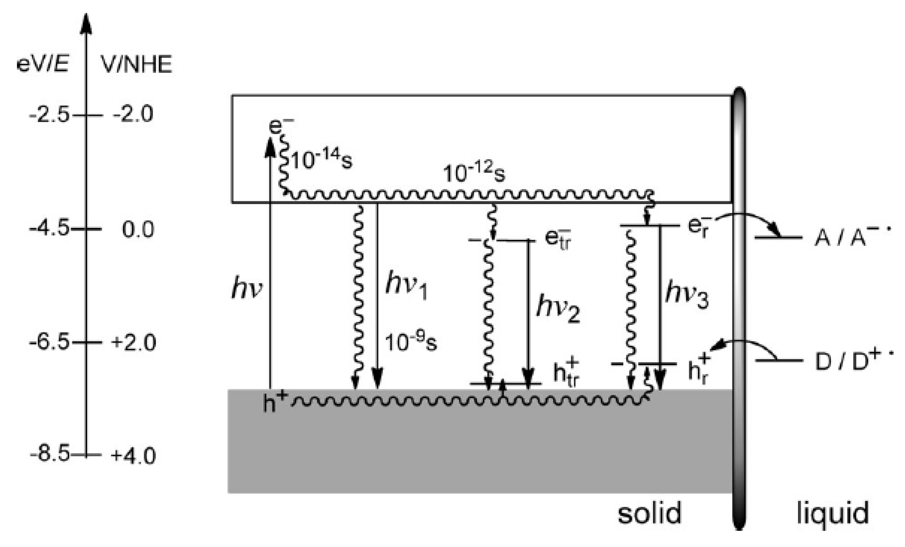
  • Limited phenomenon like trapping and recombination (see Figure 21).
  • Low-cost materials with wide availability and reduced plant capital costs.
The semiconductor-based PEC-WS is nowadays an almost mature technology to be a valid solution for near-future energy storage. Despite the high cost for the H2 production in PEC-WS systems, the continuous improvements in the field are promising for the future scalability of this technology.

4.2. CO2 Reduction to Methane and Other C1 Compounds

The use of sunlight to convert carbon dioxide into fuels, such as methanol, methane or formic acid, might contribute to solving two global problems: high emission of CO2 into the atmosphere and depletion of fossil fuels [247]. In heterogeneous photocatalytic reduction of CO2, the reaction takes place at a solid-gas or solid-liquid interface, and the photocatalysts are often hybrid materials realizing several tasks: (i) Light absorption, (ii) separation of the photogenerated charges, (iii) transfer of charges to the surface and (iv) redox reactions at active sites. The adsorption of carbon dioxide on a photocatalyst surface is the first step of photocatalytic activation of CO2, that leads to the formation of a partially charged species (CO2δ•-) and loss of the linear symmetry of the molecule. Consequently, the barrier for accepting an electron in further photocatalytic process is lowered [248]. The electron transfer from the excited semiconductor to the CO2 molecule adsorbed at the material’s surface initiates the cascade of processes involving the cleavage of C-O bonds and formation of C-H bonds. One electron reduction of CO2 to its anion radical is a thermodynamically unfavorable reaction, in part because the additional electron must occupy the lowest energy π* orbital of CO2 [260]. The addition of one electron causes bending of the molecule from 180° to about 120°. The loss of symmetry is related with a repulsion between free electron pair at the oxygen atoms and one extra electron localized at the carbon atom. Direct one-electron reduction of CO2 leads to the formation of the carbon dioxide radical anion CO2¯. The redox potential of the CO2/CO2¯ couple in water amounts to −1.9 V vs. a standard hydrogen electrode and, therefore, only semiconductors characterized by particularly negative potential of conduction band can be used as a photocatalyst of one-electron reduction of CO2 (e.g., ZnS or SiC) [260,261,262].
In contrast, a proton-assisted multielectron reduction of carbon dioxide leads to a variety of stable products making such reactions thermodynamically preferred. The number of transferred electrons (up to eight) determines the final oxidation state of the carbon atom [263]:
CO2 + 2H+ + 2e→ HCOOH E° = −0.250 V
CO2 + 2H+ + 2e → CO + H2O E° = −0.106 V
CO2 + 4H+ + 4e→ HCHO + H2O E° = −0.07 V
CO2 + 6H+ + 6e → CH3OH + H2O E° = 0.016 V
CO2 + 8H+ + 8e → CH4 + 2H2O E° = 0.169 V
The redox potentials of CO2 reduction to CO, HCOOH, HCHO, CH3OH or CH4 are noticeably higher (less negative) than the conduction band edge potential of many common semiconductors (e.g., CuO, Cu2O or TiO2), thus photocatalysis can be successfully applied to these processes. These strategies of carbon dioxide reduction can be performed also in a photoelectrochemical way, as discussed in more detail elsewhere [264].

4.3. Degradation of Organic Species in Liquid or Gas Phase

Photocatalytic degradation of organic species such as VOC (volatile organic compounds), dyes, pesticides or pharmaceuticals is an approach of environment remediation using a broad variety of photoactive materials. Technology readiness levels of these processes are very high, and many semiconducting materials demonstrated acceptable photocatalytic efficiency in a real space environment. Removal of indoor VOC pollutants has been already implemented in the economy, since photocatalytic air purifier or purification systems are commercially available. Process of organic compounds degradation includes a few stages: (i) Mass transfer of the organics to the surface of the photocatalyst, (ii) adsorption of the molecules onto the active sites, (iii) photocatalytic degradation, (iv) desorption of the products of degradation and (v) mass transfer of these products away from the photocatalyst’s surface [265].
The mechanism of photocatalytic degradation of organic species is not simple because it involves two main steps. Semiconductors absorb light to generate pairs of electrons and holes. These charges react with oxygen or water (steam) to form reactive oxygen species (ROS), such as hydroxyl radicals, superoxide anion radicals, singlet oxygen, hydrogen peroxide and others. The mechanism of ROS formation via photocatalysis is well know from the literature and has been shown in Figure 22 [266]. In a second step, ROS are the key oxidants that decompose organic pollutants via the so-called advanced oxidation processes. ROS possess higher reaction activity than O2 and can completely destroy a very broad range of organic pollutants including organic halides and polycyclic aromatic hydrocarbons. At the same time, some organics can be directly oxidized by photogenerated holes [267]. Photocatalytic oxidation of VOC and other organic compounds leads to safe products such as CO2, CO and H2O.
Despite many advantages, photocatalytic purification of air or wastewater has serious limitations, such as a slow rate and low quantum efficiency. More information on the photocatalytic degradation of VOC in gas phase or decomposition of dyes, pesticides or pharmaceuticals in liquid phase can be found in recent reviews [265,268,269,270].

4.4. Other Photocatalytic Processes

Copper-based materials can be used as a photocatalyst also in many other photocatalytic processes such as: removal of heavy metals from wastewater, photocatalytic abatement of NOx pollutants in the air or photo(electro)catalytic regeneration of cofactors such as NADH (nicotinamide adenine dinucleotide coenzyme).
Metal ions are generally not decomposed, but various photocatalytic strategies have been suggested to eliminate heavy metals from wastewater, in particular, reductive and oxidative strategies [271]. Heavy metals and metalloids removal from water basically involves reduction process that produce elemental metals (can be easier removed by other techniques) or metal ions at a lower oxidation state, that are less toxic (e.g., toxic chromium(VI) reduced to non-toxic chromium(III) [272]). The oxidative strategy can be considered in case of arsenic, which occurs in the anionic form and has to be oxidized to be removed [271].
Regenerated NAD cofactor (NADH) can be considered as a form of energy storage that can be used, for example, in enzymatic conversion of CO2 to methanol. Enzymatic reduction of carbon dioxide is catalyzed by some enzymes, such as formate dehydrogenase, formaldehyde dehydrogenase and alcohol dehydrogenase, while the necessary energy is provided by NADH [273]. In each enzymatic step, one mole of NADH is oxidized to NAD+ that must be converted back to NADH. This regeneration can be performed in a photoelectrochemical or photocatalytic way, in a simple system or with an electron mediators such as a ruthenium complex [273,274].

5. Conclusions

In this review we analyzed and discussed the use of Cu-based materials as photoactive materials in different reactions, including water splitting, CO2 reduction and the remediation of wastewaters. Cu is a relatively abundant element and its compounds can be easily prepared and manipulated. Playing on the oxidation state of Cu and the possibility of synthetizing ternary and quaternary oxides, as well as of tuning the electronic properties of these materials by doping, it is possible to prepare a semiconductor with the desired characteristics.
Finally, the performances of the final material can be further improved by addition of an overlayer or underlayer, of a cocatalyst or by a combination with a carbonaceous material. We are still far from a material that can sustain the needs of an industrial-level photochemical or photoelectrochemical device, but we here demonstrate that researchers have jumped big leaps in the last five to 10 years by proposing highly active and stable materials, and by better understanding the principle that we should follow for synthetizing the new generation ones.
We can conclude this review in saying that, thanks to these findings, it is now possible to optimize the design of a Cu-based photocathode by acting on the synthesis (with a preference for low-cost, easy scalable methods), doping and addition of under/overlayers and cocatalysts/plasmonic effect-inducing particles. This, in turn, will not be an easy task, mostly due to the increasing number of variables, such as the nature of the precursor, the semiconductor synthesis method and its parameters, the synthesis method and its parameters for the underlayer, the synthesis method and its parameters for the overlayer, the synthesis method and its parameters for the cocatalyst and, finally, the possible methods to build this complex architecture. We foresee that the adoption of combinatorial chemistry methods aimed at the rapid screening of material libraries’ activity [275,276,277] could represent a great help in this sense.

Funding

This research was funded by the Jane and Aatos Erkko Foundation, grant: “Renewable energy storage to high value chemicals”; the Italian Ministry of University, grant number Prot. 2017YH9MRK; the Università degli Studi di Milano, grant number PSR 2020.

Acknowledgments

M.B. acknowledges financial support from the Jane and Aatos Erkko Foundation through the “Renewable energy storage to high value chemicals” project. A.M., A.V. and S.R. acknowledge the financial support of MIUR: Prot. 2017YH9MRK; and of the Università degli Studi di Milano.

Conflicts of Interest

The authors declare no conflict of interest.

References

  1. Paola, A.; Nicolas, B.; Erika, C.; Richard, J.; Gerhard, K.; Jochem, M.; Vaishali, N.; Matthew, P.; Plattner, G.-K.; Joeri, R.; et al. Climate Change 2021: The Physical Science Basis. Contribution of Working Group14 I to the Sixth Assessment Report of the Intergovernmental Panel on Climate Change; Technical Summary; eLib, Posted 22 November 2021. Available online: https://elib.dlr.de/137584/ (accessed on 29 November 2021).
  2. Lewis, N.S.; Nocera, D.G. Powering the planet: Chemical challenges in solar energy utilization. Proc. Natl. Acad. Sci. USA 2006, 103, 15729–15735. [Google Scholar] [CrossRef] [PubMed] [Green Version]
  3. Rodriguez, C.A.; Modestino, M.A.; Psaltis, D.; Moser, C. Design and cost considerations for practical solar-hydrogen generators. Energy Environ. Sci. 2014, 7, 3828–3835. [Google Scholar] [CrossRef] [Green Version]
  4. Ager, J.W.; Shaner, M.R.; Walczak, K.A.; Sharp, I.D.; Ardo, S. Experimental demonstrations of spontaneous, solar-driven photoelectrochemical water splitting. Energy Environ. Sci. 2015, 8, 2811–2824. [Google Scholar] [CrossRef] [Green Version]
  5. Pinaud, B.A.; Benck, J.D.; Seitz, L.C.; Forman, A.J.; Chen, Z.; Deutsch, T.G.; James, B.D.; Baum, K.N.; Baum, G.N.; Ardo, S.; et al. Technical and economic feasibility of centralized facilities for solar hydrogen production via photocatalysis and photoelectrochemistry. Energy Environ. Sci. 2013, 6, 1983–2002. [Google Scholar] [CrossRef] [Green Version]
  6. Jiang, C.; Moniz, S.J.A.; Wang, A.; Zhang, T.; Tang, J. Photoelectrochemical devices for solar water splitting-materials and challenges. Chem. Soc. Rev. 2017, 46, 4645–4660. [Google Scholar] [CrossRef] [PubMed] [Green Version]
  7. Jiménez Reinosa, J.; Leret, P.; Álvarez-Docio, C.M.; Del Campo, A.; Fernández, J.F. Enhancement of UV absorption behavior in ZnO-TiO2 composites. Bol. Soc. Esp. Ceram. Vidrio 2016, 55, 55–62. [Google Scholar] [CrossRef] [Green Version]
  8. Tang, S.J.; Moniz, S.J.A.; Shevlin, S.A.; Martin, D.J.; Guo, Z.-X.; Tang, J. Visible-light driven heterojunction photocatalysts for water splitting—A critical review. Energy Environ. Sci. 2015, 8, 731–759. [Google Scholar] [CrossRef]
  9. Chen, S.; Wang, L.-W. Thermodynamic Oxidation and Reduction Potentials of Photocatalytic Semiconductors in Aqueous Solution. Chem. Mater. 2012, 24, 3659–3666. [Google Scholar] [CrossRef] [Green Version]
  10. Jiang, Y.; Yuan, H.; Chen, H. Enhanced visible light photocatalytic activity of Cu2O via cationic-anionic passivated codoping. Phys. Chem. Chem. Phys. 2014, 17, 630–637. [Google Scholar] [CrossRef]
  11. De Jongh, P.E.; Vanmaekelbergh, D.; Kelly, J.J. Cu2O: A catalyst for the photochemical decomposition of water? Chem. Commun. 1999, 1069–1070. [Google Scholar] [CrossRef]
  12. Siavash Moakhar, R.; Hosseini-Hosseinabad, S.M.; Masudy-Panah, S.; Seza, A.; Jalali, M.; Fallah-Arani, H.; Dabir, F.; Gholipour, S.; Abdi, Y.; Bagheri-Hariri, M.; et al. Photoelectrochemical Water-Splitting Using CuO-Based Electrodes for Hydrogen Production: A Review. Adv. Mater. 2021, 33. [Google Scholar] [CrossRef] [PubMed]
  13. Forsyth, J.B.; Hull, S. The effect of hydrostatic pressure on the ambient temperature structure of CuO. J. Phys. Condens. Matter 1991, 3, 5257–5261. [Google Scholar] [CrossRef]
  14. Koffyberg, F.P.; Benko, F.A. A photoelectrochemical determination of the position of the conduction and valence band edges of p-type CuO. J. Appl. Phys. 1982, 53, 1173–1177. [Google Scholar] [CrossRef]
  15. Rakhshani, A.E. Preparation, characteristics and photovoltaic properties of cuprous oxide—A review. Solid. State. Electron. 1986, 29, 7–17. [Google Scholar] [CrossRef]
  16. Chaudhary, Y.S.; Agrawal, A.; Shrivastav, R.; Satsangi, V.R.; Dass, S. A study on the photoelectrochemical properties of copper oxide thin films. Int. J. Hydrog. Energy 2004, 29, 131–134. [Google Scholar] [CrossRef]
  17. Aktar, A.; Ahmmed, S.; Hossain, J.; Ismail, A.B.M. Solution-Processed Synthesis of Copper Oxide (CuxO) Thin Films for Efficient Photocatalytic Solar Water Splitting. ACS Omega 2020, 5, 25125–25134. [Google Scholar] [CrossRef]
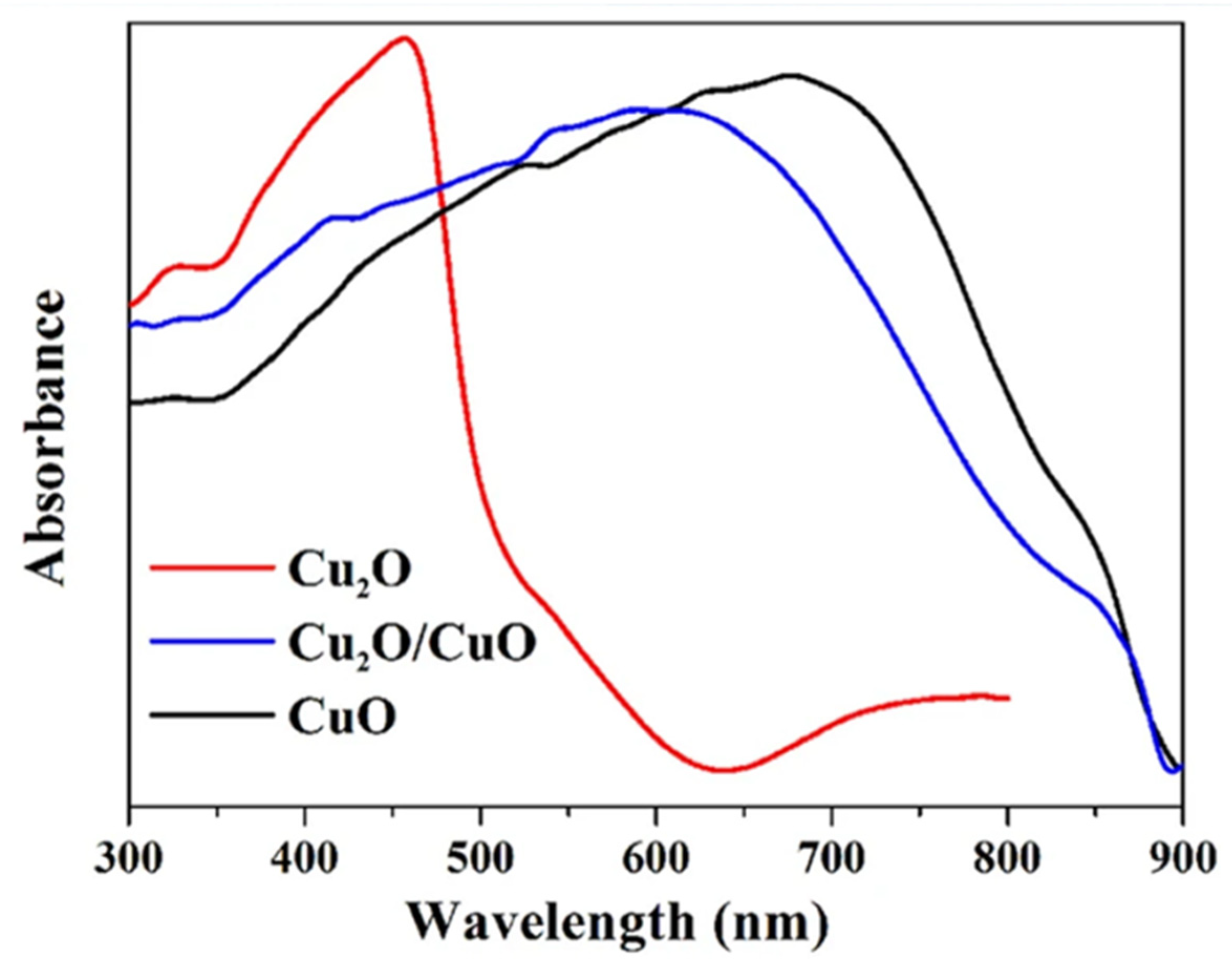
  18. Yang, Y.; Xu, D.; Wu, Q.; Diao, P. Cu2O/CuO bilayered composite as a high-efficiency photocathode for photoelectrochemical hydrogen evolution reaction. Sci. Rep. 2016, 6, 1–13. [Google Scholar] [CrossRef] [Green Version]
  19. Jun Seo, Y.; Arunachalam, M.; Ahn, K.S.; Hyung, K.S. Integrating heteromixtured Cu2O/CuO photocathode interface through a hydrogen treatment for photoelectrochemical hydrogen evolution reaction. Appl. Surf. Sci. 2021, 551, 1–12. [Google Scholar] [CrossRef]
  20. Xiao, C.; Lei, B.; Jin, W.; Xu, L. Candle flame fabrication of carbon coated CuO-Cu2O composite photocathode for photoelectrochemical water reduction. Mater. Lett. 2021, 298, 130006. [Google Scholar] [CrossRef]
  21. Baran, T.; Wojtyla, S.; Lenardi, C.; Vertova, A.; Ghigna, P.; Achilli, E.; Fracchia, M.; Rondinini, S.; Minguzzi, A. An Efficient CuxO Photocathode for Hydrogen Production at Neutral pH: New Insights from Combined Spectroscopy and Electrochemistry. ACS Appl. Mater. Interfaces 2016, 8, 21250–21260. [Google Scholar] [CrossRef]
  22. Visibile, A.; Baran, T.; Rondinini, S.; Minguzzi, A.; Vertova, A. Determining the Efficiency of Photoelectrode Materials by Coupling Cavity-Microelectrode Tips and Scanning Electrochemical Microscopy. ChemElectroChem 2020, 7, 2440–2447. [Google Scholar] [CrossRef]
  23. Baran, T.; Visibile, A.; Wojtyła, S.; Marelli, M.; Checchia, S.; Scavini, M.; Malara, F.; Naldoni, A.; Vertova, A.; Rondinini, S.; et al. Reverse type I core-CuI /shell-CuO: A versatile heterostructure for photoelectrochemical applications. Electrochim. Acta 2018, 266, 441–451. [Google Scholar] [CrossRef]
  24. Nandy, S.; Banerjee, A.; Fortunato, E.; Martins, R. A Review on Cu2O and Cu-Based p-Type Semiconducting Transparent Oxide Materials: Promising Candidates for New Generation Oxide Based Electronics. Rev. Adv. Sci. Eng. 2013, 2, 273–304. [Google Scholar] [CrossRef]
  25. Elliott, R. Symmetry of Excitons in Cu2O. Phys. Rev. 1961, 124, 340. [Google Scholar] [CrossRef]
  26. Bard, A.J.; Fan, F.-R.F.; Kwak, J.; Lev, O. Scanning Electrochemical Microscopy. Introduction and Principles. Anal. Chem. 1989, 61, 132–138. [Google Scholar] [CrossRef]
  27. Mittal, R.; Chaplot, S.L.; Mishra, S.K.; Bose, P.P. Inelastic neutron scattering and lattice dynamical calculation of negative thermal expansion compounds Cu2O and Ag2O. Phys. Rev. B Condens. Matter Mater. Phys. 2007, 75, 174303. [Google Scholar] [CrossRef]
  28. Werner, A.; Hochheimer, H.D. High-pressure x-ray study of Cu2O and Ag2O. Phys. Rev. B 1982, 25, 5929–5934. [Google Scholar] [CrossRef]
  29. Timm, H.; Janek, J. On the Soret effect in binary nonstoichiometric oxides—Kinetic demixing of cuprite in a temperature gradient. Solid State Ionics 2005, 176, 1131–1143. [Google Scholar] [CrossRef] [Green Version]
  30. Ito, T.; Masumi, T. Detailed Examination of Relaxation Processes of Excitons in Photoluminescence Spectra of Cu2O. J. Phys. Soc. Japan 1997, 66, 2185–2193. [Google Scholar] [CrossRef]
  31. Nolan, M.; Elliott, S.D. Tuning the transparency of Cu2O with substitutional cation doping. Chem. Mater. 2008, 20, 5522–5531. [Google Scholar] [CrossRef]
  32. Buljan, A.; Llunell, M.; Ruiz, E.; Alemany, P. Color and conductivity in Cu2O and CuAlO2: A theoretical analysis of d10···d10 interactions in solid-state compounds. Chem. Mater. 2001, 13, 338–344. [Google Scholar] [CrossRef]
  33. Filippetti, A.; Fiorentini, V. Coexistence of ionic and metallic bonding in noble-metal oxides. Phys. Rev. B 2005, 72, 35128. [Google Scholar] [CrossRef]
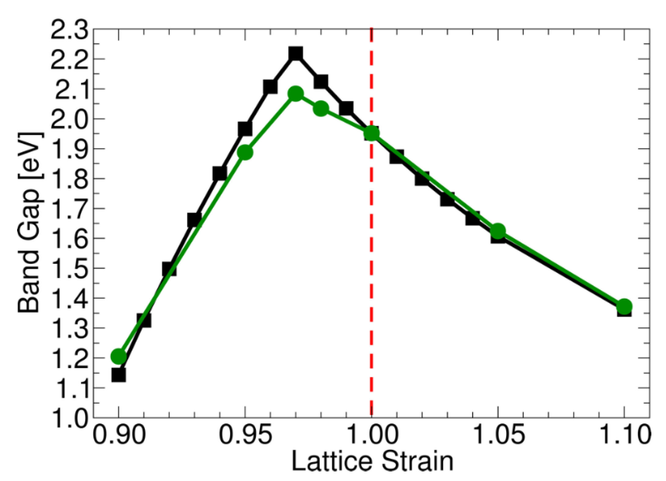
  34. Visibile, A.; Wang, R.B.; Vertova, A.; Rondinini, S.; Minguzzi, A.; Ahlberg, E.; Busch, M. Influence of Strain on the Band Gap of Cu2O. Chem. Mater. 2019, 31, 4787–4792. [Google Scholar] [CrossRef] [Green Version]
  35. Visibile, A.; Vertova, A.; Rondinini, S.; Minguzzi, A.; Ahlberg, E.; Busch, M. Strain or Electronic Effects?—The influence of alkali metals on the bandgap of Cu2O. Chem. Phys. Lett. 2020, 755, 137799. [Google Scholar] [CrossRef]
  36. Li, Y.; Zhang, X.; Chen, H.; Li, Y. Thermal conversion synthesis of Cu2O photocathode and the promoting effects of carbon coating. Catal. Commun. 2015, 66, 1–5. [Google Scholar] [CrossRef]
  37. Musa, A.; Akomolafe, T.; Carter, M. Production of cuprous oxide, a solar cell material, by thermal oxidation and a study of its physical and electrical properties. Sol. Energy Mater. Sol. Cells 1998, 51, 305–316. [Google Scholar] [CrossRef]
  38. Hsu, Y.K.; Yu, C.H.; Chen, Y.C.; Lin, Y.G. Fabrication of coral-like Cu2O nanoelectrode for solar hydrogen generation. J. Power Sources 2013, 242, 541–547. [Google Scholar] [CrossRef]
  39. Luo, J.; Steier, L.; Son, M.; Schreier, M.; Mayer, M.T.; Gra, M. Cu2O Nanowire Photocathodes for Efficient and Durable Solar Water Splitting. Nano Lett. 2016, 16, 1848–1857. [Google Scholar] [CrossRef]
  40. Wan, L.; Wang, Z.; Yang, Z.; Luo, W.; Li, Z.; Zou, Z. Modulation of dendrite growth of cuprous oxide by electrodeposition. J. Cryst. Growth 2010, 312, 3085–3090. [Google Scholar] [CrossRef]
  41. Stareck, J.E. Decorating Metals. U.S. Patents 2,081,121A, 18 May 1937. [Google Scholar]
  42. Ng, S.Y.; Ngan, A.H.W. Fabrication of nanometer-to-micron sized Cu2O single crystals by electrodeposition. Electrochim. Acta 2011, 56, 7686–7695. [Google Scholar] [CrossRef]
  43. Hu, F.; Chan, K.C.; Yue, T.M.; Surya, C. Electrochemical synthesis of transparent nanocrystalline Cu2O films using a reverse potential waveform. Thin Solid Films 2014, 550, 17–21. [Google Scholar] [CrossRef]
  44. de Jongh, P.E.; Vanmaekelbergh, D.; Kelly, J.J. Cu2O: Electrodeposition and Characterization. Chem. Mater. 1999, 11, 3512–3517. [Google Scholar] [CrossRef]
  45. Mao, Y.; He, J.; Sun, X.; Li, W.; Lu, X.; Gan, J.; Liu, Z.; Gong, L.; Chen, J.; Liu, P.; et al. Electrochemical synthesis of hierarchical Cu2O stars with enhanced photoelectrochemical properties. Electrochim. Acta 2012, 62, 1–7. [Google Scholar] [CrossRef]
  46. Zhao, W.; Fu, W.; Yang, H.; Tian, C.; Ge, R.; Wang, C.; Liu, Z.; Zhang, Y.; Li, M.; Li, Y. Shape-controlled synthesis of Cu2O microcrystals by electrochemical method. Appl. Surf. Sci. 2010, 256, 2269–2275. [Google Scholar] [CrossRef]
  47. Daltin, A.L.; Bohr, F.; Chopart, J.P. Kinetics of Cu2O electrocrystallization under magnetic fields. Electrochim. Acta 2009, 54, 5813–5817. [Google Scholar] [CrossRef]
  48. Paracchino, A.; Laporte, V.; Sivula, K.; Grätzel, M.; Thimsen, E. Highly active oxide photocathode for photoelectrochemical water reduction. Nat. Mater. 2011, 10, 456–461. [Google Scholar] [CrossRef]
  49. Paracchino, A.; Brauer, J.C.; Moser, J.-E.; Thimsen, E.; Graetzel, M. Synthesis and Characterization of High-Photoactivity Electrodeposited Cu2O Solar Absorber by Photoelectrochemistry and Ultrafast Spectroscopy. J. Phys. Chem. C 2012, 116, 7341–7350. [Google Scholar] [CrossRef] [Green Version]
  50. Lin, C.; Lai, Y.; Mersch, D.; Reisner, E. Cu2O|NiOx nanocomposite as an inexpensive photocathode in photoelectrochemical water splitting. Chem. Sci. 2012, 3, 3482–3487. [Google Scholar] [CrossRef]
  51. Golden, T.D.; Shumsky, M.G.; Zhou, Y.; VanderWerf, R.A.; Van Leeuwen, R.A.; Switzer, J.A. Electrochemical Deposition of Copper(I) Oxide Films. Chem. Mater. 1996, 8, 2499–2504. [Google Scholar] [CrossRef] [Green Version]
  52. Nian, J.N.; Hu, C.C.; Teng, H. Electrodeposited p-type Cu2O for H2 evolution from photoelectrolysis of water under visible light illumination. Int. J. Hydrog. Energy 2008, 33, 2897–2903. [Google Scholar] [CrossRef]
  53. Visibile, A.; Fracchia, M.; Baran, T.; Vertova, A.; Ghigna, P.; Ahlberg, E.; Rondinini, S.; Minguzzi, A. Electrodeposited Cu thin layers as low cost and effective underlayers for Cu2O photocathodes in photoelectrochemical water electrolysis. J. Solid State Electrochem. 2019. [Google Scholar] [CrossRef]
  54. Mahalingam, T.; Chitra, J.S.P.; Chu, J.P.; Sebastian, P.J. Preparation and microstructural studies of electrodeposited Cu2O thin films. Mater. Lett. 2004, 58, 1802–1807. [Google Scholar] [CrossRef]
  55. Wu, G.; Zhai, W.; Sun, F.; Chen, W.; Pan, Z.; Li, W. Morphology-controlled electrodeposition of Cu2O microcrystalline particle films for application in photocatalysis under sunlight. Mater. Res. Bull. 2012, 47, 4026–4030. [Google Scholar] [CrossRef]
  56. Yang, H.; Ouyang, J.; Tang, A.; Xiao, Y.; Li, X.; Dong, X.; Yu, Y. Electrochemical synthesis and photocatalytic property of cuprous oxide nanoparticles. Mater. Res. Bull. 2006, 41, 1310–1318. [Google Scholar] [CrossRef]
  57. Qiu, H.; Lu, L.; Huang, X.; Qu, Y. Facile preparation of Cu2O microcrystals with morphologies of octahedron, half circular and rectangular plates by anodic dissolution of bulk Cu in alkaline aqueous solutions. Electrochim. Acta 2010, 56, 291–296. [Google Scholar] [CrossRef]
  58. Song, H.C.; Cho, Y.S.; Huh, Y.D. Morphology-controlled synthesis of Cu2O microcrystal. Mater. Lett. 2008, 62, 1734–1736. [Google Scholar] [CrossRef]
  59. Huang, L.; Peng, F.; Yu, H.; Wang, H. Synthesis of Cu2O nanoboxes, nanocubes and nanospheres by polyol process and their adsorption characteristic. Mater. Res. Bull. 2008, 43, 3047–3053. [Google Scholar] [CrossRef]
  60. Ma, L.L.; Li, J.L.; Sun, H.Z.; Qiu, M.Q.; Wang, J.B.; Chen, J.Y.; Yu, Y. Self-assembled Cu2O flowerlike architecture: Polyol synthesis, photocatalytic activity and stability under simulated solar light. Mater. Res. Bull. 2010, 45, 961–968. [Google Scholar] [CrossRef]
  61. Zhu, J.; Wang, Y.; Wang, X.; Yang, X.; Lu, L. A convenient method for preparing shape-controlled nanocrystalline Cu2O in a polyol or water/polyol system. Powder Technol. 2008, 181, 249–254. [Google Scholar] [CrossRef]
  62. Huang, X.W.; Liu, Z.J.; Zheng, Y.F. Synthesis of Cu2O nanobelts via surfactant-assisted polyol method. Chinese Chem. Lett. 2011, 22, 879–882. [Google Scholar] [CrossRef]
  63. Bai, Y.; Yang, T.; Gu, Q.; Cheng, G.; Zheng, R. Shape control mechanism of cuprous oxide nanoparticles in aqueous colloidal solutions. Powder Technol. 2012, 227, 35–42. [Google Scholar] [CrossRef]
  64. Shin, H.S.; Song, J.Y.; Yu, J. Template-assisted electrochemical synthesis of cuprous oxide nanowires. Mater. Lett. 2009, 63, 397–399. [Google Scholar] [CrossRef]
  65. Dodoo-Arhin, D.; Leoni, M.; Scardi, P.; Garnier, E.; Mittiga, A. Synthesis, characterisation and stability of Cu2O nanoparticles produced via reverse micelles microemulsion. Mater. Chem. Phys. 2010, 122, 602–608. [Google Scholar] [CrossRef]
  66. Grez, P.; Herrera, F.; Riveros, G.; Henríquez, R.; Ramírez, A.; Muñoz, E.; Dalchiele, E.A.; Celedón, C.; Schrebler, R. Synthesis and characterization of p-Cu2O nanowires arrays. Mater. Lett. 2013, 92, 413–416. [Google Scholar] [CrossRef]
  67. Wang, Y.Q.; Liang, W.S.; Satti, A.; Nikitin, K. Fabrication and microstructure of Cu2O nanocubes. J. Cryst. Growth 2010, 312, 1605–1609. [Google Scholar] [CrossRef]
  68. Zhang, H.; Cui, Z. Solution-phase synthesis of smaller cuprous oxide nanocubes. Mater. Res. Bull. 2008, 43, 1583–1589. [Google Scholar] [CrossRef]
  69. Zhu, J.; Bi, H.; Wang, Y.; Wang, X.; Yang, X.; Lu, L. Solution-phase synthesis of Cu2O cubes using CuO as a precursor. Mater. Lett. 2008, 62, 2081–2083. [Google Scholar] [CrossRef]
  70. Zhang, X.; Cui, Z. One-pot growth of Cu2O concave octahedron microcrystal in alkaline solution. Mater. Sci. Eng. B Solid-State Mater. Adv. Technol. 2009, 162, 82–86. [Google Scholar] [CrossRef]
  71. Liang, Z.H.; Zhu, Y.J. Synthesis of uniformly sized Cu2O crystals with star-like and flower-like morphologies. Mater. Lett. 2005, 59, 2423–2425. [Google Scholar] [CrossRef]
  72. Kuo, C.H.; Huang, M.H. Morphologically controlled synthesis of Cu2O nanocrystals and their properties. Nano Today 2010, 5, 106–116. [Google Scholar] [CrossRef]
  73. Luo, Y.; Tu, Y.; Ren, Q.; Dai, X.; Xing, L.; Li, J. Surfactant-free fabrication of Cu2O nanosheets from Cu colloids and their tunable optical properties. J. Solid State Chem. 2009, 182, 182–186. [Google Scholar] [CrossRef]
  74. Wang, H.; He, S.; Yu, S.; Shi, T.; Jiang, S. Template-free synthesis of Cu2O hollow nanospheres and their conversion into Cu hollow nanospheres. Powder Technol. 2009, 193, 182–186. [Google Scholar] [CrossRef]
  75. Sui, Y.; Zhang, Y.; Fu, W.; Yang, H.; Zhao, Q.; Sun, P.; Ma, D.; Yuan, M.; Li, Y.; Zou, G. Low-temperature template-free synthesis of Cu2O hollow spheres. J. Cryst. Growth 2009, 311, 2285–2290. [Google Scholar] [CrossRef]
  76. Wei, M.; Huo, J. Preparation of Cu2O nanorods by a simple solvothermal method. Mater. Chem. Phys. 2010, 121, 291–294. [Google Scholar] [CrossRef]
  77. Wei, M.; Lun, N.; Ma, X.; Wen, S. A simple solvothermal reduction route to copper and cuprous oxide. Mater. Lett. 2007, 61, 2147–2150. [Google Scholar] [CrossRef]
  78. Lim, Y.-F.; Chua, C.S.; Lee, C.J.J.; Chi, D. Sol–gel deposited Cu2O and CuO thin films for photocatalytic water splitting. Phys. Chem. Chem. Phys. 2014, 16, 25928–25934. [Google Scholar] [CrossRef] [PubMed]
  79. Qu, Y.; Li, X.; Chen, G.; Zhang, H.; Chen, Y. Synthesis of Cu2O nano-whiskers by a novel wet-chemical route. Mater. Lett. 2008, 62, 886–888. [Google Scholar] [CrossRef]
  80. Susman, M.D.; Feldman, Y.; Vaskevich, A.; Rubinstein, I. Chemical Deposition of Cu2O Nanocrystals with Precise Morphology Control. ACS Nano 2014, 8, 162–174. [Google Scholar] [CrossRef]
  81. Balamurugan, B.; Mehta, B.R. Optical and structural properties of nanocrystalline copper oxide thin films prepared by activated reactive evaporation. Thin Solid Films 2001, 396, 90–96. [Google Scholar] [CrossRef]
  82. Al-Kuhaili, M.F. Characterization of copper oxide thin films deposited by the thermal evaporation of cuprous oxide (Cu2O). Vacuum 2008, 82, 623–629. [Google Scholar] [CrossRef]
  83. Barreca, D.; Comini, E.; Gasparotto, A.; Maccato, C.; Sada, C.; Sberveglieri, G.; Tondello, E. Chemical vapor deposition of copper oxide films and entangled quasi-1D nanoarchitectures as innovative gas sensors. Sensors Actuators, B Chem. 2009, 141, 270–275. [Google Scholar] [CrossRef]
  84. Wang, S.; Zhang, X.; Pan, L.; Zhao, F.-M.; Zou, J.-J.; Zhang, T.; Wang, L. Controllable sonochemical synthesis of Cu2O/Cu2(OH)3NO3 composites toward synergy of adsorption and photocatalysis. Appl. Catal. B Environ. 2015, 164, 234–240. [Google Scholar] [CrossRef]
  85. Ma, D.; Liu, H.; Yang, H.; Fu, W.; Zhang, Y.; Yuan, M.; Sun, P.; Zhou, X. High pressure hydrothermal synthesis of cuprous oxide microstructures of novel morphologies. Mater. Chem. Phys. 2009, 116, 458–463. [Google Scholar] [CrossRef]
  86. Valodkar, M.; Pal, A.; Thakore, S. Synthesis and characterization of cuprous oxide dendrites: New simplified green hydrothermal route. J. Alloys Compd. 2011, 509, 523–528. [Google Scholar] [CrossRef]
  87. Togashi, T.; Hitaka, H.; Ohara, S.; Naka, T.; Takami, S.; Adschiri, T. Controlled reduction of Cu2+ to Cu+ with an N,O-type chelate under hydrothermal conditions to produce Cu2O nanoparticles. Mater. Lett. 2010, 64, 1049–1051. [Google Scholar] [CrossRef]
  88. Neskovska, R.; Ristova, M.; Velevska, J.; Ristov, M. Electrochromism of the electroless deposited cuprous oxide films. Thin Solid Films 2007, 515, 4717–4721. [Google Scholar] [CrossRef]
  89. Itoh, T.; Maki, K. Growth process of CuO(111) and Cu2O(001) thin films on MgO(001) substrate under metal-mode condition by reactive dc-magnetron sputtering. Vacuum 2007, 81, 1068–1076. [Google Scholar] [CrossRef]
  90. Nolan, M. Defects in Cu2O, CuAlO2 and SrCu2O2 transparent conducting oxides. Thin Solid Films 2008, 516, 8130–8135. [Google Scholar] [CrossRef]
  91. Li, M.; Zhang, J.-Y.; Zhang, Y.; Wang, T.-M. Oxygen vacancy in N-doped Cu2O crystals: A density functional theory study. Chin. Phys. B 2012, 21, 087301. [Google Scholar] [CrossRef]
  92. Martínez-Ruiz, A.; Moren, M.G.; Takeuchi, N. First principles calculations of the electronic properties of bulk Cu2O, clean and doped with Ag, Ni, and Zn. Solid State Sci. 2003, 5, 291–295. [Google Scholar] [CrossRef]
  93. Kleinman, L.; Mednick, K. Self-consistent energy bands of Cu2O. Phys. Rev. B 1980, 21, 1549–1553. [Google Scholar] [CrossRef]
  94. Mahalingam, T.; Chitra, J.S.P.; Chu, J.P. Structural and annealing studies of potentiostatically deposited Cu2O thin films. Sol. Energy Mater. Sol. Cells 2005, 88, 209–216. [Google Scholar] [CrossRef]
  95. Liang, R.; Chang, Y.; Wu, P.; Lin, P. Effect of annealing on the electrodeposited Cu2O fi lms for photoelectrochemical hydrogen generation. Thin Solid Films 2010, 518, 7191–7195. [Google Scholar] [CrossRef]
  96. Jin, C.; Baek, K.; Park, S.; Kim, H.W.; Lee, W.I.; Lee, C. Influence of coating and thermal annealing on the structure and luminescence properties of CuO nanorods. Solid State Commun. 2010, 150, 1812–1817. [Google Scholar] [CrossRef]
  97. Nolan, M.; Elliott, S.D. Tuning the electronic structure of the transparent conducting oxide Cu2O. Thin Solid Films 2008, 516, 1468–1472. [Google Scholar] [CrossRef]
  98. Mittal, A.; Mari, B.; Sharma, S.; Kumari, V.; Maken, S.; Kumari, K.; Kumar, N. Non-metal modified TiO2: A step towards visible light photocatalysis. J. Mater. Sci. Mater. Electron. 2019, 30, 3186–3207. [Google Scholar] [CrossRef]
  99. Wan, H.; Xu, L.; Huang, W.Q.; Huang, G.F.; He, C.N.; Zhou, J.H.; Peng, P. Band engineering of ZnS by codoping for visible-light photocatalysis. Appl. Phys. A Mater. Sci. Process. 2014, 116, 741–750. [Google Scholar] [CrossRef]
  100. Chen, Y.Y.; Duh, J.G.; Chiou, B.S.; Peng, C.G. Luminescent mechanisms of ZnS:Cu:Cl and ZnS:Cu:Al phosphors. Thin Solid Films 2001, 392, 50–55. [Google Scholar] [CrossRef]
  101. Tsur, Y.; Riess, I. Self-compensation in semiconductors. Phys. Rev. B 1999, 60, 8138–8146. [Google Scholar] [CrossRef]
  102. Han, X.; Han, K.; Tao, M. n-Type Cu2O by Electrochemical Doping with Cl. Electrochem. Solid-State Lett. 2009, 12, H89–H91. [Google Scholar] [CrossRef]
  103. Scanlon, D.O.; Watson, G.W. Undoped n-Type Cu2O: Fact or Fiction? J. Phys. Chem. Lett. 2010, 1, 2582–2585. [Google Scholar] [CrossRef]
  104. Scanlon, D.O.; Morgan, B.J.; Watson, G.W.; Walsh, A. Acceptor levels in p-type Cu2O: Rationalizing theory and Experiment. Phys. Rev. Lett. 2009, 103, 1–4. [Google Scholar] [CrossRef] [PubMed]
  105. Biccari, F.; Malerba, C.; Mittiga, A. Chlorine doping of Cu2O. Sol. Energy Mater. Sol. Cells 2010, 94, 1947–1952. [Google Scholar] [CrossRef]
  106. Soon, A.; Wallman, J.; Delley, B.; Stampfl, C. Early transition metal dopants in cuprous oxide: To spin or not to spin. Curr. Appl. Phys. 2013, 13, 1707–1712. [Google Scholar] [CrossRef]
  107. Kudo, A.; Yanagi, H.; Hosono, H.; Kawazoe, H. SrCu2O2: A p-type conductive oxide with wide band gap. Appl. Phys. Lett. 1998, 73, 220–222. [Google Scholar] [CrossRef]
  108. Tabuchi, N.; Matsumura, H. Control of carrier concentration in thin cuprous oxide Cu2O films by atomic hydrogen. Japanese J. Appl. Phys. Part 1 Regul. Pap. Short Notes Rev. Pap. 2002, 41, 5060–5063. [Google Scholar] [CrossRef]
  109. Akimoto, K.; Ishizuka, S.; Yanagita, M.; Nawa, Y.; Paul, G.K.; Sakurai, T. Thin film deposition of Cu2O and application for solar cells. Sol. Energy 2006, 80, 715–722. [Google Scholar] [CrossRef]
  110. Caballero-Briones, F.; Palacios-Padrós, A.; Calzadilla, O.; Moreira, I.D.P.R.; Sanz, F. Disruption of the chemical environment and electronic structure in p-type Cu2O films by alkaline doping. J. Phys. Chem. C 2012, 116, 13524–13535. [Google Scholar] [CrossRef]
  111. Elfadill, N.G.; Hashim, M.R.; Chahrour, K.M.; Mohammed, S.A. Electrochemical deposition of Na-doped p-type Cu2O film on n-type Si for photovoltaic application. J. Electroanal. Chem. 2016, 767, 7–12. [Google Scholar] [CrossRef]
  112. Minami, T.; Nishi, Y.; Miyata, T. Impact of incorporating sodium into polycrystalline p-type Cu2O for heterojunction solar cell applications. Appl. Phys. Lett. 2014, 105, 212104. [Google Scholar] [CrossRef]
  113. Elfadill, N.G.; Hashim, M.R.; Chahrour, K.M.; Mohammed, S.A. Preparation of p-type Na-doped Cu2O by electrodeposition for a p-n homojunction thin film solar cell. Semicond. Sci. Technol. 2016, 31, 065001. [Google Scholar] [CrossRef]
  114. Zhao, Z.; He, X.; Yi, J.; Ma, C.; Cao, Y.; Qiu, J. First-principles study on the doping effects of nitrogen on the electronic structure and optical properties of Cu2O. RSC Adv. 2013, 3, 84–90. [Google Scholar] [CrossRef]
  115. Zou, M.; Liu, H.; Feng, L.; Thomas, T.; Yang, M. Enhanced visible light photocatalytic activity in N-doped edge- and corner-truncated octahedral Cu2O. Solid State Sci. 2017, 65, 22–28. [Google Scholar] [CrossRef]
  116. Ping, Z.; Yurong, Z.; Qingbo, Y.; Fengzhen, L. A combined experimental-computational study on nitrogen doped Cu2O as the wide-spectrum absorption material. J. Semicond. 2014, 35, 103001. [Google Scholar] [CrossRef]
  117. Siah, S.C.; Lee, Y.S.; Brandt, R.; Buonassisi, T. Low-resistance earth-abundant metal contacts to nitrogen-doped cuprous oxide thin films. In Proceedings of the 2012 38th IEEE Photovoltaic Specialists Conference, Austin, TX, USA, 3–8 June 2012; pp. 2605–2607. [Google Scholar] [CrossRef]
  118. Ye, F.; Su, X.Q.; Cai, X.M.; Zheng, Z.H.; Liang, G.X.; Zhang, D.P.; Luo, J.T.; Fan, P. The electrical and thermoelectric properties of Zn-doped cuprous oxide. Thin Solid Films 2016, 603, 395–399. [Google Scholar] [CrossRef]
  119. Zhang, L.; Jing, D.; Guo, L.; Yao, X. In Situ Photochemical Synthesis of Zn-Doped Cu2O Hollow Microcubes for High Efficient Photocatalytic H2 Production. ACS Sustain. Chem. Eng. 2014, 2, 1446–1452. [Google Scholar] [CrossRef]
  120. Cai, X.M.; Su, X.Q.; Ye, F.; Zhang, D.P.; Luo, J.T.; Fan, P.; Zheng, Z.H.; Liang, G.X.; Roy, V.A.L.; Xiao, J.J. Fabrication and properties of pure-phase Cu2O co-doped with zinc and indium. J. Alloys Compd. 2017, 697, 5–10. [Google Scholar] [CrossRef]
  121. Hu, F.; Zou, Y.; Wang, L.; Wen, Y.; Xiong, Y. Photostable Cu2O photoelectrodes fabricated by facile Zn-doping electrodeposition. Int. J. Hydrog. Energy 2016, 41, 15172–15180. [Google Scholar] [CrossRef]
  122. Heng, B.; Xiao, T.; Tao, W.; Hu, X.; Chen, X.; Wang, B.; Sun, D.; Tang, Y. Zn doping-induced shape evolution of microcrystals: The case of cuprous oxide. Cryst. Growth Des. 2012, 12, 3998–4005. [Google Scholar] [CrossRef]
  123. Ishizuka, S.; Kato, S.; Okamoto, Y.; Akimoto, K. Control of hole carrier density of polycrystalline Cu2O thin films by Si doping. Appl. Phys. Lett. 2002, 80, 950–952. [Google Scholar] [CrossRef]
  124. Upadhyay, S.; Sharma, D.; Singh, N.; Satsangi, V.R.; Shrivastav, R.; Waghmare, U.V.; Dass, S. Experimental and first-principles theoretical studies on Ag-doped cuprous oxide as photocathode in photoelectrochemical splitting of water. J. Mater. Sci. 2014, 49, 868–876. [Google Scholar] [CrossRef]
  125. Upadhyay, S.; Sharma, D.; Satsangi, V.R.; Shrivastav, R.; Waghmare, U.V.; Dass, S. Spray pyrolytically deposited Fe-doped Cu2O thin films for solar hydrogen generation: Experiments & first-principles analysis. Mater. Chem. Phys. 2015, 160, 32–39. [Google Scholar] [CrossRef]
  126. Joseph, D.P.; David, T.P.; Raja, S.P.; Venkateswaran, C. Phase stabilization and characterization of nanocrystalline Fe-doped Cu2O. Mater. Charact. 2008, 59, 1137–1139. [Google Scholar] [CrossRef]
  127. Jiang, Z.-Q.; Yao, G.; An, X.-Y.; Fu, Y.-J.; Cao, L.-H.; Wu, W.-D.; Wang, X.-M. Electronic and optical properties of Au-doped Cu2O: A first principles investigation. Chin. Phys. B 2014, 23, 057104. [Google Scholar] [CrossRef]
  128. Resende, J.; Jiménez, C.; Nguyen, N.D.; Deschanvres, J.-L. Magnesium-doped cuprous oxide (Mg:Cu2O) thin films as a transparent p-type semiconductor. Phys. Status Solidi 2016, 7, 2296–2302. [Google Scholar] [CrossRef]
  129. Kardarian, K.; Nunes, D.; Maria Sberna, P.; Ginsburg, A.; Keller, D.A.; Vaz Pinto, J.; Deuermeier, J.; Anderson, A.Y.; Zaban, A.; Martins, R.; et al. Effect of Mg doping on Cu2O thin films and their behavior on the TiO2/Cu2O heterojunction solar cells. Sol. Energy Mater. Sol. Cells 2016, 147, 27–36. [Google Scholar] [CrossRef]
  130. Brochen, S.; Bergerot, L.; Favre, W.; Resende, J.; Jiménez, C.; Deschanvres, J.-L.; Consonni, V. Effect of Strontium Incorporation on the p-Type Conductivity of Cu2O Thin Films Deposited by Metal–Organic Chemical Vapor Deposition. J. Phys. Chem. C 2016, 120, 17261–17267. [Google Scholar] [CrossRef]
  131. Bergerot, L.; Jiménez, C.; Chaix-Pluchery, O.; Rapenne, L.; Deschanvres, J.-L. Growth and characterization of Sr-doped Cu2O thin films deposited by metalorganic chemical vapor deposition. Phys. Status Solidi 2015, 212, 1735–1741. [Google Scholar] [CrossRef]
  132. Pan, L.; Zhu, H.; Fan, C.; Wang, W.; Zhang, Y.; Xiao, J.Q. Mn-doped Cu2O thin films grown by rf magnetron sputtering. J. Appl. Phys. 2005, 97, 10D318. [Google Scholar] [CrossRef]
  133. Wei, M.; Braddon, N.; Zhi, D.; Midgley, P.A.; Chen, S.K.; Blamire, M.G.; MacManus-Driscoll, J.L. Room temperature ferromagnetism in bulk Mn-Doped Cu2O. Appl. Phys. Lett. 2005, 86, 1–3. [Google Scholar] [CrossRef]
  134. Kikuchi, N.; Tonooka, K. Electrical and structural properties of Ni-doped Cu2O films prepared by pulsed laser deposition. Thin Solid Films 2005, 486, 33–37. [Google Scholar] [CrossRef]
  135. Zhang, J.; Tse, K.; Wong, M.; Zhang, Y.; Zhu, J. A brief review of co-doping. Front. Phys. 2016, 11. [Google Scholar] [CrossRef] [Green Version]
  136. Lin, Y.; Jiang, Z.; Zhang, R.; Zhu, C.; Hu, X.; Zhang, X.; Zhu, H. The structure, electronic, and optical properties of (Sm,N)-codoped anatase TiO2 photocatalyst: A density functional study. J. Catal. 2014, 309, 115–120. [Google Scholar] [CrossRef]
  137. Muruganandham, M.; Kusumoto, Y. Synthesis of N, C codoped hierarchical porous microsphere ZnS as a visible light-responsive photocatalyst. J. Phys. Chem. C 2009, 113, 16144–16150. [Google Scholar] [CrossRef]
  138. Huang, H.; Liu, K.; Chen, K.; Zhang, Y.; Zhang, Y.; Wang, S. Ce and F comodification on the crystal structure and enhanced photocatalytic activity of Bi2WO6 photocatalyst under visible light irradiation. J. Phys. Chem. C 2014, 118, 14379–14387. [Google Scholar] [CrossRef]
  139. Luque, A.; Martí, A. Increasing the Efficiency of Ideal Solar Cells by Photon Induced Transitions at Intermediate Levels. Phys. Rev. Lett. 1997, 78, 5014–5017. [Google Scholar] [CrossRef]
  140. Luque, A.; Martí, A.; Antolín, E.; Tablero, C. Intermediate bands versus levels in non-radiative recombination. Phys. B Condens. Matter 2006, 382, 320–327. [Google Scholar] [CrossRef]
  141. Palacios, P.; Sánchez, K.; Conesa, J.C.; Fernández, J.J.; Wahnón, P. Theoretical modelling of intermediate band solar cell materials based on metal-doped chalcopyrite compounds. Thin Solid Films 2007, 515, 6280–6284. [Google Scholar] [CrossRef] [Green Version]
  142. Palacios, P.; Aguilera, I.; Sánchez, K.; Conesa, J.C.; Wahnón, P. Transition-metal-substituted indium thiospinels as novel intermediate-band materials: Prediction and understanding of their electronic properties. Phys. Rev. Lett. 2008, 101, 2–5. [Google Scholar] [CrossRef] [Green Version]
  143. López, N.; Reichertz, L.A.; Yu, K.M.; Campman, K.; Walukiewicz, W. Engineering the electronic band structure for multiband solar cells. Phys. Rev. Lett. 2011, 106, 028701. [Google Scholar] [CrossRef]
  144. Luque, A.; Martí, A.; Cuadra, L. Thermodynamic consistency of sub-bandgap absorbing solar cell proposals. IEEE Trans. Electron Devices 2001, 48, 2118–2124. [Google Scholar] [CrossRef]
  145. Okada, Y.; Ekins-Daukes, N.J.; Kita, T.; Tamaki, R.; Yoshida, M.; Pusch, A.; Hess, O.; Phillips, C.C.; Farrell, D.J.; Yoshida, K.; et al. Intermediate band solar cells: Recent progress and future directions. Cit. Appl. Phys. Rev. Appl. Phys. Lett 2015, 2, 21302–233510. [Google Scholar] [CrossRef] [Green Version]
  146. Luque, A.; Martí, A.; Stanley, C.; López, N.; Cuadra, L.; Zhou, D.; Pearson, J.L.; McKee, A. General equivalent circuit for intermediate band devices: Potentials, currents and electroluminescence. J. Appl. Phys. 2004, 96, 903–909. [Google Scholar] [CrossRef]
  147. Palacios, P.; Sánchez, K.; Wahnón, P.; Conesa, J.C. Characterization by Ab Initio Calculations of an Intermediate Band Material Based on Chalcopyrite Semiconductors Substituted by Several Transition Metals. J. Sol. Energy Eng. 2007, 129, 314. [Google Scholar] [CrossRef]
  148. Malerba, C.; Azanza Ricardo, C.L.; Dincau, M.; Biccari, F.; Scardi, P.; Mittiga, A. Nitrogen doped Cu2O: A possible material for intermediate band solar cells? Sol. Energy Mater. Sol. Cells 2012, 105, 192–195. [Google Scholar] [CrossRef]
  149. Jang, Y.J.; Park, Y.B.; Kim, H.E.; Choi, Y.H.; Choi, S.H.; Lee, J.S. Oxygen-Intercalated CuFeO2 Photocathode Fabricated by Hybrid Microwave Annealing for Efficient Solar Hydrogen Production. Chem. Mater. 2016, 28, 6054–6061. [Google Scholar] [CrossRef]
  150. Luque, A.; Martí, A. A metallic intermediate band high efficiency solar cell. Prog. Photovoltaics Res. Appl. 2001, 9, 73–86. [Google Scholar] [CrossRef]
  151. Palacios, P.; Sánchez, K.; Conesa, J.C.; Wahnón, P. First principles calculation of isolated intermediate bands formation in a transition metal-doped chalcopyrite-type semiconductor. Phys. Status Solidi Appl. Mater. Sci. 2006, 203, 1395–1401. [Google Scholar] [CrossRef]
  152. Luque, A.; Martí, A.; Stanley, C. Understanding intermediate-band solar cells. Nat. Photonics 2012, 6, 146–152. [Google Scholar] [CrossRef] [Green Version]
  153. Aguilera, I.; Palacios, P.; Wahnón, P. Understanding Ti intermediate-band formation in partially inverse thiospinel MgIn2S4 through many-body approaches. Phys. Rev. B Condens. Matter Mater. Phys. 2011, 84, 1–6. [Google Scholar] [CrossRef] [Green Version]
  154. Zhao, Q.M.; Zhao, Z.Y.; Liu, Q.L.; Yao, G.Y.; Dong, X.D. Delafossite CuGaO2 as promising visible-light-driven photocatalyst: Synthesize, properties, and performances. J. Phys. D. Appl. Phys. 2020, 53, 135102. [Google Scholar] [CrossRef]
  155. Prévot, M.S.; Guijarro, N.; Sivula, K. Enhancing the Performance of a Robust Sol-Gel-Processed p-Type Delafossite CuFeO2 Photocathode for Solar Water Reduction. ChemSusChem 2015, 8, 1359–1367. [Google Scholar] [CrossRef]
  156. Prévot, M.S.; Jeanbourquin, X.A.; Bourée, W.S.; Abdi, F.; Friedrich, D.; Van De Krol, R.; Guijarro, N.; Le Formal, F.; Sivula, K. Evaluating Charge Carrier Transport and Surface States in CuFeO2 Photocathodes. Chem. Mater. 2017, 29, 4952–4962. [Google Scholar] [CrossRef]
  157. Zhao, R.D.; Zhang, Y.M.; Liu, Q.L.; Zhao, Z.Y. Effects of the Preparation Process on the Photocatalytic Performance of Delafossite CuCrO2. Inorg. Chem. 2020, 59, 16679–16689. [Google Scholar] [CrossRef]
  158. Choi, S.Y.; Kim, C.D.; Han, D.S.; Park, H. Facilitating hole transfer on electrochemically synthesized p-type CuAlO2 films for efficient solar hydrogen production from water. J. Mater. Chem. A 2017, 5, 10165–10172. [Google Scholar] [CrossRef] [Green Version]
  159. Gu, J.; Yan, Y.; Krizan, J.W.; Gibson, Q.D.; Detweiler, Z.M.; Cava, R.J.; Bocarsly, A.B. P-type CuRhO2 as a self-healing photoelectrode for water reduction under visible light. J. Am. Chem. Soc. 2014, 136, 830–833. [Google Scholar] [CrossRef]
  160. Berglund, S.P.; Abdi, F.F.; Bogdanoff, P.; Chemseddine, A.; Friedrich, D.; Van De Krol, R. Comprehensive Evaluation of CuBi2O4 as a Photocathode Material for Photoelectrochemical Water Splitting. Chem. Mater. 2016, 28, 4231–4242. [Google Scholar] [CrossRef]
  161. Rajeshwar, K.; Hossain, M.K.; Macaluso, R.T.; Janáky, C.; Varga, A.; Kulesza, P.J. Review—Copper Oxide-Based Ternary and Quaternary Oxides: Where Solid-State Chemistry Meets Photoelectrochemistry. J. Electrochem. Soc. 2018, 165, H3192–H3206. [Google Scholar] [CrossRef]
  162. Park, S.; Baek, J.H.; Zhang, L.; Lee, J.M.; Stone, K.H.; Cho, I.S.; Guo, J.; Jung, H.S.; Zheng, X. Rapid Flame-Annealed CuFe2O4 as Efficient Photocathode for Photoelectrochemical Hydrogen Production. ACS Sustain. Chem. Eng. 2019, 7, 5867–5874. [Google Scholar] [CrossRef]
  163. Liu, H.; Nakamura, R.; Nakato, Y. Bismuth-copper vanadate BiCu2VO6 as a novel photocatalyst for efficient visible-light-driven oxygen evolution. ChemPhysChem 2005, 6, 2499–2502. [Google Scholar] [CrossRef]
  164. Zhou, L.; Bainglass, E.; Masroor, M.; Giri, B.; Li, G.; Carl, A.; Grimm, R.L.; Huda, M.N.; Titova, L.V.; Rao, P.M. Synthesis and optoelectronic properties of a promising quaternary metal oxide light absorber CuBiW2O8. J. Mater. Chem. A 2021, 9, 1643–1654. [Google Scholar] [CrossRef]
  165. Biswas, S.K.; Baeg, J.O.; Kale, B.B.; Yadav, R.K.; Moon, S.J.; Kong, K.J.; So, W.W. An efficient visible-light active photocatalyst CuAlGaO 4 for solar hydrogen production. Catal. Commun. 2011, 12, 651–654. [Google Scholar] [CrossRef]
  166. Hua, E.; Jin, S.; Ni, S.; Xu, X. Double perovskite compounds A2CuWO6 (A = Sr and Ba) with p-type semiconductivity for photocatalytic water oxidation under visible light illumination. Inorg. Chem. Front. 2019, 6, 2096–2103. [Google Scholar] [CrossRef]
  167. Raizada, P.; Sudhaik, A.; Patial, S.; Hasija, V.; Parwaz Khan, A.A.; Singh, P.; Gautam, S.; Kaur, M.; Nguyen, V.-H. Engineering nanostructures of CuO-based photocatalysts for water treatment: Current progress and future challenges. Arab. J. Chem. 2020, 13, 8424–8457. [Google Scholar] [CrossRef]
  168. Kubiak, A.; Bielan, Z.; Kubacka, M.; Gabała, E.; Zgoła-Grześkowiak, A.; Janczarek, M.; Zalas, M.; Zielińska-Jurek, A.; Siwińska-Ciesielczyk, K.; Jesionowski, T. Microwave-assisted synthesis of a TiO2-CuO heterojunction with enhanced photocatalytic activity against tetracycline. Appl. Surf. Sci. 2020, 520, 146344. [Google Scholar] [CrossRef]
  169. Zhang, S.; Gong, X.; Shi, Q.; Ping, G.; Xu, H.; Waleed, A.; Li, G. CuO nanoparticle-decorated TiO2-nanotube heterojunctions for direct synthesis of methyl formate via photo-oxidation of methanol. ACS Omega 2020, 5, 15942–15948. [Google Scholar] [CrossRef]
  170. Farah, J.; Ibadurrohman, M. Slamet Synthesis of CuO-TiO2 nano-composite for formaldehyde degradation application. In AIP Conference Proceedings; AIP Publishing LLC: Melville, NY, USA, 2019; Volume 2175, p. 20044. [Google Scholar]
  171. de Brito, J.F.; Tavella, F.; Genovese, C.; Ampelli, C.; Zanoni, M.V.B.; Centi, G.; Perathoner, S. Role of CuO in the modification of the photocatalytic water splitting behavior of TiO2 nanotube thin films. Appl. Catal. B Environ. 2018, 224, 136–145. [Google Scholar] [CrossRef] [Green Version]
  172. Nuo Peh, C.K.; Wang, X.-Q.; Ho, G.W. Increased photocatalytic activity of {CuO}/{TiO2} through broadband solar absorption heating under natural sunlight. Procedia Eng. 2017, 215, 171–179. [Google Scholar] [CrossRef]
  173. Edelmannová, M.; Lin, K.Y.; Wu, J.C.S.; Troppová, I.; Čapek, L.; Kočí, K. Photocatalytic hydrogenation and reduction of CO 2 over CuO/TiO2 photocatalysts. Appl. Surf. Sci. 2018, 454, 313–318. [Google Scholar] [CrossRef]
  174. Surikanti, G.R.; Bandarapu, A.K.; Sunkara, M.V. A Facile One Pot Synthesis of Cu2O@TiO2: A Nanocomposite Catalyst for Enhanced Visible Light Driven Photocatalysis. ChemistrySelect 2019, 4, 2249–2257. [Google Scholar] [CrossRef]
  175. Trang, T.N.Q.; Tu, L.T.N.; Man, T.V.; Mathesh, M.; Nam, N.D.; Thu, V.T.H. A high-efficiency photoelectrochemistry of Cu2O/TiO2 nanotubes based composite for hydrogen evolution under sunlight. Compos. Part B Eng. 2019, 174, 106969. [Google Scholar] [CrossRef]
  176. Li, G.; Huang, J.; Chen, J.; Deng, Z.; Huang, Q.; Liu, Z.; Guo, W.; Cao, R. Highly Active Photocatalyst of Cu2O/TiO2 Octahedron for Hydrogen Generation. ACS Omega 2019, 4, 3392–3397. [Google Scholar] [CrossRef]
  177. Zhao, W.; Liu, C. Mesoporous Cu-Cu2O@TiO2 heterojunction photocatalysts derived from metal-organic frameworks. RSC Adv. 2020, 10, 14550–14555. [Google Scholar] [CrossRef] [Green Version]
  178. Liao, Y.; Deng, P.; Wang, X.; Zhang, D.; Li, F.; Yang, Q.; Zhang, H.; Zhong, Z. A Facile Method for Preparation of Cu2O-TiO2 NTA Heterojunction with Visible-Photocatalytic Activity. Nanoscale Res. Lett. 2018, 13, 221. [Google Scholar] [CrossRef]
  179. Al-Namshah, K.S. Impact of CuO incorporation on the photocatalytic enhancement of the mesostructured Fe2O3 nanocomposite. Appl. Nanosci. 2021, 11, 467–476. [Google Scholar] [CrossRef]
  180. Wojtyła, S.; Baran, T. Copper zinc oxide heterostructure nanoflowers for hydrogen evolution. Int. J. Hydrog. Energy 2019, 44. [Google Scholar] [CrossRef]
  181. Zhang, J.; Ma, H.; Liu, Z. Highly efficient photocatalyst based on all oxides WO3/Cu2O heterojunction for photoelectrochemical water splitting. Appl. Catal. B Environ. 2017, 201, 84–91. [Google Scholar] [CrossRef]
  182. Zhang, Q.; Li, Z.; Chen, S.; Zhang, Z.; Ali, S.; Jing, L. Improved photocatalytic activities of porous In2O3 with large surface area by coupling with K-modified CuO for degrading pollutants. Catal. Today 2020, 339, 403–410. [Google Scholar] [CrossRef]
  183. Wojtyła, S.; Baran, T. Electrochemically prepared copper/indium oxides photocathode for efficient photoelectrochemical hydrogen production. Sol. Energy Mater. Sol. Cells 2020, 206, 110262. [Google Scholar] [CrossRef]
  184. Wojtyła, S.; Baran, T. Copper-Nickel-Oxide Nanomaterial for Photoelectrochemical Hydrogen Evolution and Photocatalytic Degradation of Volatile Organic Compounds. Mater. Res. Bull. 2021, 142, 111418. [Google Scholar] [CrossRef]
  185. Wang, N.; Pan, Y.; Lu, T.; Li, X.; Wu, S.; Wu, J. A new ribbon-ignition method for fabricating p-CuO/n-CeO2 heterojunction with enhanced photocatalytic activity. Appl. Surf. Sci. 2017, 403, 699–706. [Google Scholar] [CrossRef]
  186. Wei, X.; Pan, J.; Wang, S.; Mei, J.; Zheng, Y.; Cui, C.; Li, C. CdS modified Cu2O octahedral nano-heterojunction and its photocatalytic application. J. Mater. Sci. Mater. Electron. 2017, 28, 14079–14084. [Google Scholar] [CrossRef]
  187. Naresh, G.; Hsieh, P.-L.; Meena, V.; Lee, S.-K.; Chiu, Y.-H.; Madasu, M.; Lee, A.-T.; Tsai, H.-Y.; Lai, T.-H.; Hsu, Y.-J.; et al. Facet-Dependent Photocatalytic Behaviors of ZnS-Decorated Cu2O Polyhedra Arising from Tunable Interfacial Band Alignment. ACS Appl. Mater. Interfaces 2019, 11, 3582–3589. [Google Scholar] [CrossRef] [PubMed]
  188. Kao, Y.-T.; Yang, S.-M.; Lu, K.-C. Synthesis and Photocatalytic Properties of CuO-CuS Core-Shell Nanowires. Materials 2019, 12, 1106. [Google Scholar] [CrossRef] [Green Version]
  189. Bisht, N.S.; Mehta, S.P.S.; Sahoo, N.G.; Dandapat, A. The room temperature synthesis of a CuO-Bi-BiOBr ternary Z-scheme photocatalyst for enhanced sunlight driven alcohol oxidation. Dalt. Trans. 2021, 50, 5001–5010. [Google Scholar] [CrossRef]
  190. Fu, J.; Cao, S.; Yu, J. Dual Z-scheme charge transfer in TiO2–Ag–Cu2O composite for enhanced photocatalytic hydrogen generation. J. Mater. 2015, 1, 124–133. [Google Scholar] [CrossRef] [Green Version]
  191. Chen, G.; Wang, H.; Wei, X.; Wu, Y.; Gu, W.; Hu, L.; Xu, D.; Zhu, C. Efficient Z-Scheme heterostructure based on TiO2/Ti3C2Tx/Cu2O to boost photoelectrochemical response for ultrasensitive biosensing. Sens. Actuators B Chem. 2020, 312, 127951. [Google Scholar] [CrossRef]
  192. Zheng, J.; Liu, X.; Zhang, L. Design of porous double-shell Cu2O@CuCo2O4 Z-Scheme hollow microspheres with superior redox property for synergistic photocatalytic degradation of multi-pollutants. Chem. Eng. J. 2020, 389, 124339. [Google Scholar] [CrossRef]
  193. Bao, Y.; Chen, K. A novel Z-scheme visible light driven Cu2O/Cu/g-C3N4 photocatalyst using metallic copper as a charge transfer mediator. Mol. Catal. 2017, 432, 187–195. [Google Scholar] [CrossRef]
  194. He, J.; Shao, D.W.; Zheng, L.C.; Zheng, L.J.; Feng, D.Q.; Xu, J.P.; Zhang, X.H.; Wang, W.C.; Wang, W.-H.; Lu, F.; et al. Construction of Z-scheme Cu2O/Cu/AgBr/Ag photocatalyst with enhanced photocatalytic activity and stability under visible light. Appl. Catal. B Environ. 2017, 203, 917–926. [Google Scholar] [CrossRef]
  195. Vidyasagar, D.; Kim, D.J.; Kim, M.G.; Bhoyar, T.; Tonda, S. Chapter 9—Development of graphitic carbon nitride-based Z-scheme photocatalysts. In Heterostructured Photocatalysts for Solar Energy Conversion; Ghosh, S., Ed.; Solar Cell Engineering; Elsevier: Amsterdam, The Netherlands, 2021; pp. 327–358. ISBN 978-0-12-820072-8. [Google Scholar]
  196. Liu, P.; Bao, R.; Fang, D.; Yi, J.; Li, L. A facile synthesis of CNTs/Cu2O-CuO heterostructure composites by spray pyrolysis and its visible light responding photocatalytic properties. Adv. Powder Technol. 2018, 29, 2027–2034. [Google Scholar] [CrossRef]
  197. Khusnun, N.F.; Jalil, A.A.; Triwahyono, S.; Hitam, C.N.C.; Hassan, N.S.; Jamian, F.; Nabgan, W.; Abdullah, T.A.T.; Kamaruddin, M.J.; Hartanto, D. Directing the amount of CNTs in CuO–CNT catalysts for enhanced adsorption-oriented visible-light-responsive photodegradation of p-chloroaniline. Powder Technol. 2018, 327, 170–178. [Google Scholar] [CrossRef]
  198. Mohd Shah, R.; Mohamad Yunus, R.; Mastar @ Masdar, M.S.; Jeffery Minggu, L.; Wong, W.Y.; Salehmin, M.N.I. High photoelectrochemical performance of a p-type reduced graphene oxide-copper oxide/Cu foil (rGO-CuO/Cu) photoelectrode prepared by a one-pot hydrothermal method. Int. J. Energy Res. 2021, 45, 13865–13877. [Google Scholar] [CrossRef]
  199. Mahdi, R.; Alsultan, M.; Al-Keisy, A.; Swiegers, G.F. Photocatalytic Hydrogen Generation from pH-Neutral Water by a Flexible Tri-Component Composite. Catal. Lett. 2021, 151, 1700–1706. [Google Scholar] [CrossRef]
  200. Kecsenovity, E.; Endrődi, B.; Tóth, P.S.; Zou, Y.; Dryfe, R.A.W.; Rajeshwar, K.; Janáky, C. Enhanced Photoelectrochemical Performance of Cuprous Oxide/Graphene Nanohybrids. J. Am. Chem. Soc. 2017, 139, 6682–6692. [Google Scholar] [CrossRef]
  201. Bhargava, R.; Khan, S. Enhanced optical properties of Cu2O anchored on reduced graphene oxide ({rGO}) sheets. J. Phys. Condens. Matter 2018, 30, 335703. [Google Scholar] [CrossRef]
  202. Zhang, D.; Yang, J.; Wang, J.; Yang, J.; Qiao, G. Construction of Cu2O-reduced graphene oxide composites with enhanced photoelectric and photocatalytic properties. Opt. Mater. 2020, 100, 109612. [Google Scholar] [CrossRef]
  203. Liu, S.-H.; Lu, J.-S.; Pu, Y.-C.; Fan, H.-C. Enhanced photoreduction of CO2 into methanol by facet-dependent Cu2O/reduce graphene oxide. J. CO2 Util. 2019, 33, 171–178. [Google Scholar] [CrossRef]
  204. Gusain, R.; Kumar, P.; Sharma, O.P.; Jain, S.L.; Khatri, O.P. Reduced graphene oxide–CuO nanocomposites for photocatalytic conversion of CO2 into methanol under visible light irradiation. Appl. Catal. B Environ. 2016, 181, 352–362. [Google Scholar] [CrossRef]
  205. Wojtyła, S.; Szmit, K.; Baran, T. Type II Heterostructures: The Way Towards Improved Photoelectrochemical Activity of Graphitic Carbon Nitride. J. Inorg. Organomet. Polym. Mater. 2018, 28, 492–499. [Google Scholar] [CrossRef]
  206. Szaciłowski, K.; Macyk, W.; Drzewiecka-Matuszek, A.; Brindell, M.; Stochel, G. Bioinorganic photochemistry: Frontiers and mechanisms. Chem. Rev. 2005, 105, 2647–2694. [Google Scholar] [CrossRef]
  207. Buchalska, M.; Kuncewicz, J.; Świetek, E.; Łabuz, P.; Baran, T.; Stochel, G.; Macyk, W. Photoinduced hole injection in semiconductor-coordination compound systems. Coord. Chem. Rev. 2013, 257. [Google Scholar] [CrossRef]
  208. Li, N.; Yan, W.; Niu, Y.; Qu, S.; Zuo, P.; Bai, H.; Zhao, N. Photoinduced In Situ Spontaneous Formation of a Reduced Graphene Oxide-Enwrapped Cu–Cu2O Nanocomposite for Solar Hydrogen Evolution. ACS Appl. Mater. Interfaces 2021, 13, 9838–9845. [Google Scholar] [CrossRef]
  209. Mirza-Aghayan, M.; Saeedi, M.; Boukherroub, R. Cu2O/reduced graphene oxide/TiO2 nanomaterial: An effective photocatalyst for azide-alkyne cycloaddition with benzyl halides or epoxide derivatives under visible light irradiation. Appl. Organomet. Chem. 2020, 34, e5928. [Google Scholar] [CrossRef]
  210. Wojtyła, S.; Baran, T. Multi-technical study of copper oxide on graphitic carbon nitride and its role in the photocatalytic reactions. Nano Sel. 2021, 2, 389–397. [Google Scholar] [CrossRef]
  211. Mitra, A.; Howli, P.; Sen, D.; Das, B.; Chattopadhyay, K.K. Cu2O/: G -C3N4 nanocomposites: An insight into the band structure tuning and catalytic efficiencies. Nanoscale 2016, 8, 19099–19109. [Google Scholar] [CrossRef]
  212. Liu, H.; Zhu, X.; Han, R.; Dai, Y.; Sun, Y.; Lin, Y.; Gao, D.; Wang, X.; Luo, C. Study on the internal electric field in the Cu2O/g-C3N4 p–n heterojunction structure for enhancing visible light photocatalytic activity. New J. Chem. 2020, 44, 1795–1805. [Google Scholar] [CrossRef]
  213. Schreier, M.; Gao, P.; Mayer, M.T.; Luo, J.; Moehl, T.; Nazeeruddin, M.K.; Tilley, S.D.; Grätzel, M. Efficient and selective carbon dioxide reduction on low cost protected Cu2O photocathodes using a molecular catalyst. Energy Environ. Sci. 2015, 8, 855–861. [Google Scholar] [CrossRef]
  214. Marathey, P.; Pati, R.K.; Mukhopadhyay, I.; Ray, A. Effective Photocurrent Enhancement in Nanostructured CuO by Organic Dye Sensitization: Studies on Charge Transfer Kinetics. J. Phys. Chem. C 2018, 122, 3690–3699. [Google Scholar] [CrossRef]
  215. Haynes, K.M.; Kratch, K.C.; Stovall, S.D.; Obondi, C.O.; Thurber, C.R.; Youngblood, W.J. Tuning Interfacial Electron Transfer in Nanostructured Cuprous Oxide Photoelectrochemical Cells with Charge-Selective Molecular Coatings. ACS Appl. Mater. Interfaces 2015, 7, 16133–16137. [Google Scholar] [CrossRef] [PubMed]
  216. Wu, H.; Kong, X.Y.; Wen, X.; Chai, S.-P.; Lovell, E.C.; Tang, J.; Ng, Y.H. Metal–Organic Framework Decorated Cuprous Oxide Nanowires for Long-lived Charges Applied in Selective Photocatalytic CO2 Reduction to CH4. Angew. Chemie Int. Ed. 2021, 60, 8455–8459. [Google Scholar] [CrossRef] [PubMed]
  217. He, X.; Wang, W.-N. MOF-based ternary nanocomposites for better CO2 photoreduction: Roles of heterojunctions and coordinatively unsaturated metal sites. J. Mater. Chem. A 2018, 6, 932–940. [Google Scholar] [CrossRef]
  218. Jamali, S.; Moshaii, A. Improving photo-stability and charge transport properties of Cu2O/CuO for photo-electrochemical water splitting using alternate layers of WO3 or CuWO4 produced by the same route. Appl. Surf. Sci. 2017, 419, 269–276. [Google Scholar] [CrossRef]
  219. Pan, J.; Wang, P.; Wang, P.; Yu, Q.; Wang, J.; Song, C.; Zheng, Y.; Li, C. The photocatalytic overall water splitting hydrogen production of g-C3N4/CdS hollow core–shell heterojunction via the HER/OER matching of Pt/MnOx. Chem. Eng. J. 2021, 405, 126622. [Google Scholar] [CrossRef]
  220. Pan, L.; Kim, J.H.; Mayer, M.T.; Son, M.K.; Ummadisingu, A.; Lee, J.S.; Hagfeldt, A.; Luo, J.; Grätzel, M. Boosting the performance of Cu2O photocathodes for unassisted solar water splitting devices. Nat. Catal. 2018, 1, 412–420. [Google Scholar] [CrossRef]
  221. Pan, L.; Liu, Y.; Yao, L.; Ren, D.; Sivula, K.; Grätzel, M.; Hagfeldt, A. Cu2O photocathodes with band-tail states assisted hole transport for standalone solar water splitting. Nat. Commun. 2020, 11, 318. [Google Scholar] [CrossRef] [Green Version]
  222. Wang, Y.C.; Qin, C.; Lou, Z.R.; Lu, Y.F.; Zhu, L.P. Cu2O photocathodes for unassisted solar water-splitting devices enabled by noble-metal cocatalysts simultaneously as hydrogen evolution catalysts and protection layers. Nanotechnology 2019, 30. [Google Scholar] [CrossRef]
  223. Niu, W.; Moehl, T.; Cui, W.; Wick-Joliat, R.; Zhu, L.; David Tilley, S.; Niu, W.; Zhu, L.; Moehl, T.; Cui, W.; et al. Extended Light Harvesting with Dual Cu2O-Based Photocathodes for High Efficiency Water Splitting. Adv. Energy Mater 2017. [Google Scholar] [CrossRef]
  224. Jian, J.; Kumar, R.; Sun, J. Cu2O/ZnO p–n Junction Decorated with NiOx as a Protective Layer and Cocatalyst for Enhanced Photoelectrochemical Water Splitting. ACS Appl. Energy Mater. 2020, 3, 10408–10414. [Google Scholar] [CrossRef]
  225. Ren, D.; Gao, J.; Pan, L.; Wang, Z.; Luo, J.; Zakeeruddin, S.M.; Hagfeldt, A.; Grätzel, M. Atomic Layer Deposition of ZnO on CuO Enables Selective and Efficient Electroreduction of Carbon Dioxide to Liquid Fuels. Angew. Chem. Int. Ed. 2019, 58, 15036–15040. [Google Scholar] [CrossRef]
  226. Wang, T.; Wei, Y.; Chang, X.; Li, C.; Li, A.; Liu, S.; Zhang, J.; Gong, J. Homogeneous Cu2O p-n junction photocathodes for solar water splitting. Appl. Catal. B Environ. 2018, 226, 31–37. [Google Scholar] [CrossRef]
  227. Li, Y.; Zhong, X.; Luo, K.; Shao, Z. A hydrophobic polymer stabilized p-Cu2O nanocrystal photocathode for highly efficient solar water splitting. J. Mater. Chem. A 2019, 7, 15593–15598. [Google Scholar] [CrossRef]
  228. Zhang, Y.; Lv, H.; Zhang, Z.; Wang, L.; Wu, X.; Xu, H. Stable Unbiased Photo-Electrochemical Overall Water Splitting Exceeding 3% Efficiency via Covalent Triazine Framework/Metal Oxide Hybrid Photoelectrodes. Adv. Mater. 2021, 33, 2008264. [Google Scholar] [CrossRef]
  229. Sekar, K.; Chuaicham, C.; Vellaichamy, B.; Li, W.; Zhuang, W.; Lu, X.; Ohtani, B.; Sasaki, K. Cubic Cu2O nanoparticles decorated on TiO2 nanofiber heterostructure as an excellent synergistic photocatalyst for H2 production and sulfamethoxazole degradation. Appl. Catal. B Environ. 2021, 294, 120221. [Google Scholar] [CrossRef]
  230. Zhou, M.; Guo, Z.; Liu, Z. FeOOH as hole transfer layer to retard the photocorrosion of Cu2O for enhanced photoelctrochemical performance. Appl. Catal. B Environ. 2020, 260, 118213. [Google Scholar] [CrossRef]
  231. Wei, Y.; Chang, X.; Wang, T.; Li, C.; Gong, J. A Low-Cost NiO Hole Transfer Layer for Ohmic Back Contact to Cu2O for Photoelectrochemical Water Splitting. Small 2017, 13, 1702007. [Google Scholar] [CrossRef]
  232. Yang, J.; Wang, D.; Han, H.; Li, C. Roles of {Cocatalysts} in {Photocatalysis} and {Photoelectrocatalysis}. Acc. Chem. Res. 2013, 46, 1900–1909. [Google Scholar] [CrossRef]
  233. Sathish, M.; Viswanathan, B.; Viswanath, R.P. Alternate synthetic strategy for the preparation of CdS nanoparticles and its exploitation for water splitting. Int. J. Hydrog. Energy 2006, 31, 891–898. [Google Scholar] [CrossRef]
  234. Trasatti, S. Work function, electronegativity, and electrochemical behaviour of metals: III. Electrolytic hydrogen evolution in acid solutions. J. Electroanal. Chem. Interfacial Electrochem. 1972, 39, 163–184. [Google Scholar] [CrossRef]
  235. Wenderich, K.; Mul, G. Methods, Mechanism, and Applications of Photodeposition in Photocatalysis: A Review. Chem. Rev. 2016, 116, 14587–14619. [Google Scholar] [CrossRef]
  236. Guo, X.; Diao, P.; Xu, D.; Huang, S.; Yang, Y.; Jin, T.; Wu, Q.; Xiang, M.; Zhang, M. CuO/Pd composite photocathodes for photoelectrochemical hydrogen evolution reaction. Int. J. Hydrog. Energy 2014, 39, 7686–7696. [Google Scholar] [CrossRef]
  237. Kadi, M.W.; Mohamed, R.M. Pt-decorated CuO nanosheets and their application in the visible light photocatalytic water splitting reaction. Appl. Nanosci. 2020, 10, 4291–4298. [Google Scholar] [CrossRef]
  238. Liu, X.-R.; Ma, R.; Zhao, D.; Chen, C.; Zhang, N. Construction of a Highly-Dispersed and Efficient Charge-Separation–Transferring Interface by Oxidatively-Bonding Rh in Cu2O Surface for Dye Photodegradation. J. Phys. Chem. C 2019, 123, 11611–11620. [Google Scholar] [CrossRef]
  239. Masudy-Panah, S.; Siavash Moakhar, R.; Chua, C.S.; Kushwaha, A.; Dalapati, G.K. Stable and Efficient CuO Based Photocathode through Oxygen-Rich Composition and Au-Pd Nanostructure Incorporation for Solar-Hydrogen Production. ACS Appl. Mater. Interfaces 2017, 9, 27596–27606. [Google Scholar] [CrossRef]
  240. Azevedo, J.; Steier, L.; Dias, P.; Stefik, M.; Sousa, C.T.; Araújo, J.P.; Mendes, A.; Graetzel, M.; Tilley, S.D. On the stability enhancement of cuprous oxide water splitting photocathodes by low temperature steam annealing. Energy Environ. Sci. 2014, 7, 4044–4052. [Google Scholar] [CrossRef] [Green Version]
  241. Jo, H.-S.; Kim, M.-W.; Joshi, B.; Samuel, E.; Yoon, H.; Swihart, M.T.; Yoon, S.S. Ni-core CuO-shell fibers produced by electrospinning and electroplating as efficient photocathode materials for solar water splitting. Nanoscale 2018, 10, 9720–9728. [Google Scholar] [CrossRef]
  242. Tan, Y.; Wei, Y.; Xu, Y.; Liang, K.; Jiao, Y.; Zhang, S. A Novel Nano-Pore Stainless Steel Film Modified by Cu@CuO/Cu2O Semiconductor Heterojunction for Photoelectrocatalytic Activity and Semiconductor Characteristics. ECS J. Solid State Sci. Technol. 2021, 10, 63002. [Google Scholar] [CrossRef]
  243. Li, C.; Wang, J.; Jiang, Z.; Hu, P. Co/Cu2O assisted growth of graphene oxide on carbon nanotubes and its water splitting activities. New J. Chem. 2015, 39, 4562–4567. [Google Scholar] [CrossRef]
  244. Yuan, S.J.; An, Y.; Yu, C.L.; Zhao, J.; Wang, T. Zn/S-modified Cu2O nanoparticles for applications in photocatalysis. IOP Conf. Ser. Earth Environ. Sci. 2021, 787, 12028. [Google Scholar] [CrossRef]
  245. Chen, D.; Liu, Z.; Guo, Z.; Yan, W.; Ruan, M. Decorating Cu2O photocathode with noble-metal-free Al and NiS cocatalysts for efficient photoelectrochemical water splitting by light harvesting management and charge separation design. Chem. Eng. J. 2020, 381, 122655. [Google Scholar] [CrossRef]
  246. Zhang, X.; Yang, Y.; Que, W.; Du, Y. Synthesis of high quality CuO nanoflakes and CuO–Au nanohybrids for superior visible light photocatalytic behavior. RSC Adv. 2016, 6, 81607–81613. [Google Scholar] [CrossRef]
  247. Aresta, M.; Dibenedetto, A.; Angelini, A. The use of solar energy can enhance the conversion of carbon dioxide into energy-rich products: Stepping towards artificial photosynthesis. Philos. Trans. R. Soc. A Math. Phys. Eng. Sci. 2013, 371, 20120111. [Google Scholar] [CrossRef]
  248. Freund, H.-J.; Roberts, M.W. Surface chemistry of carbon dioxide. Surf. Sci. Rep. 1996, 25, 225–273. [Google Scholar] [CrossRef] [Green Version]
  249. Zhao, Y.-F.; Yang, Z.-Y.; Zhang, Y.-X.; Jing, L.; Guo, X.; Ke, Z.; Hu, P.; Wang, G.; Yan, Y.-M.; Sun, K.-N. Cu2O Decorated with Cocatalyst MoS2 for Solar Hydrogen Production with Enhanced Efficiency under Visible Light. J. Phys. Chem. C 2014, 118, 14238–14245. [Google Scholar] [CrossRef]
  250. Li, X.; Liu, B.; Chen, Y.; Fan, X.; Li, Y.; Zhang, F.; Zhang, G.; Peng, W. Decoration of Cu2O photocathode with protective TiO2 and active WS2 layers for enhanced photoelectrochemical hydrogen evolution. Nanotechnology 2018, 29, 505603. [Google Scholar] [CrossRef]
  251. Liang, T.-Y.; Chan, S.-J.; Patra, A.S.; Hsieh, P.-L.; Chen, Y.-A.; Ma, H.-H.; Huang, M.H. Inactive Cu2O Cubes Become Highly Photocatalytically Active with Ag2S Deposition. ACS Appl. Mater. Interfaces 2021, 13, 11515–11523. [Google Scholar] [CrossRef]
  252. Xing, H.; Lei, E.; Guo, Z.; Zhao, D.; Li, X.; Liu, Z. Exposing the photocorrosion mechanism and control strategies of a CuO photocathode. Inorg. Chem. Front. 2019, 6, 2488–2499. [Google Scholar] [CrossRef]
  253. Cushing, S.K.; Li, J.; Meng, F.; Senty, T.R.; Suri, S.; Zhi, M.; Li, M.; Bristow, A.D.; Wu, N. Photocatalytic activity enhanced by plasmonic resonant energy transfer from metal to semiconductor. J. Am. Chem. Soc. 2012, 134, 15033–15041. [Google Scholar] [CrossRef]
  254. Kumar, D.; Lee, A.; Lee, T.; Lim, M.; Lim, D.K. Ultrafast and Efficient Transport of Hot Plasmonic Electrons by Graphene for Pt Free, Highly Efficient Visible-Light Responsive Photocatalyst. Nano Lett. 2016, 16, 1760–1767. [Google Scholar] [CrossRef]
  255. Proença, M.; Borges, J.; Rodrigues, M.S.; Meira, D.I.; Sampaio, P.; Dias, J.P.; Pedrosa, P.; Martin, N.; Bundaleski, N.; Teodoro, O.M.N.D.; et al. Nanocomposite thin films based on Au-Ag nanoparticles embedded in a CuO matrix for localized surface plasmon resonance sensing. Appl. Surf. Sci. 2019, 484, 152–168. [Google Scholar] [CrossRef]
  256. Hajimammadov, R.; Bykov, A.; Popov, A.; Juhasz, K.L.; Lorite, G.S.; Mohl, M.; Kukovecz, A.; Huuhtanen, M.; Kordas, K. Random networks of core-shell-like Cu-Cu2O/CuO nanowires as surface plasmon resonance-enhanced sensors. Sci. Rep. 2018, 8, 4708. [Google Scholar] [CrossRef] [Green Version]
  257. O’Regan, B.; Grätzel, M. A low-cost, high-efficiency solar cell based on dye-sensitized colloidal TiO2 films. Nature 1991, 353, 737–740. [Google Scholar] [CrossRef]
  258. Lewis, N.S. Light work with water. Nature 2001, 414, 589–590. [Google Scholar] [CrossRef]
  259. Kisch, H. Semiconductor photocatalysis—Mechanistic and synthetic aspects. Angew. Chem. Int. Ed. 2013, 52, 812–847. [Google Scholar] [CrossRef]
  260. Baran, T.; Dibenedetto, A.; Aresta, M.; Kruczała, K.; MacYk, W. Photocatalytic carboxylation of organic substrates with carbon dioxide at zinc sulfide with deposited ruthenium nanoparticles. Chempluschem 2014, 79. [Google Scholar] [CrossRef]
  261. Aresta, M.; Dibenedetto, A.; Baran, T.; Wojtyła, S.; Macyk, W. Solar energy utilization in the direct photocarboxylation of 2,3-dihydrofuran using CO2. Faraday Discuss. 2015, 183, 413–427. [Google Scholar] [CrossRef]
  262. Yang, T.-C.; Chang, F.-C.; Peng, C.-Y.; Wang, H.P.; Wei, Y.-L. Photocatalytic reduction of CO2 with SiC recovered from silicon sludge wastes. Environ. Technol. 2015, 36, 2987–2990. [Google Scholar] [CrossRef]
  263. Habisreutinger, S.N.; Schmidt-Mende, L.; Stolarczyk, J.K. Photocatalytic reduction of CO2 on TiO2 and other semiconductors. Angew. Chem. Int. Ed. 2013, 52, 7372–7408. [Google Scholar] [CrossRef]
  264. Barton Cole, E.; Bocarsly, A.B. Photochemical, Electrochemical, and Photoelectrochemical Reduction of Carbon Dioxide. In Carbon Dioxide as Chemical Feedstock; Aresta, M., Ed.; Wiley-VCH Verlag GmbH & Co. KGaA: Norwich, NY, USA, 2010; pp. 291–316. ISBN 978-3-527-62991-6. [Google Scholar]
  265. Gopinath, K.P.; Madhav, N.V.; Krishnan, A.; Malolan, R.; Rangarajan, G. Present applications of titanium dioxide for the photocatalytic removal of pollutants from water: A review. J. Environ. Manag. 2020, 270, 110906. [Google Scholar] [CrossRef]
  266. Nosaka, Y.; Nosaka, A.Y. Generation and Detection of Reactive Oxygen Species in Photocatalysis. Chem. Rev. 2017, 117, 11302–11336. [Google Scholar] [CrossRef]
  267. Augugliaro, V.; Bellardita, M.; Loddo, V.; Palmisano, G.; Palmisano, L.; Yurdakal, S. Overview on oxidation mechanisms of organic compounds by TiO2 in heterogeneous photocatalysis. J. Photochem. Photobiol. C Photochem. Rev. 2012, 13, 224–245. [Google Scholar] [CrossRef] [Green Version]
  268. Enesca, A.; Cazan, C. Volatile Organic Compounds (VOCs) Removal from Indoor Air by Heterostructures/Composites/Doped Photocatalysts: A Mini-Review. Nanomaterials 2020, 10, 1965. [Google Scholar] [CrossRef]
  269. Varma, K.S.; Tayade, R.J.; Shah, K.J.; Joshi, P.A.; Shukla, A.D.; Gandhi, V.G. Photocatalytic degradation of pharmaceutical and pesticide compounds (PPCs) using doped TiO2 nanomaterials: A review. Water-Energy Nexus 2020, 3, 46–61. [Google Scholar] [CrossRef]
  270. Enesca, A.; Andronic, L. The Influence of Photoactive Heterostructures on the Photocatalytic Removal of Dyes and Pharmaceutical Active Compounds: A Mini-Review. Nanomaterials 2020, 10, 1766. [Google Scholar] [CrossRef]
  271. Chowdhury, P.; Elkamel, A.; Ray, A.K. CHAPTER 2 Photocatalytic Processes for the Removal of Toxic Metal Ions. In Heavy Metals in Water: Presence{,} Removal and Safety; The Royal Society of Chemistry: London, UK, 2015; pp. 25–43. ISBN 978-1-84973-885-9. [Google Scholar]
  272. Wojtyła, S.; Baran, T. Insight on doped ZnS and its activity towards photocatalytic removing of Cr(VI) from wastewater in the presence of organic pollutants. Mater. Chem. Phys. 2018, 212, 103–112. [Google Scholar] [CrossRef]
  273. Aresta, M.; Dibenedetto, A.; Baran, T.; Angelini, A.; Łabuz, P.; Macyk, W. An integrated photocatalytic/enzymatic system for the reduction of CO2to methanol in bioglycerol-water. Beilstein J. Org. Chem. 2014, 10. [Google Scholar] [CrossRef] [Green Version]
  274. Kadowaki, J.T.; Jones, T.H.; Sengupta, A.; Gopalan, V.; Subramaniam, V. V Copper oxide-based cathode for direct NADPH regeneration. Sci. Rep. 2021, 11, 180. [Google Scholar] [CrossRef]
  275. Lee, J.; Ye, H.; Pan, S.; Bard, A.J. Screening of photocatalysts by scanning electrochemical microscopy. Anal. Chem. 2008, 80, 7445–7450. [Google Scholar] [CrossRef]
  276. Sliozberg, K.; Schäfer, D.; Erichsen, T.; Meyer, R.; Khare, C.; Ludwig, A.; Schuhmann, W. High-Throughput Screening of Thin-Film Semiconductor Material Libraries I: System Development and Case Study for Ti-W-O. ChemSusChem 2015, 8, 1270–1278. [Google Scholar] [CrossRef]
  277. Woodhouse, M.; Parkinson, B.A. Combinatorial approaches for the identification and optimization of oxide semiconductors for efficient solar photoelectrolysis. Chem. Soc. Rev. 2009, 38, 197–210. [Google Scholar] [CrossRef]
Figure 1. Energy supply source share in the last 30 years. Based on International Energy Agency, IAE, data from IEA (2021) [Energy Supply by Source], https://www.iea.org/data-and-statistics (accessed on 16 September 2021), All rights reserved; as modified by the Authors of the present paper.
Molecules 26 07271 g001
Figure 3. Poubarix diagram of Cu for Cu2+ 70 mM at 25 °C from Hydra-Medusa® software (version V.1), where (s) stands for “solid” and (cr) for “crystalline”.
Molecules 26 07271 g003
Figure 4. UV–vis diffuse reflectance spectra of the pure Cu2O (read line), pure CuO (black line), and Cu2O/CuO (blue line) composite films prepared on FTO substrates. Reprinted from [18], with the permission of Springer Nature.
Molecules 26 07271 g004
Figure 5. Summary of the influence of 2D (green circles) and 3D (black squares) strain on the band gap. Reprinted from [34] with the permission of the American Chemical Society.
Molecules 26 07271 g005
Figure 6. The band gaps of pure and alkali metal doped Cu2O: (a) 25% doping at unrelaxed Cu2O unit cell; (b) 25% doping in relaxed unit cell; (c) 3% doping in unrelaxed unit cell. Band alignments are stated as electrochemical potentials (E) versus the standard hydrogen electrode (SHE). Reprinted from [35] with the permission of Elsevier.
Molecules 26 07271 g006
Figure 7. Comparison of band gap, band energies and redox potentials for different semiconductors for PEC-WS. Reprinted from [9] with the permission of the American Chemical Society.
Molecules 26 07271 g007
Figure 8. Models of thermodynamic stability. (a) Thermodynamic stability, (b) possible anodic and cathodic photodegradations, (c) possible anodic degradation, (d) possible cathodic degradation. Ev—valence band, Ep—redox potentials of anodic decomposition reactions, En—redox potentials of anodic and cathodic decomposition reactions, Ec—conduction band.
Molecules 26 07271 g008
Figure 9. Cu2O band structure plot calculated with the LDA self-consistent method. On the top, conduction band; on the bottom, valence band. Reprinted from [93] with the permission of the American Physical Society.
Molecules 26 07271 g009
Figure 10. Split density of states (DOSs) of Cu2O obtained with VASP and HSE06 method. All the energies are reported to the Fermi level one.
Molecules 26 07271 g010
Figure 11. DOS of a chalcopyrite-doped system with intermediate band gap. Figure reprinted from [147] with permission from the American Society for Mechanical Engineering.
Molecules 26 07271 g011
Figure 12. Adsorption spectra of different doses of N-doped Cu2O and undoped films obtained from experimental results. Reprinted from [116] with permission from the Institute of Physics (IOP) Publishing.
Molecules 26 07271 g012
Figure 13. Sketch of an intermediate band (IB) energy band diagram in thermal equilibrium showing the energy band extremes. Dashed and dotted regions correspond to electron-filled and empty bands, respectively (at 0 K). Reprinted from [150] with the permission of John Wiley and Sons.
Molecules 26 07271 g013
Figure 14. Schematic heterojunction growth of type-I straddling gap, type-II staggered gap and type-III broken gap. Reprinted from [167] with the permission of Elsevier.
Molecules 26 07271 g014
Figure 15. Direct and indirect types of Z-scheme composites. Adopted from [195] with the permission of Elsevier.
Molecules 26 07271 g015
Figure 16. Spectroscopic (A) and electrochemical (B) study of CuO/g-C3N4, as well as their photocatalytic activity towards hydrogen evolution (C). Reprinted from [210].
Molecules 26 07271 g016
Figure 17. Proposed schemes of light absorption and electron transfer in dye-sensitized CuO. (D*) represents the photoexcited mercurochrome that injects electrons into the CB of CuO thus transforming into the dye cation D+. Adopted from [214] with permission of the American Chemical Society. LUMO: Lowest Unoccupied Molecular Orbital of mercurochrome; HOMO; Highest Occupied Molecular Orbital of mercurochrome; SED: possible oxidizable chemical specie in solution.
Molecules 26 07271 g017
Figure 18. Band alignment energy diagram of Cu2O, TiO2-NF before and after contact. (CB: Conduction band, VB: Valence band, Ef: Fermi level, ΔEC: Conduction bands offset, ΔEV: Valence bands offset). Reprinted from [229] with the permission of Elsevier.
Molecules 26 07271 g018
Figure 19. Schematic description of the functions of cocatalysts from [232], with permission of the American Chemical Society.
Molecules 26 07271 g019
Figure 20. Various mechanism of plasmon energy transfer from metal to the semiconductor. (A) Direct electron transfer (DET) of hot electrons, (B) local electromagnetic field enhancement (LEMF) of the semiconductor charge separation process, (C) resonant energy transfer (RET).
Molecules 26 07271 g020
Figure 21. Schematic representation of the possible pathways that electrons and holes can follow after the irradiation of the semiconductor. Reprinted from [259] with permission from John Wiley and Sons.
Molecules 26 07271 g021
Figure 22. Schematic mechanism of photocatalytic formation of ROS from [268] with permission of American Chemical Society.
Molecules 26 07271 g022
Table 2. General physicochemical properties of Cu2O. From the Safety Data Sheet of Cu2O.
ParametersValuesUnits
Density6.10g·cm−3
Molar mass143.092g·mol−1
Molar volume23.46cm3·mol−1
AppearanceReddish-brown
Solubility (in water)insoluble
Melting point1232°C
Boiling point1800°C
Band gap2.17eV
R-phrasesR22, R50/53
S-phrases(S2), S22, S60, S61
Thermal conductivity [29]4.5W·K−1·m−1
Specific heat capacity [29]70JK−1·mol−1
Thermal diffusivity [29]0.015cm2·s−1
Table 3. Cu vacancy formation energy and effective hole masses for configuration with 2 Cu vacancies. Data from [90], with the permission of Elsevier.
ConfigurationElectronic StateEvac/eV Per CuEg/eVm*/me
Clustered same networkTriplet0.660.58−1.44, −1.38
Clustered different networkTriplet0.240.62−1.26, −18.20
Clustered same networkSinglet0.620.59−1.6, −0.51
Clustered different networkSinglet0.380.57−1.34, −4.55
Isolated same networkTriplet0.430.65−0.45, −1.15
Isolated different networkTriplet0.420.58−0.45, −0.45
Isolated same networkSinglet0.380.62−0.54, −0.50
Isolated different networkSinglet0.370.58−0.46, −0.45
Table 4. Ionic radius and Cu vacancy formation energy (Evac) and band gaps (Eg) for cation-doped Cu2O from [31], with permission from the American Chemical Society.
DopantIonic Radius (Å)Experimental Eg (eV)En−1vac (eV)Envac (eV)Computed Eg (eV)
Cu2O0.932.170.360.240.52
Sn2+0.933.05−0.950.150.63
Zn2+0.403.30−0.780.220.49
Mg2+0.497.80−0.460.260.56
Ca2+1.007.03−0.620.230.63
Sr2+1.165.90−0.650.140.65
Ba2+1.364.10−0.66−0.120.62
Cd2+0.842.35−0.280.180.45
Hg2+0.962.200.060.130.30
Al3+0.398.80−0.300.360.36
Ga3+0.474.95−0.080.140.11
In3+0.793.570.160.290.13
La3+1.065.40–5.80−0.76−0.570.67
Ti4+0.613.050.120.420.27
Cr4+0.443.250.220.340.04
V4+0.360.70−0.020.150.04
Ce4+0.802.40−1.260.510.05
Table 5. Electronic properties of copper-based ternary oxides.
MaterialBand GapConduction Band EdgeReference
CuFeO21.5 eV−0.4 V vs. RHE[155]
CuCrO22.4 or 3.7 eV (depending on defects) [157]
CuAlO21.4 eV−0.24 V vs. RHE[158]
CuGaO21.4 eV [154]
CuRhO21.9 eV [159]
CuBi2O41.8 eV−0.3 V vs. RHE[160]
Publisher’s Note: MDPI stays neutral with regard to jurisdictional claims in published maps and institutional affiliations.

