
MEMS Gyroscopes Based on Acoustic Sagnac Effect †

 , ,
, , 
Abstract
:1. Introduction
2. Materials and Methods
2.1. Working Principle of Novel Device
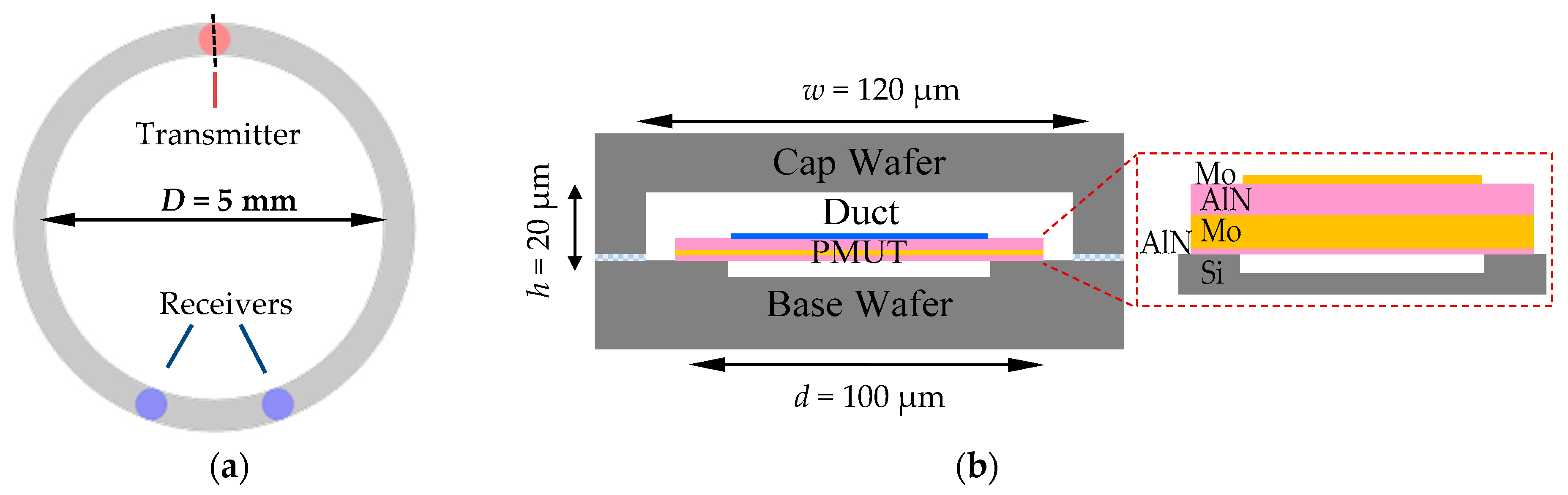
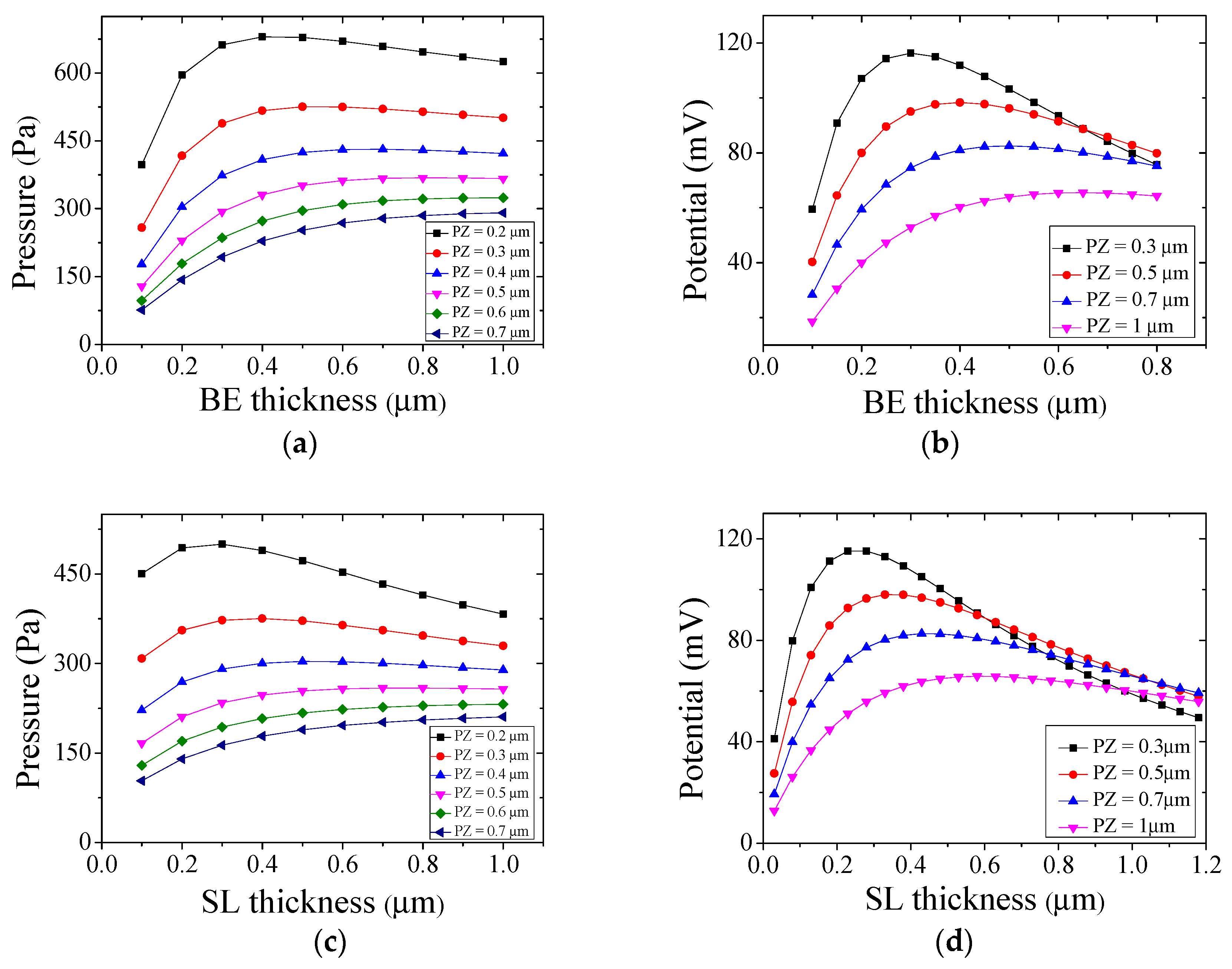
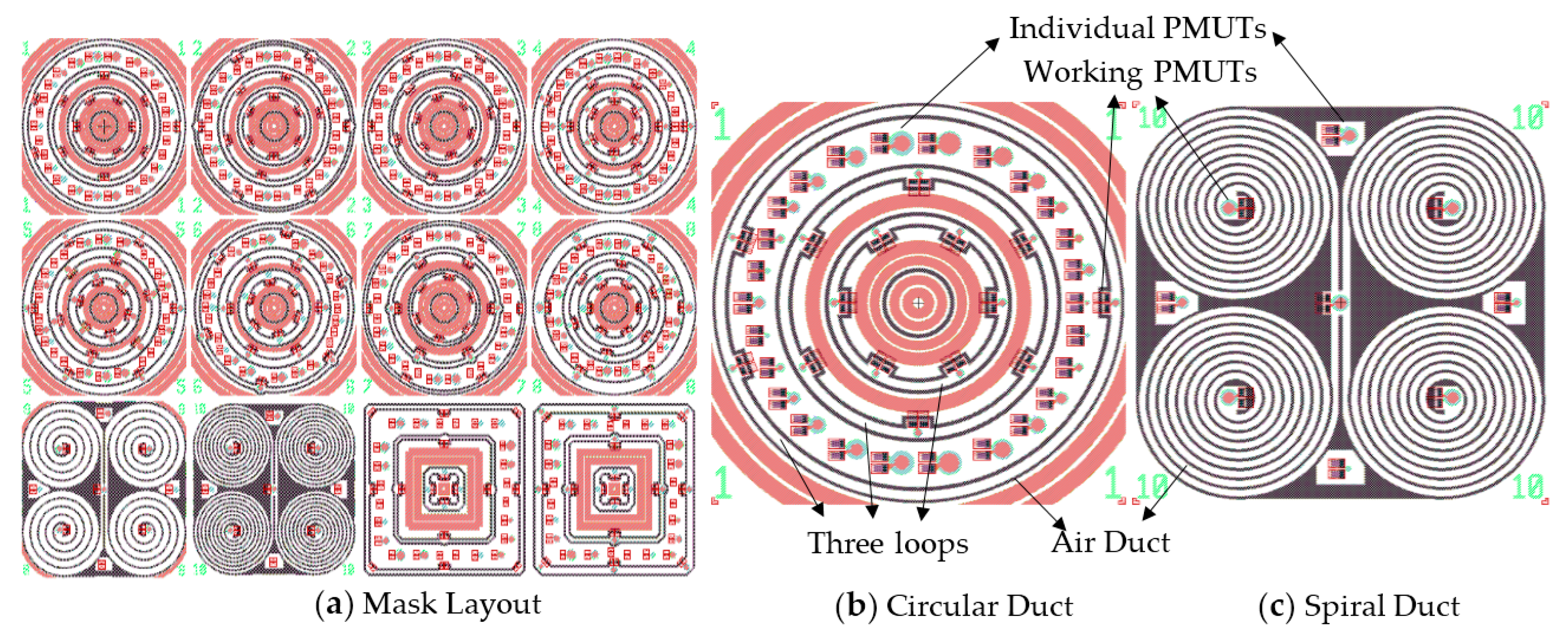
2.2. Design and Structure
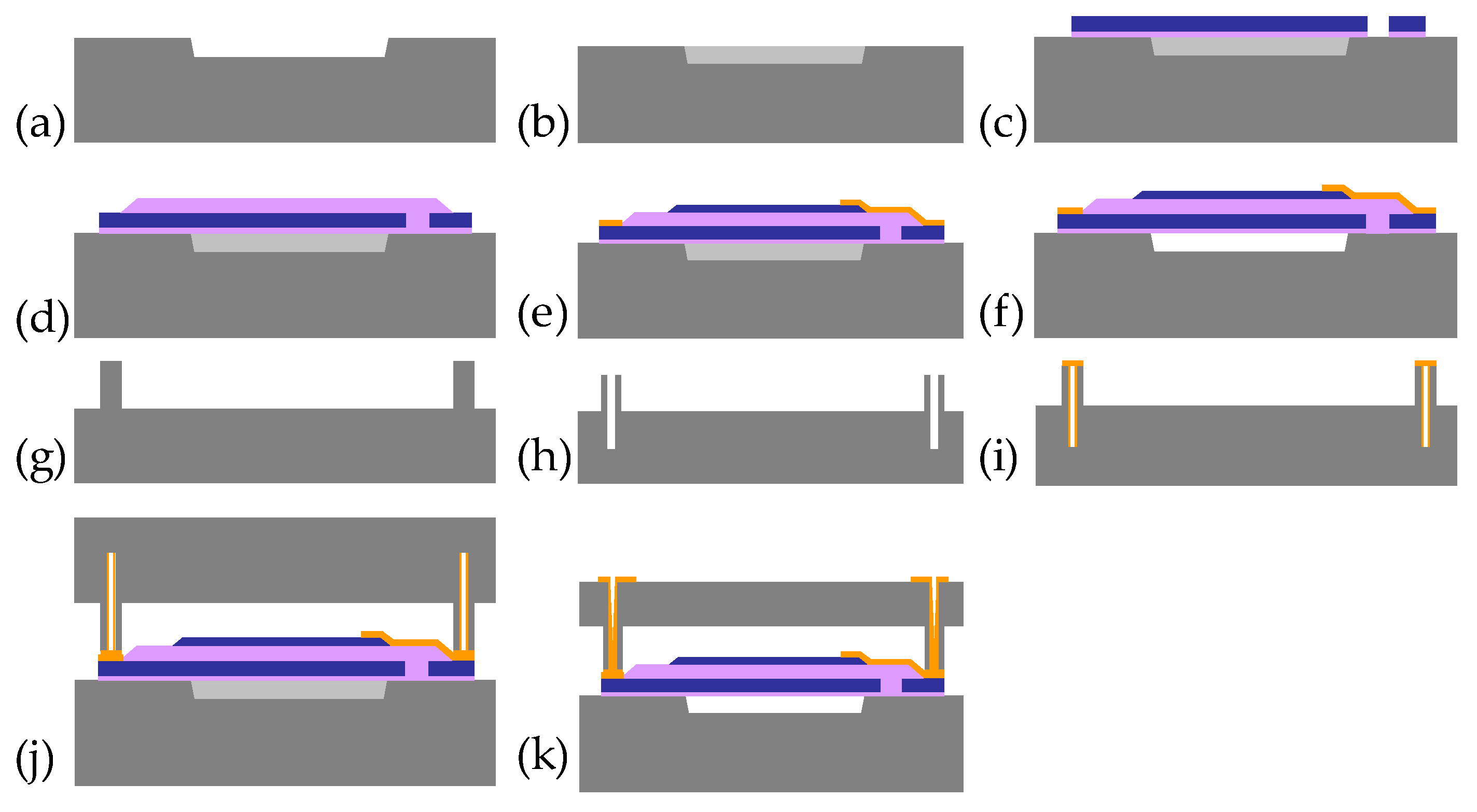
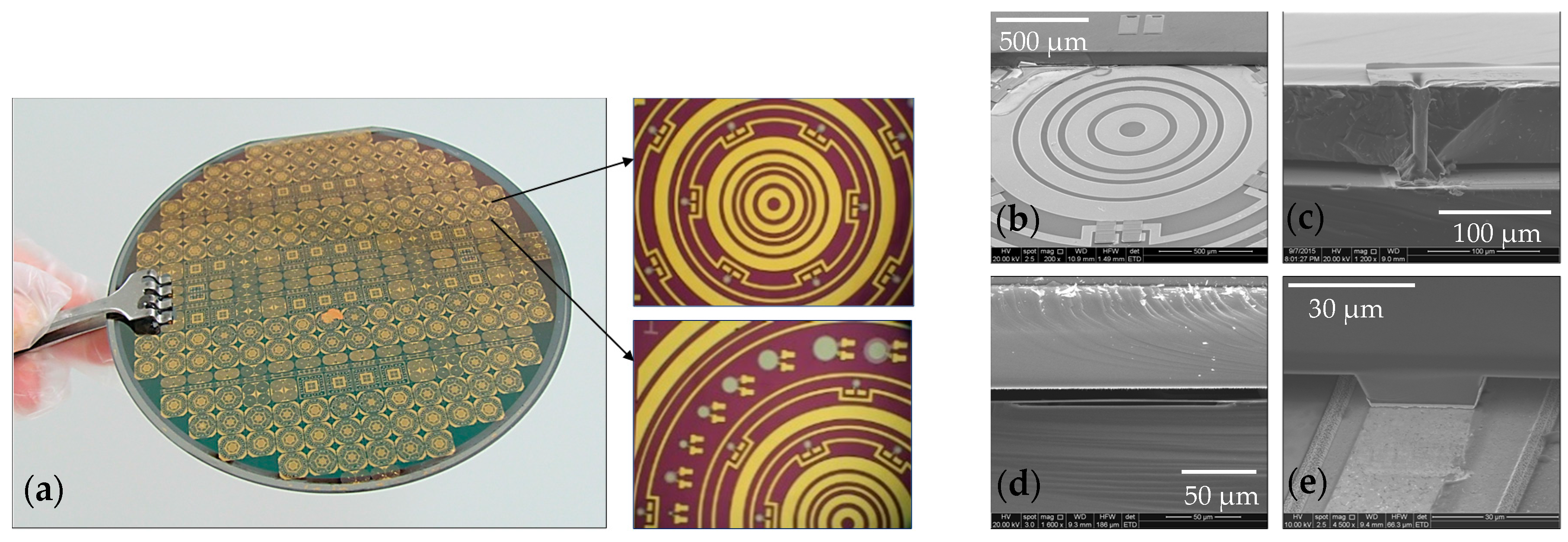
2.3. Fabrication
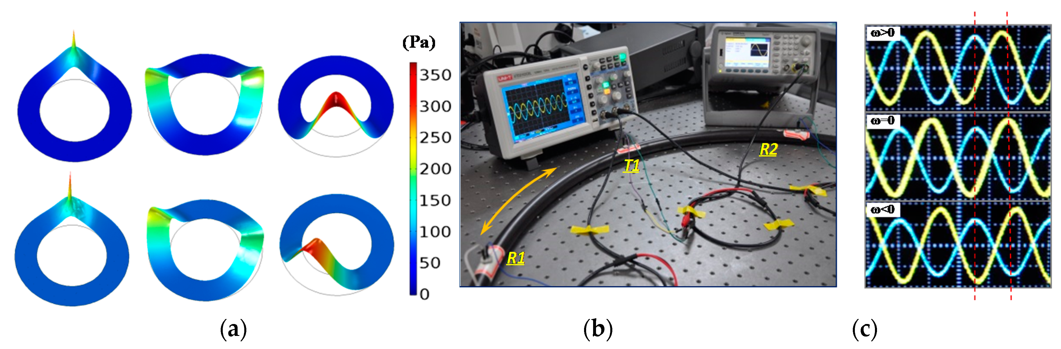
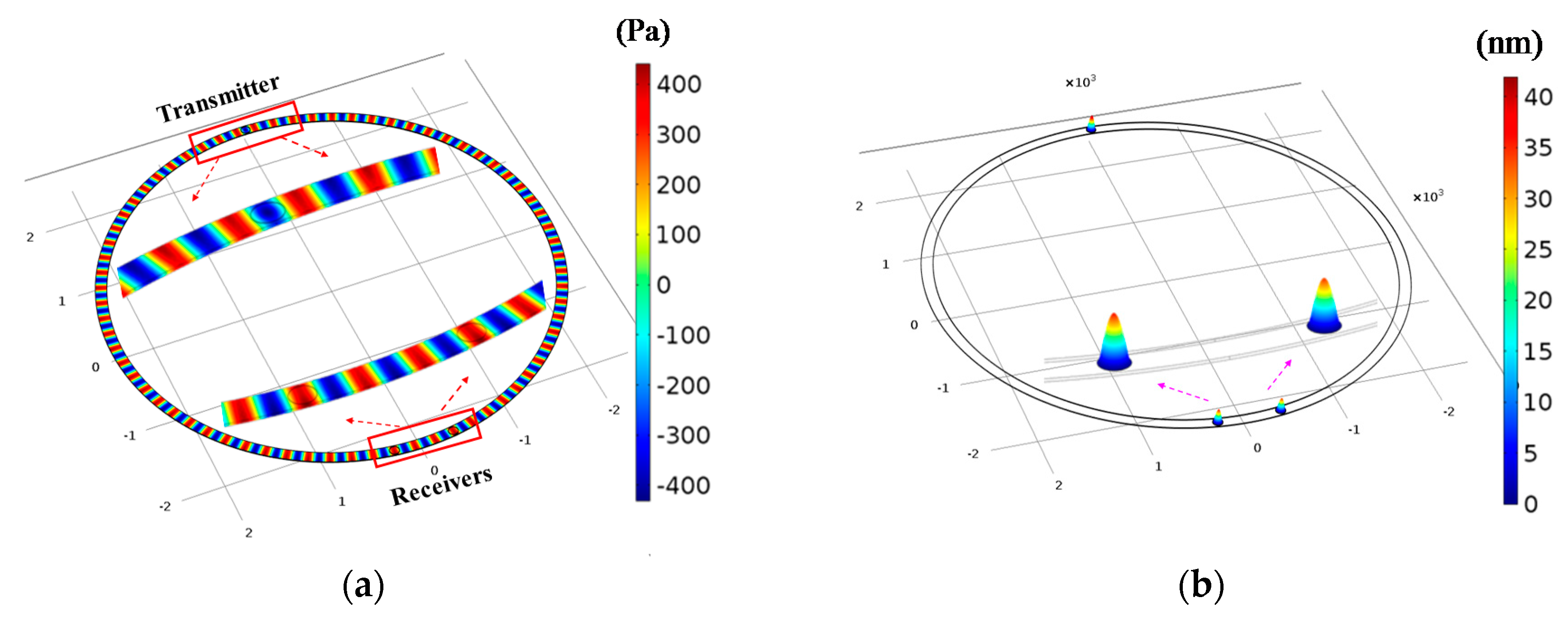
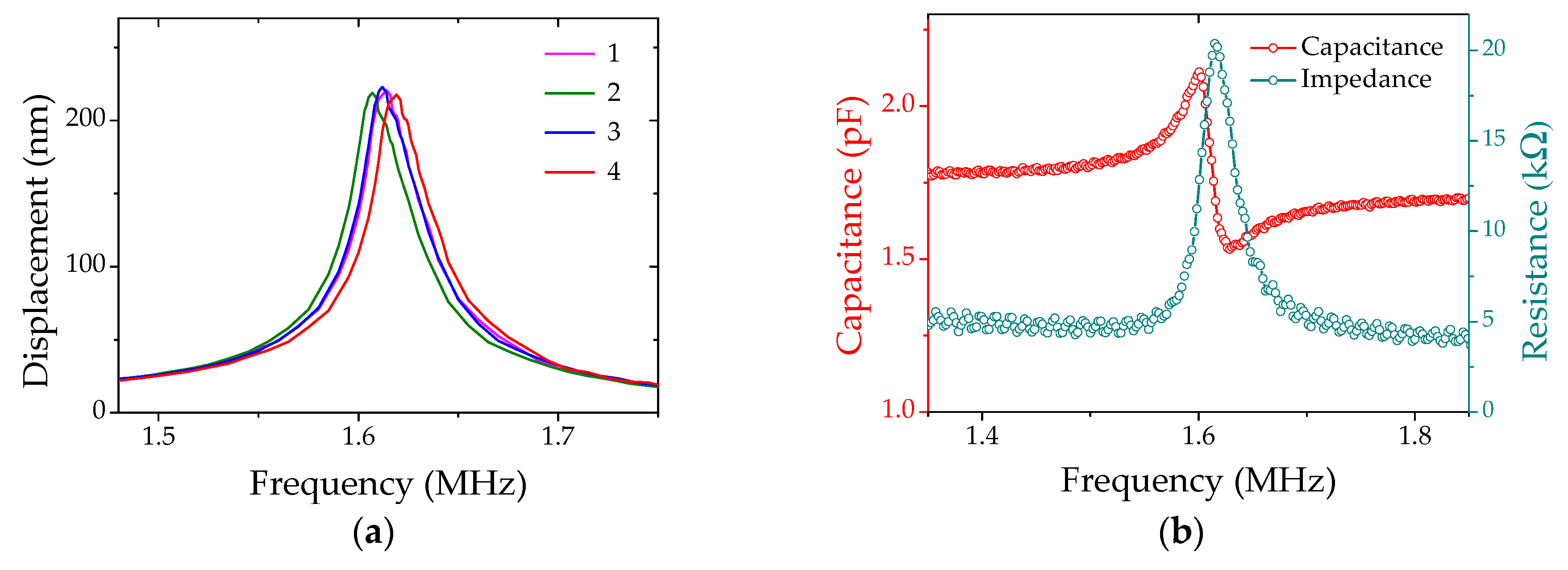
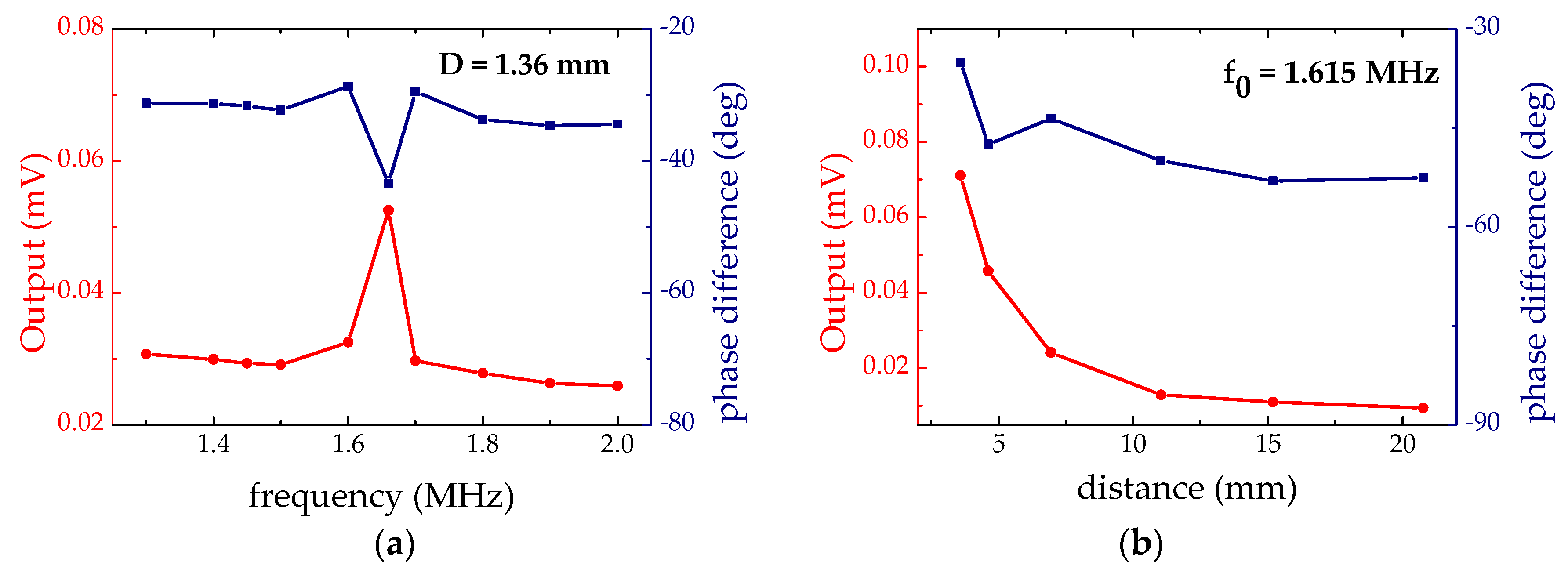
3. Results
4. Conclusions
Acknowledgments
Author Contributions
Conflicts of Interest
References
- Kaajakari, V. Gyroscope. In Practical MEMs; Small Gear Publishing: Las Vegas, NV, USA, 2009; pp. 346–364. [Google Scholar]
- Trusov, A.A.; Schofield, A.R.; Shkel, A.M. Performance characterization of a new temperature-robust gain-bandwidth improved MEMS gyroscope operated in air. Sens. Actuators A Phys. 2009, 155, 16–22. [Google Scholar] [CrossRef]
- Johari, H. Micromachined Capacitive Silicon Bulk Acoustic Wave Gyroscopes. Ph.D. Thesis, Georgia Tech School of Mechanical Engineering, Atlanta, GA, USA, 2008. [Google Scholar]
- Nasiri, S. A Critical Review of MEMS Gyroscopes Technology and Commercialization Status; Invensense: Sunnyvale, CA, USA, 2008; p. 8. [Google Scholar]
- Tronconi, M. MEMS and Sensors Are the Key Enablers of Internet of Things; STMicroelectronics: Geneva, Switzerland, 2013. [Google Scholar]
- Hernandez, J.; Li, Y.; Rehg, J.M.; Picard, R.W. BioGlass: Physiological Parameter Estimation Using a Head-mounted Wearable Device. In Proceedings of the Wireless Mobile Communication and Healthcare, Athens, Greece, 3–5 November 2014; pp. 55–58.
- Pierleoni, P.; Belli, A.; Palma, L.; Pellegrini, M. A High reliability wearable device for elderly fall detection. IEEE Sens. J. 2015, 15, 4544–4553. [Google Scholar] [CrossRef]
- Bernstein, J.; Cho, S.; King, A.T.; Kourepenis, A.; Maciel, P.; Weinberg, M. A micromachined comb-drive tuning fork rate gyroscope. In Proceedings of the IEEE Micro Electro Mechanical Systems, Fort Lauderdale, FL, USA, 10 February 1993; pp. 143–148.
- Yang, C.; Li, H. Digital control system for the MEMS tuning fork gyroscope based on synchronous integral demodulator. IEEE Sens. J. 2015, 15, 5755–5764. [Google Scholar] [CrossRef]
- Varadan, V.K.; Suh, W.D.; Xavier, P.B.; Jose, K.A.; Varadan, V.V. Design and development of a MEMS-IDT gyroscope. Smart Mater. Struct. 2000, 9, 898–905. [Google Scholar]
- Zhang, L.; Masek, V.; Sanatdoost, N.N. Structural optimization of Z-axis tuning-fork MEMS gyroscopes for enhancing reliability and resolution. Microsyst. Technol. 2014, 21, 1187–1201. [Google Scholar] [CrossRef]
- Yazdi, N.; Ayazi, F.; Najafi, K. Micromachined inertial sensors. Proc. IEEE 1998, 86, 1640–1659. [Google Scholar] [CrossRef]
- Faculty, T.A.; Fulfillment, I.P. Degree-Per-Hour Mode-Matched Micromachined Silicon Vibratory Gyroscopes. Ph.D. Thesis, Georgia Tech School of Mechanical Engineering, Atlanta, GA, USA, 2008. [Google Scholar]
- Merlo, S.; Norgia, M.; Donati, S. Fiber gyroscope principles. In Handbook of Fibre Optic Sensing Technology; John Wiley & Sons Ltd.: New York, NY, USA, 2002; pp. 1–23. [Google Scholar]
- Yu, Y.Y.; Chen, B.Y.; Tao, J.; Chen, X.J.; Zhang, H.; Pang, W.; Zhang, D.H.; Luo, H. A novel high sensitivity MEMS acoustic gyroscope by measuring phase shift. In Proceedings of the IEEE Sensors, Busan, Korea, 1–4 November 2015.
- Sanders, G.A.; Sanders, S.J.; Strandjord, L.K.; Qiu, T.; Wu, J.; Smiciklas, M.; Salit, M. Fiber optic gyroscope development at Honeywell. In Proceedings of the SPIE Commercial+ Scientific Sensing and Imaging, International Society for Optics and Photonics, Baltimore, MD, USA, 14 May 2016.
- Song, N.; Cai, W.; Song, J.; Jin, J.; Wu, C. Structure optimization of small-diameter polarization-maintaining photonic crystal fiber for mini coil of space borne miniature fiber-optic gyroscope. Appl. Opt. 2015, 54, 9831–9838. [Google Scholar] [CrossRef] [PubMed]
- Ciminelli, C.; Dell’Olio, F.; Armenise, M.N. High-Q spiral resonator for optical gyroscope applications: numerical and experimental investigation. IEEE Photonics J. 2012, 4, 1844–1854. [Google Scholar] [CrossRef]
- Lu, Y.; Shelton, S.; Horsley, D.A. High frequency and high fill factor piezoelectric micromachined ultrasonic transducers based on cavity SOI wafers. In Proceedings of the Solid-State Sensors, Actuators, and Microsystems Workshop, Hilton Head Island, SC, USA, 8–12 June 2014; pp. 131–134.
- Lu, Y.; Heidari, A.; Horsley, D.A. A high fill-factor annular array of high frequency piezoelectric micromachined ultrasonic transducers. J. Microelectromech. Syst. 2015, 24, 904–913. [Google Scholar] [CrossRef]
- Przybyla, R.; Izyumin, I.; Kline, M.; Boser, B.; Shelton, S. An ultrasonic rangefinder based on an AlN piezoelectric micromachined ultrasound transducer. In Proceedings of the IEEE Sensors, Waikoloa, HI, USA, 1–4 November 2010; pp. 2417–2421.
- Wygant, I.O.; Kupnik, M.J.; Windsor, J.C.; Wright, W.M.; Wochner, M.S.; Hamilton, M.F. 50 kHz capacitive micromachined ultrasonic transducers for generation of highly directional sound with parametric arrays. IEEE Trans. Ultrason. Ferroelectr. Freq. Control 2009, 56, 193–203. [Google Scholar] [CrossRef] [PubMed]
- Shelton, S.; Chan, M.L.; Park, H.; Horsley, D.A. CMOS-compatible AlN piezoelectric micromachined ultrasonic transducers. In Proceedings of the IEEE International Ultrasonics Symposium, Rome, Italy, 20–23 September 2009; pp. 402–405.
- Lu, Y.; Heidari, A.; Shelton, S.; Guedes, A.; Horsley, D.A. High frequency piezoelectric micromachined ultrasonic transducer array for intravascular ultrasound imaging. In Proceedings of the IEEE 27th MEMS, San Francisco, CA, USA, 26–30 January 2014; pp. 745–748.
- Muralt, P.; Ledermann, N.; Paborowski, J.; Barzegar, A.; Gentil, S.; Belgacem, B.; Petitgrand, S.; Bosseboeuf, A.; Setter, N. Piezoelectric micromachined ultrasonic transducers based on PZT thin films. IEEE Trans. Ultrason. Ferroelectr. Freq. Control 2005, 52, 2276–2288. [Google Scholar] [CrossRef] [PubMed]
- Shelton, S.; Rozen, O.; Guedes, A.; Przybyla, R.; Boser, B.; Horsley, D.A. Improved acoustic coupling of air-coupled micromachined ultrasonic transducers. In Proceedings of the 2014 IEEE 27th International Conference on Micro Electro Mechanical Systems, San Francisco, CA, USA, 26–30 January 2014; pp. 753–756.
- Sammoura, F.; Smyth, K.; Kim, S.-G. Optimizing the electrode size of circular bimorph plates with different boundary conditions for maximum deflection of piezoelectric micromachined ultrasonic transducers. Ultrasonics 2013, 53, 328–334. [Google Scholar] [CrossRef] [PubMed]
- Lu, Y.; Horsley, D.A. Modeling, fabrication, and characterization of piezoelectric micromachined ultrasonic transducer arrays based on cavity SOI wafers. J. Microelectromech. Syst. 2015, 24, 1142–1149. [Google Scholar] [CrossRef]
- Horsley, D.A.; Rozen, O.; Lu, Y.; Shelton, S.; Guedes, A.; Przybyla, R.; Tang, H.Y.; Boser, B.E. Piezoelectric micromachined ultrasonic transducers for human-machine interfaces and biometric sensing. In Proceedings of the IEEE Sensors, Melbourne, Australia, 2–5 November 2015.
- Muralt, P.; Baborowski, J. Micromachined ultrasonic transducers and acoustic sensors based on piezoelectric thin films. J. Electroceram. 2004, 12, 101–108. [Google Scholar] [CrossRef]
- Li, X.; Xu, L.; Sun, T. Piezoelectric micromachined ultrasonic transducer array for micro audio directional loudspeaker. In Proceedings of the IEEE International Conference on Mechatronics and Automation, Takamatsu, Japan, 4–7 August 2013; pp. 450–455.
- Qiu, Y.Q.; Gigliotti, J.V.; Wallace, M.; Griggio, F.; Demore, C.E.M.; Cochran, S.; McKinstry, T.S. Piezoelectric micromachined ultrasound transducer (PMUT) arrays for integrated sensing, actuation and imaging. Sensors 2015, 15, 8020–8041. [Google Scholar] [CrossRef] [PubMed]
- Przybyla, R.; Flynn, A.; Jain, V.; Shelton, S.; Guedes, A.A.; Izyumin, I.; Horsley, D.; Boser, B.E. A micromechanical ultrasonic distance sensor with > 1 meter range. In Proceedings of the 16th International Solid-State Sensors, Actuators and Microsystems Conference (TRANSDUCERS), Beijing, China, 5–9 June 2011; pp. 2070–2073.
- Shelton, S.; Guedes, A.; Przybyla, R.; Tsai, J.M. Aluminum nitride piezoelectric micromachined ultrasound transducer arrays. In Proceedings of the Solid-State Sensors, Actuators, and Microsystems Workshop, Hilton Head, SC, USA, 11–14 June 2012; pp. 291–294.
- Kinsler, L.E.; Fery, A.R.; Coppens, A.B.; Sanders, J.V. Fundamentals of Acoustics; Wiley: Hoboken, NJ, USA, 1999. [Google Scholar]
- Blackstock, D. Fundamentals of Physical Acoustics; John Wiley & Sons: Hoboken, NJ, USA, 2000. [Google Scholar]
- Tang, H.; Hu, Y.; Fung, S.; Tsai, J.M. Pulse-echo ultrasonic fingerprint sensor on a chip. In Proceedings of the 18th Solid-State Sensors, Actuators and Microsystems (TRANSDUCERS), Anchorage, AK, USA, 21–25 June 2015; pp. 674–677.
- ANSI/IEEE Std 176-1987, IEEE Standard on Piezoelectricity; The Institute of Electrical and Electronics Engineers, Inc.: New York, NY, USA, 1988.
- Sammoura, F.; Shelton, S.; Akhbari, S.; Horsley, D.; Lin, L.L. A Two-Port Piezoelectric Micromachined Ultrasonic Transducer. In Proceedings of the 2014 Joint IEEE International Symposium on the Applications of Ferroelectrics, International Workshop on Acoustic Transduction Materials and Devices & Workshop on Piezoresponse Force Microscopy (ISAF/IWATMD/PFM), State College, PA, USA, 1–4 May 2014.
- Geng, Y.L.; Xu, L.M.; Wang, Y. Optimization of a circular piezoelectric micro-mechanical ultrasonic transducer on electromechanical coupling coefficient. In Proceedings of the Piezoelectricity, Acoustic Waves, and Device Applications (SPAWDA) and 2009 China Symposium on Frequency Control Technology, Wuhan, China, 17–20 December 2009.
- Jung, J.; Kim, S.; Lee, W.; Choi, H. Fabrication of a two-dimensional piezoelectric micromachined ultrasonic transducer array using a top-crossover-to-bottom structure and metal bridge connections. J. Micromech. Microeng. 2013, 23, 125037. [Google Scholar] [CrossRef]


© 2016 by the authors. Licensee MDPI, Basel, Switzerland. This article is an open access article distributed under the terms and conditions of the Creative Commons Attribution (CC-BY) license ( http://creativecommons.org/licenses/by/4.0/).
Share and Cite
Yu, Y.; Luo, H.; Chen, B.; Tao, J.; Feng, Z.; Zhang, H.; Guo, W.; Zhang, D. MEMS Gyroscopes Based on Acoustic Sagnac Effect. Micromachines 2017, 8, 2. https://doi.org/10.3390/mi8010002
Yu Y, Luo H, Chen B, Tao J, Feng Z, Zhang H, Guo W, Zhang D. MEMS Gyroscopes Based on Acoustic Sagnac Effect. Micromachines. 2017; 8(1):2. https://doi.org/10.3390/mi8010002
Chicago/Turabian StyleYu, Yuanyuan, Hao Luo, Buyun Chen, Jin Tao, Zhihong Feng, Hao Zhang, Wenlan Guo, and Daihua Zhang. 2017. "MEMS Gyroscopes Based on Acoustic Sagnac Effect" Micromachines 8, no. 1: 2. https://doi.org/10.3390/mi8010002