

Fast Fitting of the Dynamic Memdiode Model to the Conduction Characteristics of RRAM Devices Using Convolutional Neural Networks
 , , , , and
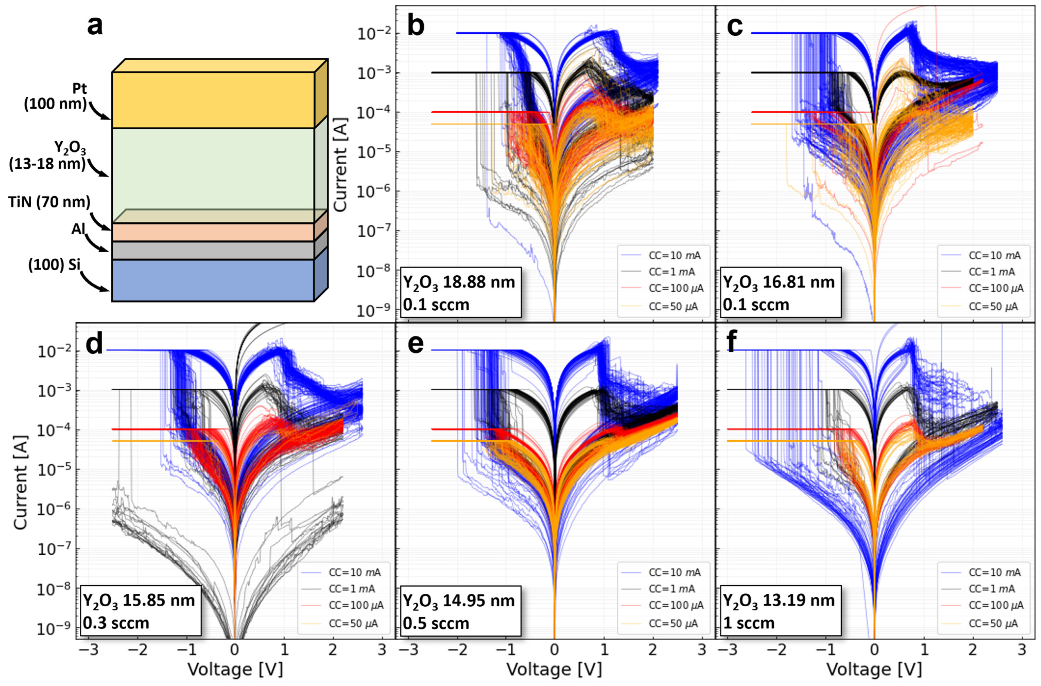
Abstract
:1. Introduction
2. Materials and Methods
2.1. Device Fabrication and Electrical Characterization
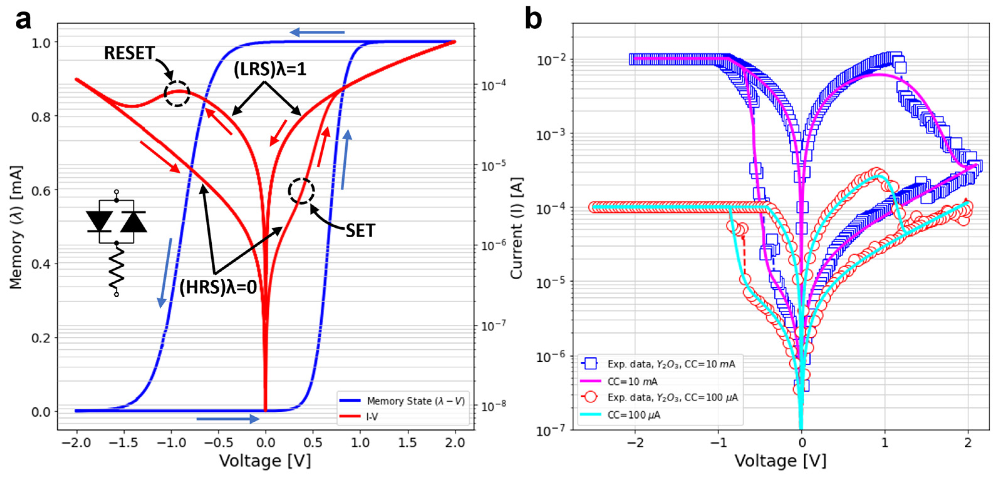
2.2. Dynamic Memdiode Model (DMM)
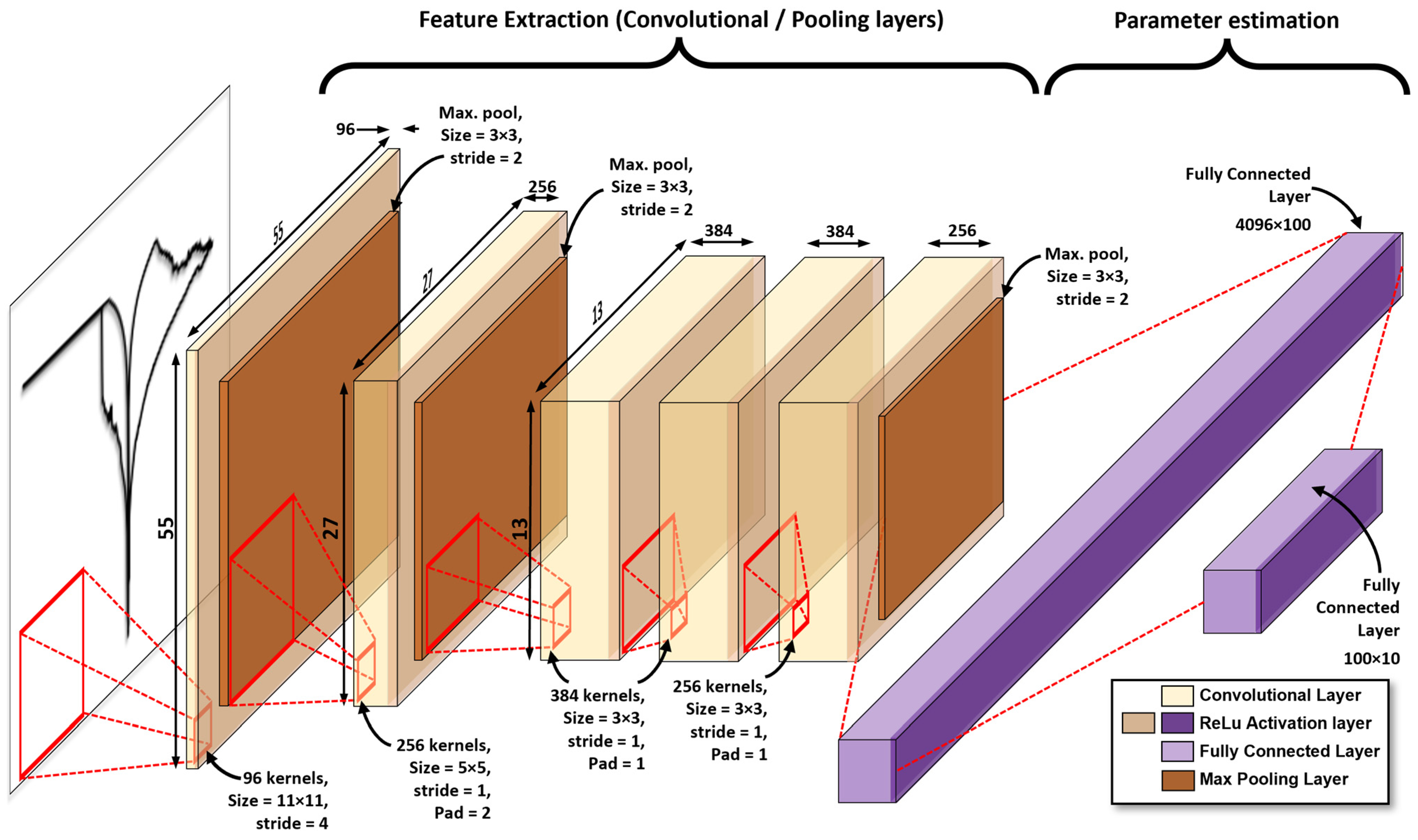
2.3. Convolutional Neural Networks (CNNs)
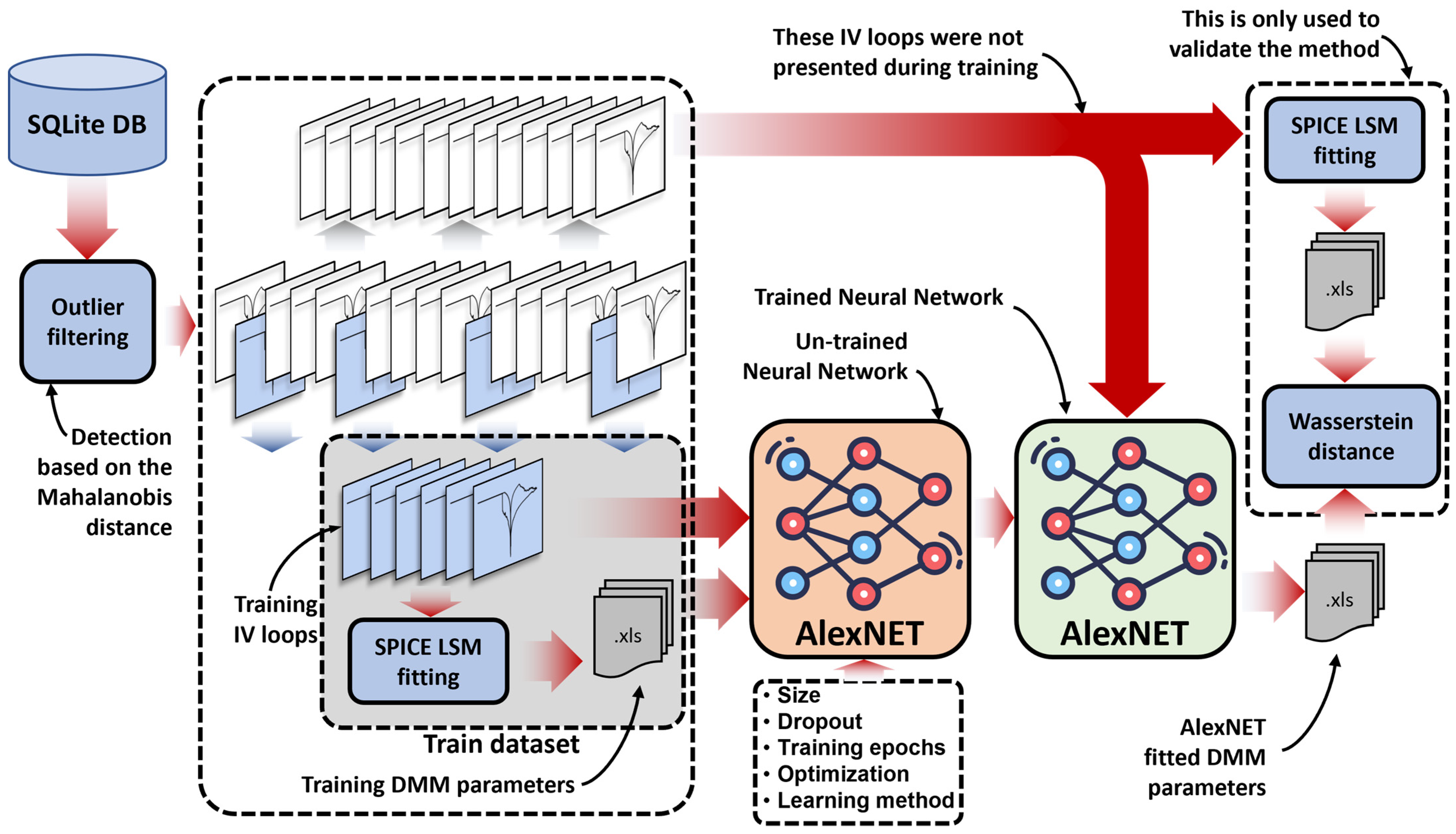
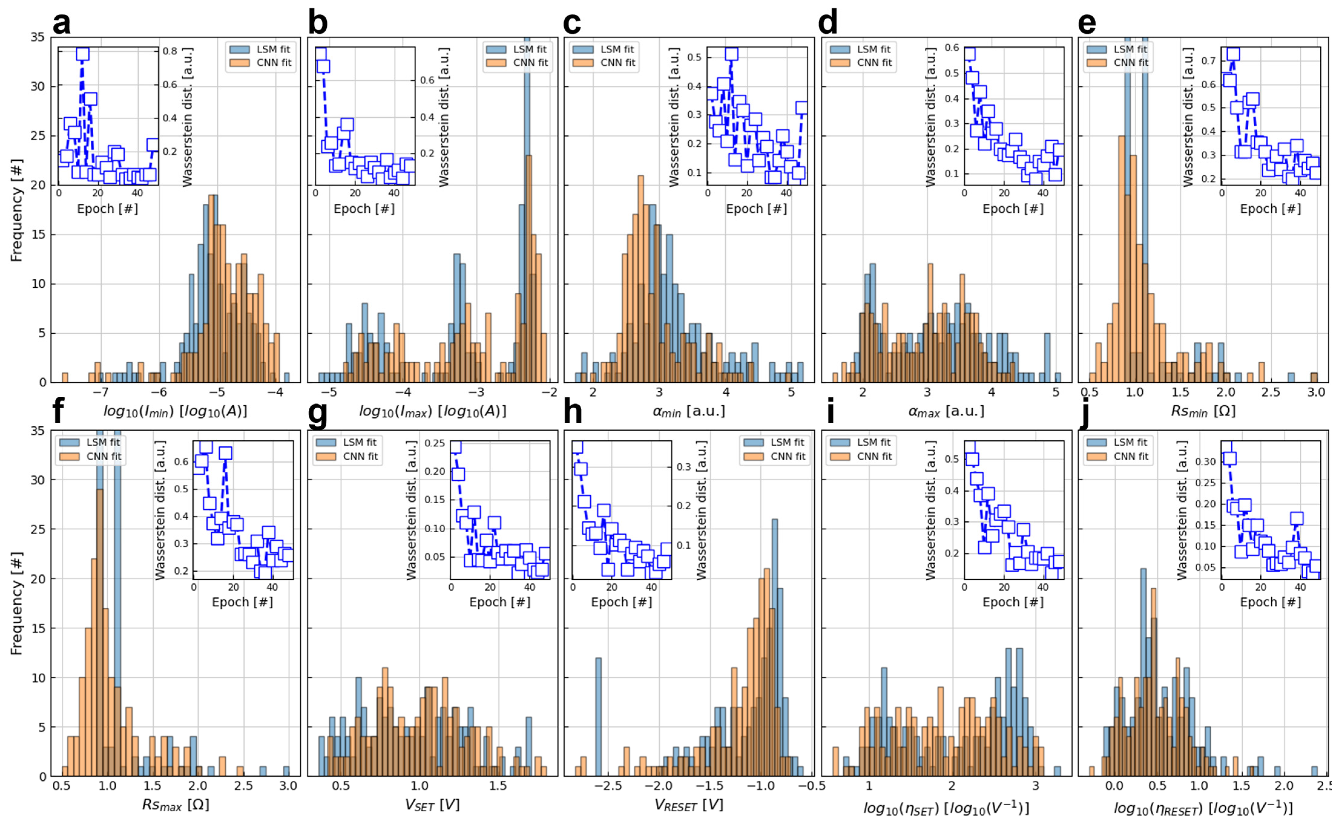
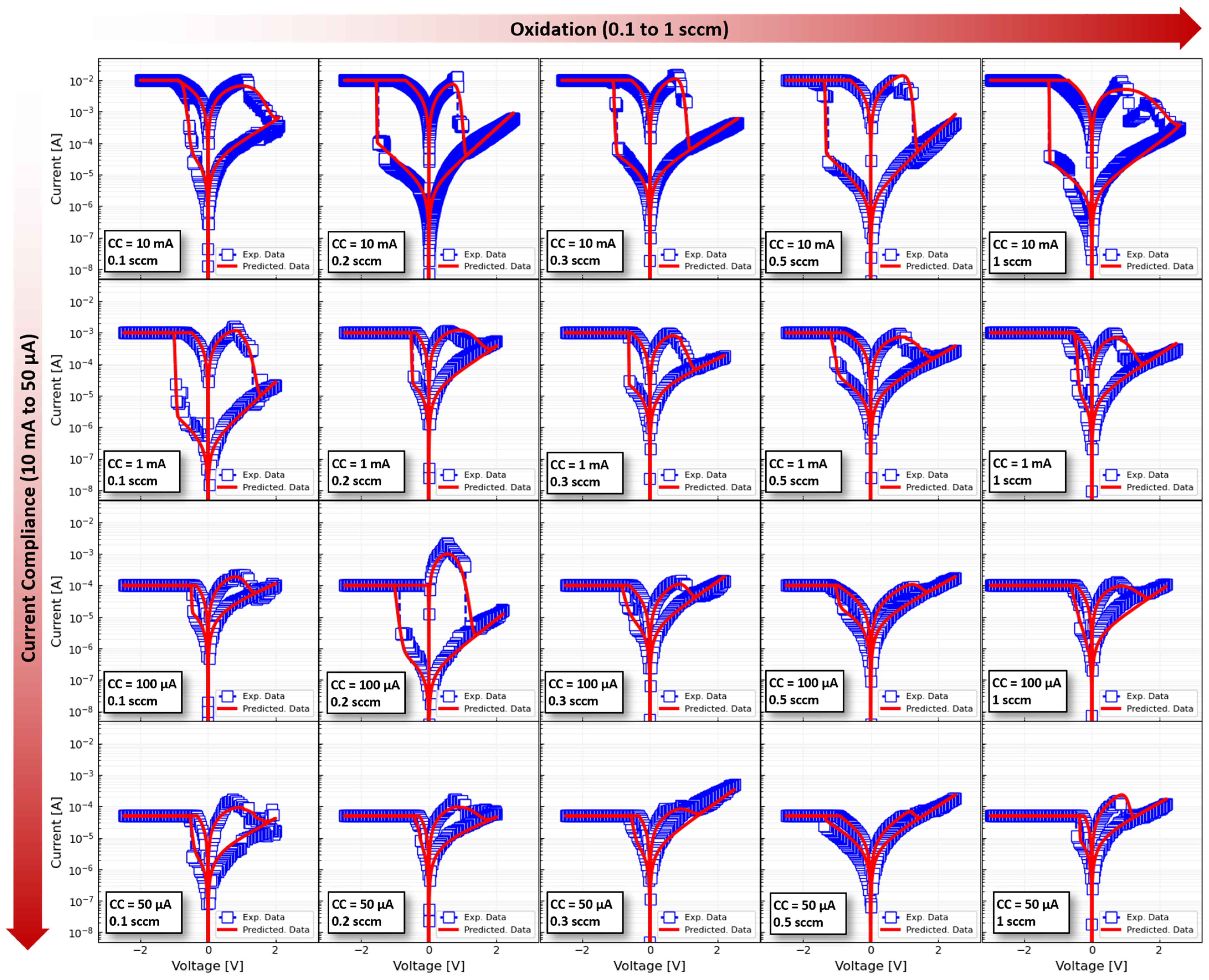
2.4. Database Generation
- (i)
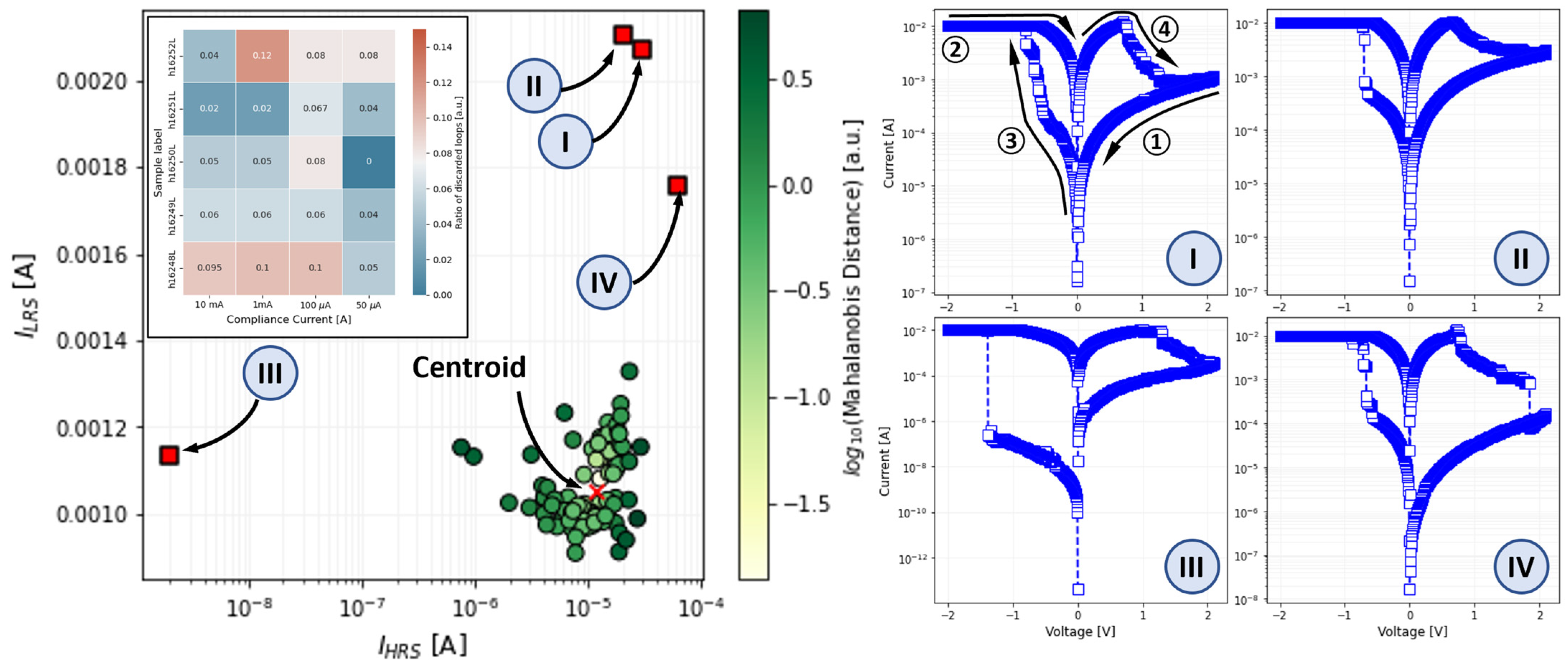
- The I-V loop data is divided into 4 segments: HRS region (from the maximal voltage during the RESET Vmax→0, ① in Figure 1c), LRS region (from the minimal volage applied during SET, Vmin→0, ②), SET region (from 0→Vmax, ③), and RESET region (from 0→Vmin, ④).
- (ii)
- Each previously mentioned segment is fitted using an approximation of the DMM mathematically derived for the region of interest (and thus neglecting or keeping constant the parameters associated with out-of-scope regions).
- (iii)
- Considering the previous fitting as an initial guess, the optimum parameter values are found by numerical optimization, consisting in an iterative simulation with the SPICE version of the DMM model.
- (iv)
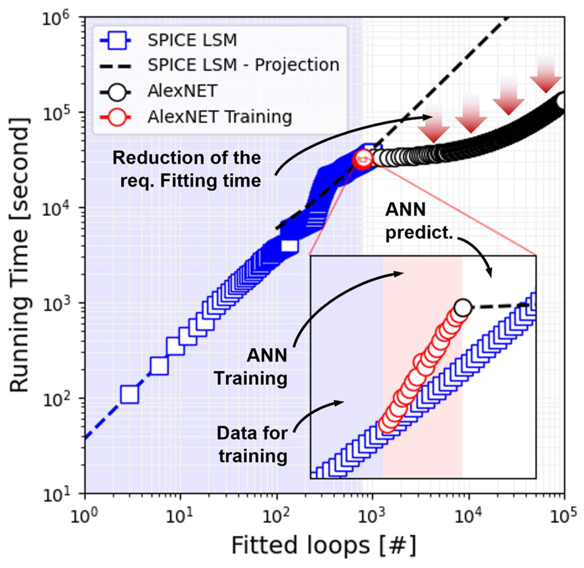
- For performance comparisons, which are described later in the paper, the time required to fit each loop was recorded.
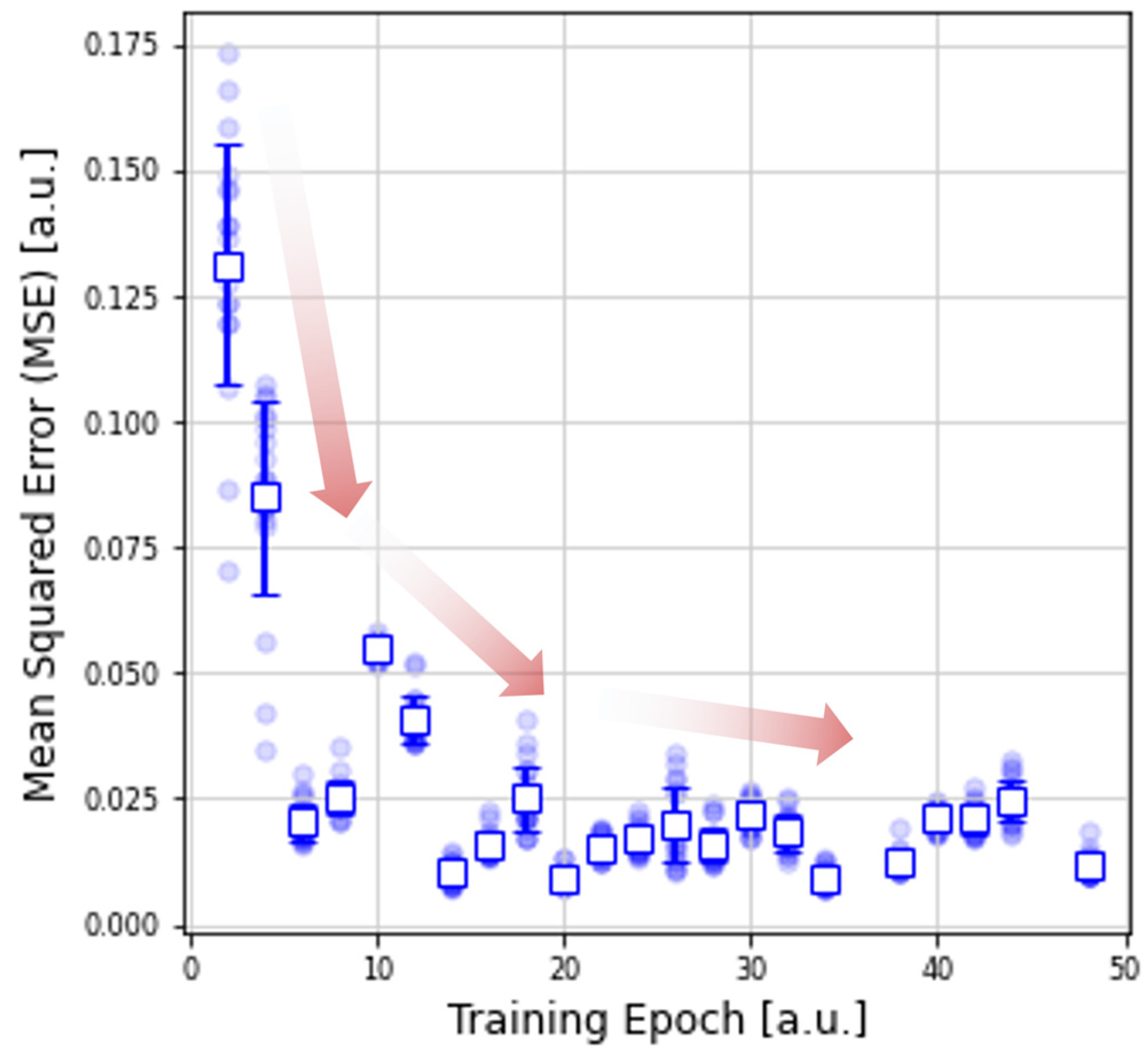
2.5. ANN-Based DMM Fitting Procedure
3. Results and Discussion
4. Conclusions
Author Contributions
Funding
Conflicts of Interest
References
- Strukov, D.B.; Snider, G.S.; Stewart, D.R.; Williams, R.S. The missing memristor found. Nature 2008, 453, 80–83. [Google Scholar] [CrossRef] [PubMed]
- Miranda, E. Compact Model for the Major and Minor Hysteretic I-V Loops in Nonlinear Memristive Devices. IEEE Trans. Nanotechnol. 2015, 14, 787–789. [Google Scholar] [CrossRef]
- Aguirre, F.L.; Pazos, S.M.; Palumbo, F.; Suñé, J.; Miranda, E. Application of the Quasi-Static Memdiode Model in Cross-Point Arrays for Large Dataset Pattern Recognition. IEEE Access 2020, 8, 202174–202193. [Google Scholar] [CrossRef]
- Aguirre, F.L.; Gomez, N.M.; Pazos, S.M.; Palumbo, F.; Suñé, J.; Miranda, E. Minimization of the Line Resistance Impact on Memdiode-Based Simulations of Multilayer Perceptron Arrays Applied to Pattern Recognition. J. Low Power Electron. Appl. 2021, 11, 9. [Google Scholar] [CrossRef]
- Levenberg, K. A Method for the Solution of Certain Non-Linear Problems in Least Squares. Q. Appl. Math. 1944, 2, 164–168. [Google Scholar] [CrossRef] [Green Version]
- Marquardt, D.W. An Algorithm for Least-Squares Estimation of Nonlinear Parameters. J. Soc. Ind. Appl. Math. 1963, 11, 431–441. [Google Scholar] [CrossRef]
- Singh, K.; Jain, P. BSIM3v3 to EKV2.6 Model Parameter Extraction and Optimisation using LM Algorithm on 0.18 µ Technology node. Int. J. Electron. Telecommun. 2018, 64, 5–11. [Google Scholar] [CrossRef]
- Karr, C.L.; Weck, B.; Massart, D.L.; Vankeerberghen, P. Least median squares curve fitting using a genetic algorithm. Eng. Appl. Artif. Intell. 1995, 8, 177–189. [Google Scholar] [CrossRef]
- Fogel, D.B. Evolutionary Computation: The Fossil Record; IEEE Press: New York, NY, USA, 1998; ISBN 9780780334816. [Google Scholar]
- Jervase, J.A.; Bourdoucen, H.; Al-Lawati, A. Solar cell parameter extraction using genetic algorithms. Meas. Sci. Technol. 2001, 12, 1922–1925. [Google Scholar] [CrossRef] [Green Version]
- Spałek, T.; Pietrzyk, P.; Sojka, Z. Application of the genetic algorithm joint with the Powell method to nonlinear least-squares fitting of powder EPR spectra. J. Chem. Inf. Model. 2005, 45, 18–29. [Google Scholar] [CrossRef]
- Hooke, R.; Jeeves, T.A. “Direct Search” Solution of Numerical and Statistical Problems. J. ACM 1961, 8, 212–229. [Google Scholar] [CrossRef]
- Torczon, V. On the Convergence of Pattern Search Algorithms. SIAM J. Optim. 1997, 7, 1–25. Available online: http://www.siam.org/journals/ojsa.php (accessed on 25 September 2022). [CrossRef]
- Ayala-Mató, F.; Seuret-Jiménez, D.; Escobedo-Alatorre, J.J.; Vigil-Galán, O.; Courel, M. A hybrid method for solar cell parameter estimation. J. Renew. Sustain. Energy 2017, 9, 063504. [Google Scholar] [CrossRef]
- Bishop, C.M.; Roach, C.M. Fast curve fitting using neural networks. Rev. Sci. Instrum. 1992, 63, 4450–4456. [Google Scholar] [CrossRef] [Green Version]
- Krizhevsky, A.; Sutskever, I.; Hinton, G.E. ImageNet classification with deep convolutional neural networks. Commun. ACM 2017, 60, 84–90. [Google Scholar] [CrossRef] [Green Version]
- Sharath, S.U.; Vogel, S.; Molina-Luna, L.; Hildebrandt, E.; Wenger, C.; Kurian, J.; Duerrschnabel, M.; Niermann, T.; Niu, G.; Calka, P.; et al. Control of Switching Modes and Conductance Quantization in Oxygen Engineered HfOx based Memristive Devices. Adv. Funct. Mater. 2017, 27, 1700432. [Google Scholar] [CrossRef]
- Petzold, S.; Piros, E.; Eilhardt, R.; Zintler, A.; Vogel, T.; Kaiser, N.; Radetinac, A.; Komissinskiy, P.; Jalaguier, E.; Nolot, E.; et al. Tailoring the Switching Dynamics in Yttrium Oxide-Based RRAM Devices by Oxygen Engineering: From Digital to Multi-Level Quantization toward Analog Switching. Adv. Electron. Mater. 2020, 6, 2000439. [Google Scholar] [CrossRef]
- Lee, A.R.; Bae, Y.C.; Im, H.S.; Hong, J.P. Complementary resistive switching mechanism in Ti-based triple TiO x /TiN/TiO x and TiOx/TiOxNy/TiOx matrix. Appl. Surf. Sci. 2013, 274, 85–88. [Google Scholar] [CrossRef]
- Duan, W.J.; Wang, J.B.; Zhong, X.L.; Song, H.J.; Li, B. Complementary resistive switching in single sandwich structure for crossbar memory arrays. J. Appl. Phys. 2016, 120, 084502. [Google Scholar] [CrossRef]
- Yang, M.; Wang, H.; Ma, X.; Gao, H.; Hao, Y. Voltage-amplitude-controlled complementary and self-compliance bipolar resistive switching of slender filaments in Pt/HfO2/HfOx/Pt memory devices. J. Vac. Sci. Technol. B Nanotechnol. Microelectron. Mater. Process. Meas. Phenom. 2017, 35, 032203. [Google Scholar] [CrossRef]
- Chen, C.; Gao, S.; Tang, G.; Fu, H.; Wang, G.; Song, C.; Zeng, F.; Pan, F. Effect of electrode materials on AlN-based bipolar and complementary resistive switching. ACS Appl. Mater. Interfaces 2013, 5, 1793–1799. [Google Scholar] [CrossRef] [PubMed]
- Aguirre, F.L.; Rodriguez-Fernandez, A.; Pazos, S.M.; Sune, J.; Miranda, E.; Palumbo, F. Study on the Connection Between the Set Transient in RRAMs and the Progressive Breakdown of Thin Oxides. IEEE Trans. Electron Devices 2019, 66, 3349–3355. [Google Scholar] [CrossRef] [Green Version]
- Fröhlich, K.; Kundrata, I.; Blaho, M.; Precner, M.; Tapajna, M.; Klimo, M.; Šuch, O.; Škvarek, O. Hafnium oxide and tantalum oxide based resistive switching structures for realization of minimum and maximum functions. J. Appl. Phys. 2018, 124, 152109. [Google Scholar] [CrossRef]
- Sune, J.; Miranda, E.; Nafria, M.; Aymerich, X. Point contact conduction at the oxide breakdown of MOS devices. In Proceedings of the IEEE Technical Digest—IEDM, San Francisco, CA, USA, 6–9 December 1998; pp. 191–194. [Google Scholar]
- Miranda, E.; Suñé, J. Analytic modeling of leakage current through multiple breakdown paths in SiO2 films. In Proceedings of the IEEE International Reliability Physics Symposium Proceedings, Orlando, FL, USA, 30 April–3 May 2001; Institute of Electrical and Electronics Engineers Inc.: New York, NY, USA, 2001; Volume 2001, pp. 367–379. [Google Scholar]
- Miranda, E.; Suñé, J. Electron transport through broken down ultra-thin SiO2 layers in MOS devices. Microelectron. Reliab. 2004, 44, 1–23. [Google Scholar] [CrossRef]
- Miranda, E.; Walczyk, C.; Wenger, C.; Schroeder, T. Model for the Resistive Switching Effect in HfO2 MIM Structures Based on the Transmission Properties of Narrow Constrictions. IEEE Electron Device Lett. 2010, 31, 609–611. [Google Scholar] [CrossRef]
- Datta, S. Electronic Transport in Mesoscopic Systems, 1st ed.; Cambridge Studies in Semiconductor Physics and Microelectronic Engineering; Cambridge University Press: Cambridge, UK, 1997; ISBN 978-0521599436. [Google Scholar]
- Miranda, E.; Mehonic, A.; Suñé, J.; Kenyon, A.J. Multi-channel conduction in redox-based resistive switch modelled using quantum point contact theory. Appl. Phys. Lett. 2013, 103, 222904. [Google Scholar] [CrossRef] [Green Version]
- Miranda, E.; Sune, J. Memristive State Equation for Bipolar Resistive Switching Devices Based on a Dynamic Balance Model and Its Equivalent Circuit Representation. IEEE Trans. Nanotechnol. 2020, 19, 837–840. [Google Scholar] [CrossRef]
- Rodriguez-Fernandez, A.; Cagli, C.; Sune, J.; Miranda, E. Switching Voltage and Time Statistics of Filamentary Conductive Paths in HfO2-based ReRAM Devices. IEEE Electron Device Lett. 2018, 39, 656–659. [Google Scholar] [CrossRef] [Green Version]
- Aguirre, F.L.; Suñé, J.; Miranda, E. SPICE Implementation of the Dynamic Memdiode Model for Bipolar Resistive Switching Devices. Micromachines 2022, 13, 330. [Google Scholar] [CrossRef]
- Dua, V. An Artificial Neural Network approximation based decomposition approach for parameter estimation of system of ordinary differential equations. Comput. Chem. Eng. 2011, 35, 545–553. [Google Scholar] [CrossRef]
- Parikh, J.; Kozloski, J.; Gurev, V. Integration of AI and mechanistic modeling in generative adversarial networks for stochastic inverse problems. arXiv 2020, arXiv:2009.08267. [Google Scholar]
- Gonçalves, P.J.; Lueckmann, J.M.; Deistler, M.; Nonnenmacher, M.; Öcal, K.; Bassetto, G.; Chintaluri, C.; Podlaski, W.F.; Haddad, S.A.; Vogels, T.P.; et al. Training deep neural density estimators to identify mechanistic models of neural dynamics. Elife 2020, 9, 1–46. [Google Scholar] [CrossRef] [PubMed]
- Rudi, J.; Bessac, J.; Lenzi, A. Parameter Estimation with Dense and Convolutional Neural Networks Applied to the FitzHugh-Nagumo ODE. arXiv 2021, arXiv:2012.06691. [Google Scholar]
- Abdel-Hamid, O.; Mohamed, A.R.; Jiang, H.; Deng, L.; Penn, G.; Yu, D. Convolutional neural networks for speech recognition. IEEE Trans. Audio Speech Lang. Process. 2014, 22, 1533–1545. [Google Scholar] [CrossRef] [Green Version]
- Yang, T.-J.; Chen, Y.-H.; Emer, J.; Sze, V. A Method to Estimate the Energy Consumption of Deep Neural Networks. In Proceedings of the 2017 51st Asilomar Conference on Signals, Systems, and Computers, Pacific Grove, CA, USA, 29 October–1 November 2017. [Google Scholar]
- Bianco, S.; Cadene, R.; Celona, L.; Napoletano, P. Benchmark analysis of representative deep neural network architectures. IEEE Access 2018, 6, 64270–64277. [Google Scholar] [CrossRef]
- Montgomery, D.C.; Runger, G.C. Applied Statistics and Probability for Engineers; John Wiley & Sons: Hoboken, NJ, USA, 2010; ISBN 0470053046. [Google Scholar]
- Sun, P.; Feng, W.; Han, R.; Yan, S.; Wen, Y. Optimizing Network Performance for Distributed DNN Training on GPU Clusters: ImageNet/AlexNet Training in 1.5 min. arXiv 2019, arXiv:1902.06855. [Google Scholar] [CrossRef]
- Li, H.; Fan, X.; Jiao, L.; Cao, W.; Zhou, X.; Wang, L. A high performance FPGA-based accelerator for large-scale convolutional neural networks. In Proceedings of the 2016 26th International Conference on Field Programmable Logic and Applications (FPL), Lausanne, Switzerland, 29 August–2 September 2016. [Google Scholar] [CrossRef]
- Qiu, J.; Wang, J.; Yao, S.; Guo, K.; Li, B.; Zhou, E.; Yu, J.; Tang, T.; Xu, N.; Song, S.; et al. Going deeper with embedded FPGA platform for convolutional neural network. In Proceedings of the 2016 ACM/SIGDA International Symposium on Field-Programmable Gate Arrays, Monterey, CA, USA, 21–23 February 2016; pp. 26–35. [Google Scholar] [CrossRef]
- Suda, N.; Chandra, V.; Dasika, G.; Mohanty, A.; Ma, Y.; Vrudhula, S.; Seo, J.S.; Cao, Y. Throughput-optimized openCL-based FPGA accelerator for large-scale convolutional neural networks. In Proceedings of the 2016 ACM/SIGDA International Symposium on Field-Programmable Gate Arrays, Monterey, CA, USA, 21–23 February 2016; pp. 16–25. [Google Scholar] [CrossRef]
- Zhang, C.; Li, P.; Sun, G.; Guan, Y.; Xiao, B.; Cong, J. Optimizing FPGA-based accelerator design for deep convolutional neural networks. In Proceedings of the 2015 ACM/SIGDA International Symposium on Field-Programmable Gate Arrays, Monterey, CA, USA, 22–24 February 2015; pp. 161–170. [Google Scholar] [CrossRef]


Publisher’s Note: MDPI stays neutral with regard to jurisdictional claims in published maps and institutional affiliations. |
© 2022 by the authors. Licensee MDPI, Basel, Switzerland. This article is an open access article distributed under the terms and conditions of the Creative Commons Attribution (CC BY) license (https://creativecommons.org/licenses/by/4.0/).
Share and Cite
Aguirre, F.L.; Piros, E.; Kaiser, N.; Vogel, T.; Petzold, S.; Gehrunger, J.; Oster, T.; Hochberger, C.; Suñé, J.; Alff, L.; et al. Fast Fitting of the Dynamic Memdiode Model to the Conduction Characteristics of RRAM Devices Using Convolutional Neural Networks. Micromachines 2022, 13, 2002. https://doi.org/10.3390/mi13112002
Aguirre FL, Piros E, Kaiser N, Vogel T, Petzold S, Gehrunger J, Oster T, Hochberger C, Suñé J, Alff L, et al. Fast Fitting of the Dynamic Memdiode Model to the Conduction Characteristics of RRAM Devices Using Convolutional Neural Networks. Micromachines. 2022; 13(11):2002. https://doi.org/10.3390/mi13112002
Chicago/Turabian StyleAguirre, Fernando Leonel, Eszter Piros, Nico Kaiser, Tobias Vogel, Stephan Petzold, Jonas Gehrunger, Timo Oster, Christian Hochberger, Jordi Suñé, Lambert Alff, and et al. 2022. "Fast Fitting of the Dynamic Memdiode Model to the Conduction Characteristics of RRAM Devices Using Convolutional Neural Networks" Micromachines 13, no. 11: 2002. https://doi.org/10.3390/mi13112002