1. Introduction
A terahertz wave falls between infrared and microwave waves, which is called the gap in the electromagnetic spectrum [
1]. As a prospective, pioneering, and strategic research field, terahertz technology and its applications have become the priority development field and commanding heights of science and technology at home and abroad, and its great significance to modern science and technology, national defense construction, and the national economy has been widely recognized [
2]. Hitherto, terahertz technology has been applied in wireless communication, radar imaging, biomedical nondestructive testing, space detection, and many other fields and will continue to promote breakthroughs in these areas [
3,
4]. The generation, transmission, reception, detection, and imaging of terahertz waves require the support of various terahertz devices. The terahertz metal rectangular waveguide cavity is a typical terahertz microdevice structure, which is characterized by a rectangular hollow structure with a metal matrix in the outer layer and gold, silver, and other metal layers in the center; it is widely used, as it has the advantages of low transmission loss, good flexibility, and high security [
5,
6].
Various low-frequency terahertz metal rectangular cavity device structures have been fabricated through different advanced micromachining technologies. Micromachining based on deep reactive ion etching (DRIE) is one of the commonly used representative technologies [
7]. Hu et al. fabricated a rectangular cavity structure for a 385 GHz bandpass filter by gold-sputtering layers onto a rectangular half-cavity with a flat surface obtained by DRIE and then performing gold–gold bonding [
8]. The end-face size of the obtained rectangular cavity was 0.56 mm × 0.28 mm, the thickness of the gold layer was 5 μm, and the surface roughness was 0.5 μm. Ultraviolet-Lithographi Galvanoforming Abformung (UV-LIGA) technology based on SU-8 photoresist is also a representative technology for fabricating terahertz micro rectangular cavity structures. Shang et al. fabricated rectangular microstructures on three pieces of SU-8 photoresist with a thickness of 191 μm and then silver-plated and superimposed the surfaces [
9]. Thus, a rectangular cavity structure for a WR-1.5 (Waveguide Rectangular-1.5) band third-order bandpass filter was fabricated. The measured side-wall roughness reached 45 nm, with a tolerance range of ±20 μm. Low-temperature co-fired ceramic (LTCC) technology is a cutting-edge integrated manufacturing technology that is also used for the fabrication of terahertz rectangular cavity devices. Tajima et al. used LTCC to prepare a vertical rectangular waveguide cavity and a rectangular corrugated horn cavity, and then combined them to prepare a stepped corrugated horn antenna at 300 GHz [
10]. The rectangular waveguide cavity structure had a single-layer thickness of 0.2 mm and a total of 20 layers, and its end-face size was 0.8 mm × 0.4 mm. The rectangular corrugated horn structure had 27 layers with a thickness of 0.2 mm, and the size of its bottom was 0.8 mm × 0.4 mm. The rectangular cavity of each layer was prepared by drilling, and the metal layer on its surface was nickel-coated and gold-coated. In recent years, three-dimensional (3D) printing technology has been used in the manufacturing of terahertz devices [
11]. Bieren et al. fabricated a terahertz linear rectangular waveguide cavity for WR-3.4 (Waveguide Rectangular-3.4) in the frequency band of 220–330 GHz by directly printing the waveguide cavity using stereo lithography appearance (SLA) technology and metallizing its inner surface by electroplating copper and sputtering gold [
12]. The geometric error of the printed cavity was ±10 μm, and the thickness of the sputtered gold layer was 100 nm. Makhlouf et al. used 316 L stainless-steel particles with a size of 45 µm as materials and selective laser melting (SLM) technology to directly print a metal rectangular waveguide cavity in the WR-3 band with a frequency band of 230–320 GHz [
13].
However, there are still some problems in the fabrication of high-frequency terahertz metallic rectangular waveguide cavities. This is because as the characteristic size of these devices is further reduced, the required technical indicators of the terahertz metal rectangular cavity structure, such as dimensional accuracy, surface roughness, and rounded corners, become more stringent [
14]. DRIE technology has high manufacturing accuracy, but its process is complicated and prone to poor consistency of the cavity bonding position. After stacking a multi-layer rectangular cavity with UV-LIGA and LTCC, there may be problems of multi-layer alignment and a loose assembly seal. Three-dimensional printing technology realizes the integral fabrication of terahertz cavity devices, which will have a beneficial effect on the transmission of terahertz signals. For the combined manufacturing mode of SLA and surface metallization, the cavity-dimension accuracy and inner-surface roughness printed by SLA are usually poor, and it is difficult to perform uniform metallization of the inner surface of the cavity. For the direct printing mode using SLM, although the steps of surface metallization in the cavity can be reduced, it is difficult to obtain high cavity dimensional accuracy and good inner surface roughness when manufacturing terahertz cavity devices with high-operating-frequency bands using the existing technology. Therefore, manufacturing technology that can realize the high-precision manufacturing of terahertz rectangular cavity devices with a high operating-frequency band and uniform metallization of its cavity surface are highly anticipated [
14].
Wire electrochemical micromachining (WECMM) uses a micro-scale metal wire as a tool cathode while controlling the motion trajectory of a wire electrode or metal workpiece through programmable software to realize the processing of micro slots, micro slots and other structures, as well as micro 3D structures with complex shapes or high aspect ratios under the conditions of specific electrolyte and electrical parameters [
15]. Micro electrochemical deposition is a manufacturing technology in which metal ions are reduced to atoms under the action of electrochemistry to form metal layers on specific surfaces or metal microstructures with specific shapes by stacking layers [
16,
17]. Recently, a processing technology based on the combination of WECMM, electrochemical deposition, and selective dissolution has been proposed to realize the integrated manufacturing of 1 THz micro metal rectangular waveguide cavity devices. Although the overall manufacturing efficiency is reduced due to the low dissolution efficiency of the pure-nickel rectangular mandrel of WECMM, this combined manufacturing process provides a research basis for the manufacturing of terahertz metal rectangular cavity devices with high-operating-frequency bands [
18].
In this paper, a new and improved combined manufacturing process based on WECMM and electrochemical deposition is proposed to manufacture high-frequency terahertz metal rectangular waveguide cavity. Taking the manufacturing process of a 1.7 THz metal rectangular waveguide cavity as an example, the process of integral manufacturing and uniform metallization of the inner surface of the waveguide cavity is described in detail.
3. Experimental
The experimental system for the WECMM of the rectangular mandrel is shown in
Figure 4. This system comprised an X-Y-Z motion stage, a nanosecond pulse generator (Agilent, Santa Clara, CA, USA), an oscilloscope (Tektronix, USA), a PC controller, a computer-controlled digital camera, and an ultrasonic oscillator, which could realize the function of intermittent ultrasonic vibration. The experimental setup for the gold electroplating and copper electroforming is shown in
Figure 5. This system comprised a support platform, an electromotor, a direct current (DC) power supply (ITECH, China), and a thermostatic magnetic stirrer. In this study, an ultrasonic cleaner was used to perform selective chemical dissolution of the rectangular mandrel.
According to a previous study by Bi et al. [
19], an optimal combination of parameters was selected for the WECMM of a pure-aluminum rectangular mandrel, as shown in
Table 3. Before the experiment, the workpiece was cleaned with anhydrous ethanol and deionized water in turn, dried after cleaning, and quickly installed in the workpiece fixture and placed in an electrobath filled with electrolyte to prevent oxidation on the surface.
Referring to the work of Bi et al. [
14], the vertical rotating electrochemical deposition method was used for gold plating, and the selected parameter combination is shown in
Table 4. In this study, the time of gold plating was controlled at approximately 2 h. After the gold plating was completed, the workpiece was cleaned with deionized water and absolute ethanol.
Referring to the work of Bi et al. [
14], the vertical rotating electrochemical deposition method was used. The selected parameter combination is shown in
Table 5. The time of copper electroforming was adjusted based on 24 h.
In this study, a KOH solution with a concentration of 1 mol/L was used for chemical dissolution of the pure-aluminum rectangular mandrel. During the dissolution process, the workpiece was ultrasonically vibrated for 60 s every 0.5 h to accelerate the diffusion of the dissolved products. Every 1 h of dissolution, the workpiece was taken out to observe the end-surface topography and determine whether the aluminum rectangular mandrel was completely dissolved. After 6 h of the experiment, the pure-aluminum rectangular mandrel was completely dissolved. A 0.1 mol/L HCl solution was used to clean the workpiece for approximately 60 s to neutralize the KOH solution on the surface.
The overall and local topographies of the experimental samples were studied using a scanning electron microscope (SEM, Quanta 200, FEI, USA) and a digital microscope (DVM5000; Leica, Germany). The widths of the rectangular mandrels were measured using the digital microscope. An atomic force microscope (AFM, Dimension Edge; Bruker, Germany) was used to measure the surface roughness of the machined rectangular mandrel and the waveguide half-cavity. A measuring field of 50 μm × 50 μm was adopted in each measurement. The edge radius of the machined rectangular mandrel and the waveguide half-cavity were also measured using the same digital microscope. During the measurement of the waveguide cavity, three workpieces were randomly selected, and five positions of each workpiece were randomly selected in the direction of the end-face width and end-face height for measurement.
5. Conclusions
A new and improved combined manufacturing process based on WECMM and electrochemical deposition was proposed to manufacture high-frequency terahertz metal rectangular cavity devices. The following conclusions were made:
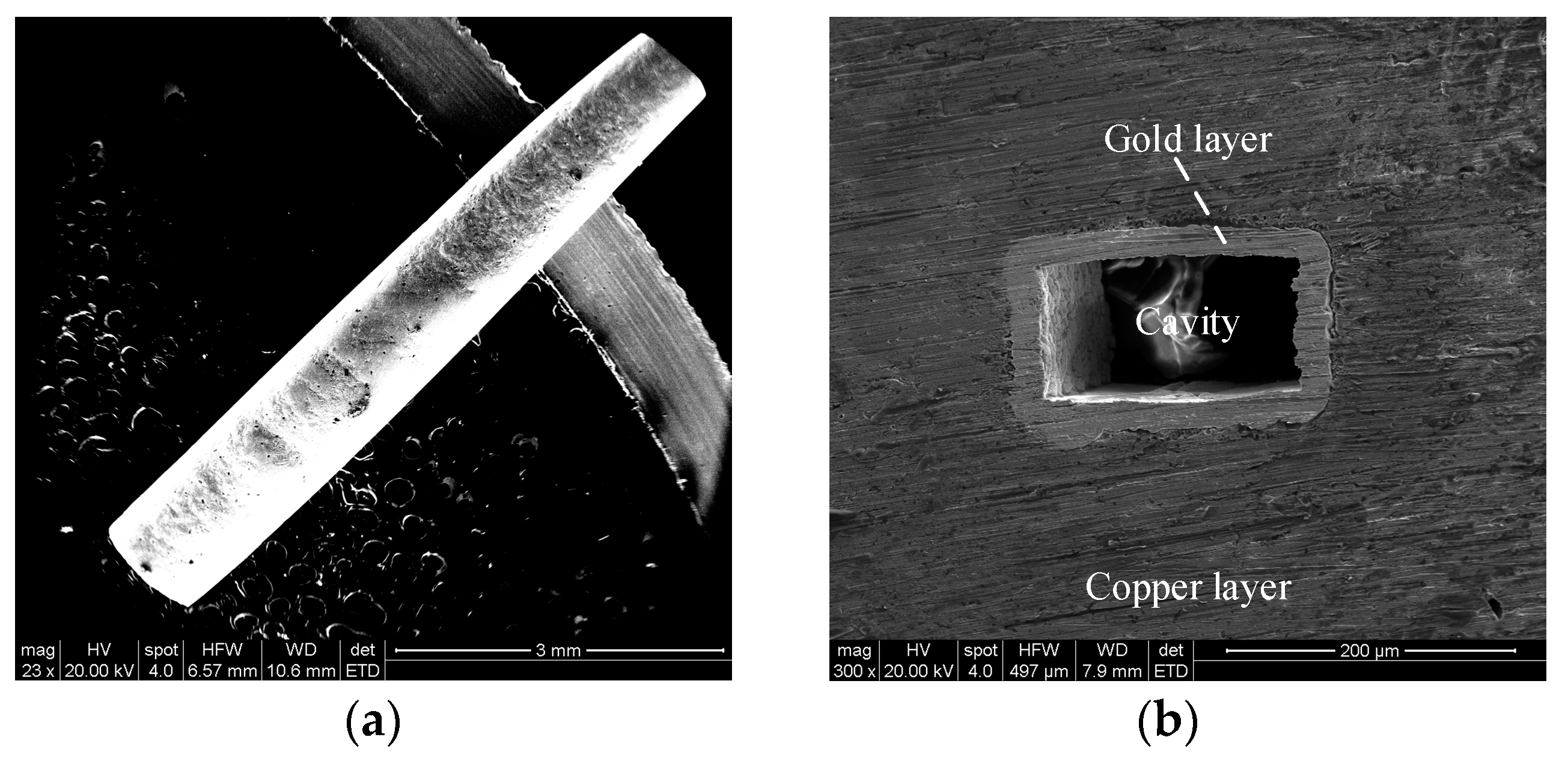
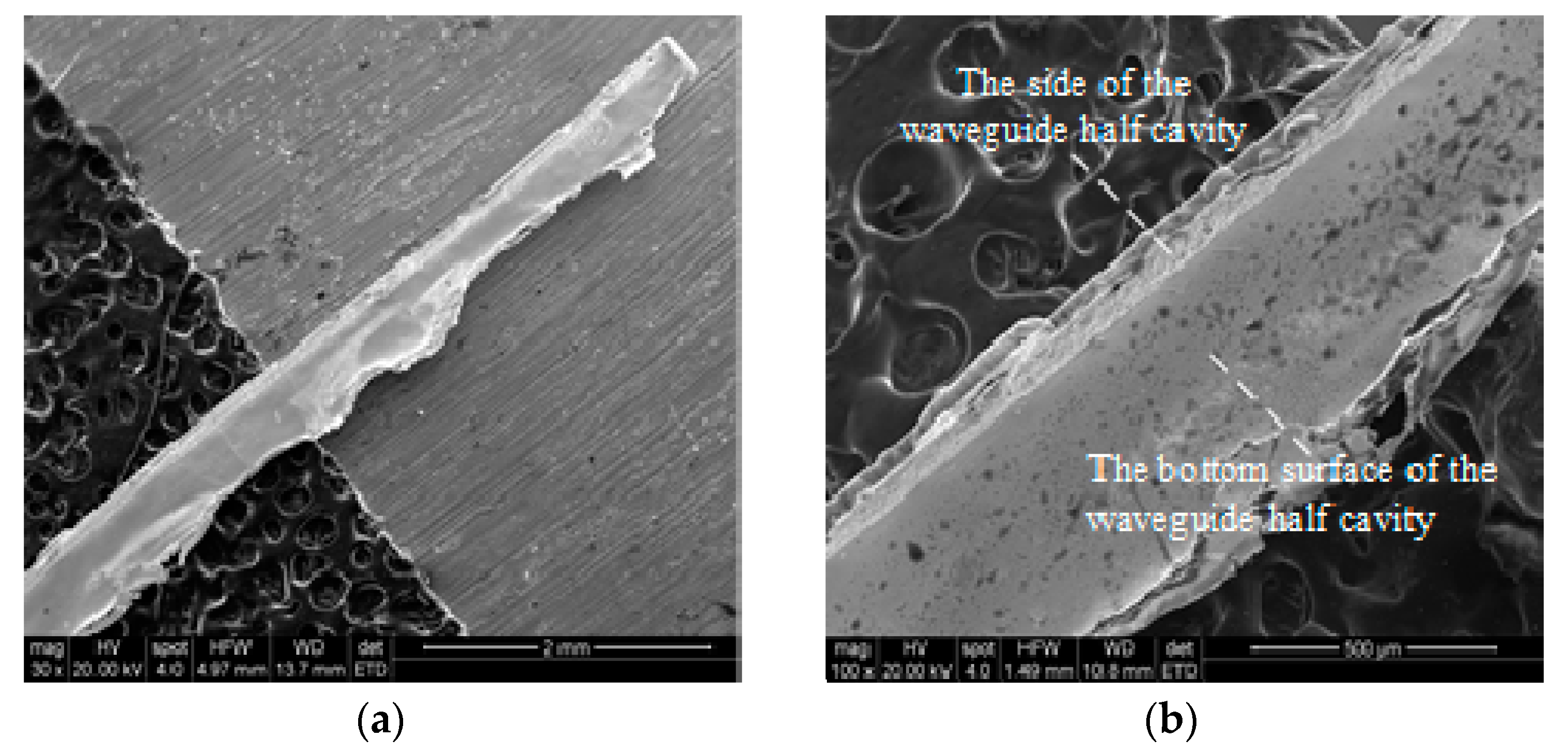
An integral 1.7 THz hollow-core metal rectangular waveguide cavity with an end-face size of 165.9 μm × 88.3 μm, an edge radius of less than 10 μm, an internal bottom surface roughness of less than 0.10 μm, and an internal side surface roughness of less than 0.40 μm was obtained. These experimental results show that this proposed manufacturing process makes it possible for the integral fabrication of terahertz rectangular cavity device structures with a high operating-frequency band.
Comparing the morphology observation results and machining measurement results of the rectangular mandrel and the waveguide cavity, the external surface morphology of the former was replicated precisely by the internal surface morphology of the latter, which indicated that the gold layer transfer technology realized the transfer of the gold layer of electrochemical deposition from the growth surface to the non-growth surface.


