
Multi-Input Logic-in-Memory for Ultra-Low Power Non-Von Neumann Computing


Department of Engineering “Enzo Ferrari”, University of Modena and Reggio Emilia, Via P. Vivarelli 10/1, 41125 Modena, Italy
*
Author to whom correspondence should be addressed.
Micromachines 2021, 12(10), 1243; https://doi.org/10.3390/mi12101243
Submission received: 8 September 2021
/
Revised: 4 October 2021
/
Accepted: 11 October 2021
/
Published: 14 October 2021
(This article belongs to the Special Issue Advances in Emerging Nonvolatile Memory)
Abstract
:Logic-in-memory (LIM) circuits based on the material implication logic (IMPLY) and resistive random access memory (RRAM) technologies are a candidate solution for the development of ultra-low power non-von Neumann computing architectures. Such architectures could enable the energy-efficient implementation of hardware accelerators for novel edge computing paradigms such as binarized neural networks (BNNs) which rely on the execution of logic operations. In this work, we present the multi-input IMPLY operation implemented on a recently developed smart IMPLY architecture, SIMPLY, which improves the circuit reliability, reduces energy consumption, and breaks the strict design trade-offs of conventional architectures. We show that the generalization of the typical logic schemes used in LIM circuits to multi-input operations strongly reduces the execution time of complex functions needed for BNNs inference tasks (e.g., the 1-bit Full Addition, XNOR, Popcount). The performance of four different RRAM technologies is compared using circuit simulations leveraging a physics-based RRAM compact model. The proposed solution approaches the performance of its CMOS equivalent while bypassing the von Neumann bottleneck, which gives a huge improvement in bit error rate (by a factor of at least 108) and energy-delay product (projected up to a factor of 1010).
1. Introduction
With the number of connected devices in use exceeding 17 billion, the volume of exchanged data rapidly rises. From this standpoint, edge computing ensures a decrease in the amount of data to be exchanged, relaxing data transfer and power constraints with obvious benefits for consumer and industrial Internet of Things (IoT), smart cities, artificial intelligence (AI), machine learning, and 5G industry. Still, its implementation requires ultra-low power hardware solutions, mainly hindered by the von Neumann bottleneck (VNB) [1,2,3], i.e., the slow and energy-hungry data transfer between CPUs and off-chip non-volatile memories. As suggested in the latest IRDS report [4], logic-in-memory (LIM) architectures that allow executing Boolean operations directly inside the memory could circumvent the VNB. Developing LIM hardware accelerators would enable the deployment at the edge of powerful and data-intensive computing paradigms such as binarized neural networks (BNNs) [5,6,7] and hyperdimensional computing [8,9,10], which strongly rely on the energy-efficient execution of logic operations. Among LIM solutions [11,12,13,14,15,16,17], circuits based on resistive memory (RRAM) technology and the implication logic (IMPLY) offer ultra-dense back end of line (BEOL) integration. Currently, the main showstoppers [12,18] hindering the introduction of RRAM-based LIM circuits are the high energy per operation (as compared to CMOS gates), the degradation of the logic values of RRAMs during circuit operation, and the need to apply very precise voltage pulses (mV accuracy may be required [12,18,19]). Moreover, while in CMOS logic multiple operations can be computed in parallel on the same inputs, in IMPLY-based LIM circuits operations are carried out sequentially. Thus, reducing the execution time is critical. Recently a novel low-power non-von Neumann LIM solution, called smart-IMPLY (SIMPLY) [20], was introduced and shown to reduce the energy per operation, to solve the problem of logic state degradation of RRAM cells, and to eliminate the need for very precise voltage pulses. Moreover, active research interest has been directed towards the study of circuit implementations of the multi-input IMPLY operation, as Siemon et al. [21] proposed the three-input IMPLY operation (named ORNOR by the authors). However, studies on circuit implementations considering the IMPLY operation generalized to more than three inputs have never been presented.
In this paper, we demonstrate the multi-input IMPLY logic scheme in the framework of SIMPLY architecture by exploiting multi-input (>2) operations, strongly reducing the execution time of complex logic functions (e.g., the set of logic operations to implement BNN inference tasks). We experimentally verify the correct circuit functionality of the core operation used in SIMPLY on TiN/Ti/HfOx/TiN devices from SEMATECH [22] (technology 4 in this work, electrical characteristics shown in Figure 1d,h). Then, for accurate and trustable results circuit simulations are performed using a fully physics-based RRAM compact model from [23,24] that includes thermal effects (also self-heating), variability, and multilevel random telegraph noise (RTN). We demonstrate the feasibility of the proposed architecture by comparing the performance obtained with three RRAM technologies from the literature (a multi-layer Pt/TiOx/HfOx/TiOx/HfOx/TiN RRAM referred to in this work as technology 1 [25,26], a TiN/HfO2/Ti/TiN RRAM technology 2 [27,28], and a TiN/HfOx/AlOx/Pt RRAM technology 3 [29]). The results obtained with all the technologies show how combining the proposed innovations allows realizing LIM circuits that outperform both existing LIM solutions and CMOS gates performance when the VNB time and energy overhead is considered, coming close to CMOS gates performance alone (excluding the VNB). Finally, we benchmark the performance improvement brought by the introduction of the multi-input IMPLY operation when executing a BNN inference task with respect to the previous IMPLY-based implementation from [30].
2. Materials and Methods
2.1. RRAM Physics-Based Compact Model for Circuit Simulations
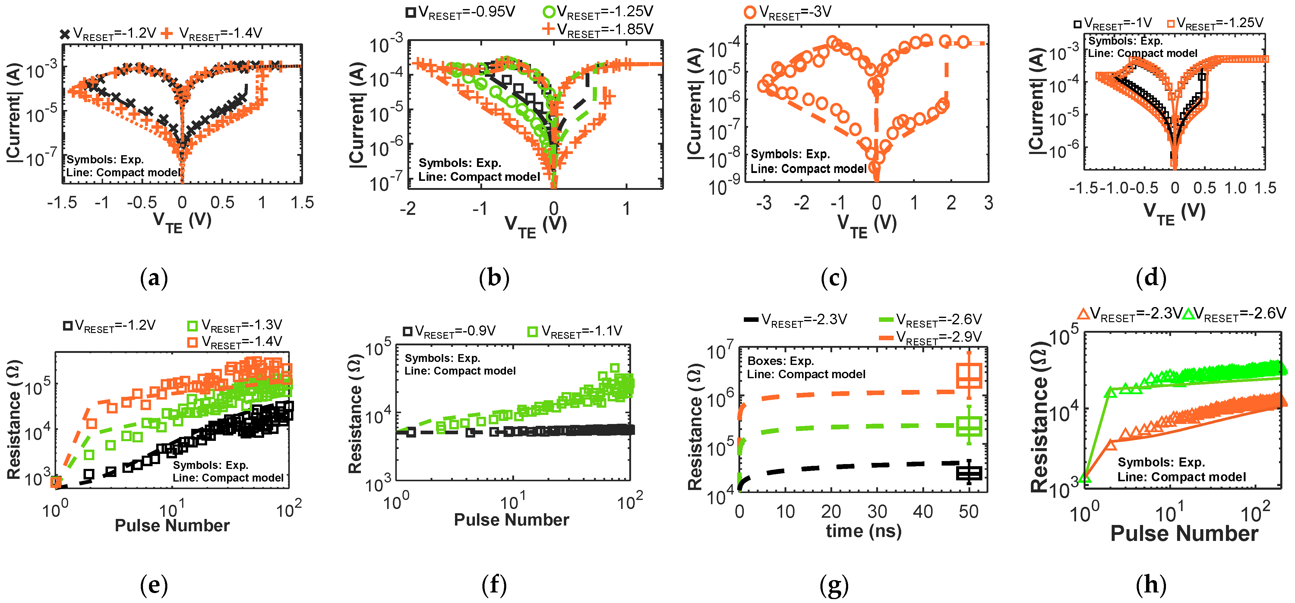
To study LIM circuits, physics-based compact models that include device non-idealities, such as device-to-device and cycle-to-cycle variability, RTN, self-heating, and thermal effects, represent a very important tool that enables achieving accurate results [18] through circuit simulations. Neglecting RRAMs nonidealities can easily result in poor circuit designs [12,18,31] with low reliability or circuits that do not work at all. In this work, we use the Verilog-A RRAM compact model from [23], which is fully physics-based and supported by the results of advanced physical multi-scale simulations. The total device resistance is modeled as the sum of a conductive filament (CF) and a dielectric barrier contribution. The barrier thickness is modeled dynamically with differential equations that reproduce the device behavior during the reset operation by considering the field-driven oxygen ions drift and recombination, and during the set operation by considering the field-accelerated bond breaking and related defect generation [23,24]. Moreover, thermal effects are modeled dynamically, considering both the thermal conductance and thermal capacitance of the CF and the barrier, thus enabling accurate predictions also when using very short pulses [18]. The model includes the intrinsic variability of both resistive states and the effects of multilevel RTN and its statistical variations [24]. In particular, to introduce cycle-to-cycle variability we add appropriate zero-mean normally distributed random noise sources on the dielectric barrier thickness during reset, and on the CF cross-section while performing a set transition [23,24]. The model, for all the four different RRAM technologies [22,25,27,29] (see Figure 1a–h) explored in this work, correctly reproduces the quasi-static IV, the response to fast reset pulses, and the experimental cycle-to-cycle variability using a single set of parameters per technology (see Figure 1 and Figure 2), thus highlighting the quality of the modeling approach and avoiding the need to design multiple parameter calibrations to reproduce the device behavior under different operating conditions. Technology 4 was experimentally characterized using the Keithley 4200-SCS parameter analyzer.
The calibrated compact model was used to perform circuit simulations with the Cadence Virtuoso® software, to determine the performance and reliability of different LIM solutions.
2.2. Logic-in-Memory with RRAM Devices and the Material Implication Logic
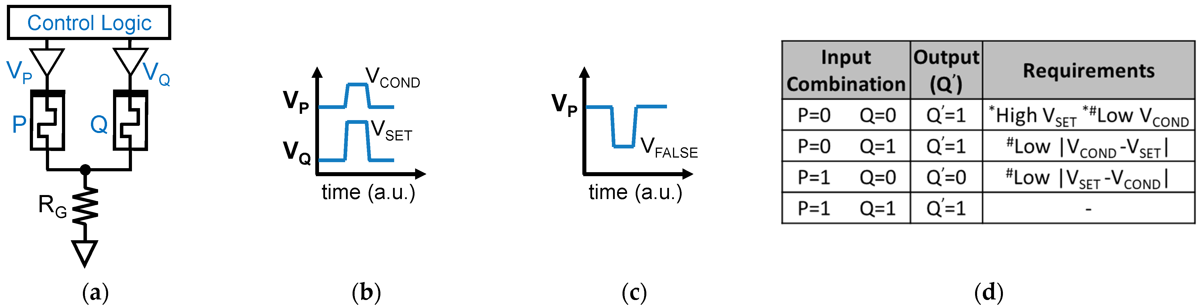
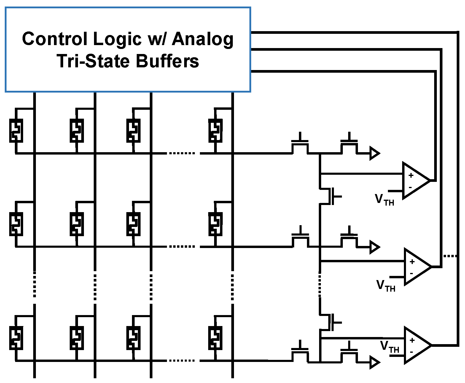
The material implication logic is a functionally complete logic that can be effectively implemented with RRAM devices [11]. In fact, RRAMs enable its efficient implementation using a circuit architecture like the one in Figure 3a. A control logic equipped with analog tri-state buffers is needed to deliver appropriate voltages at the top electrode (TE) of each RRAM device of the array, with the devices in the array having their bottom electrodes (BE) connected to the same resistor RG. Differently from traditional logic gates, in RRAM-based LIM schemes, the logic values are not encoded as voltages at circuit nodes, but as nonvolatile resistive states of RRAMs (HRS for logic 0, LRS for logic 1). All possible logic gates can be defined with two fundamental operations [32,33], namely the IMPLY (2-input 1-output operation, truth table in Figure 3d) and the FALSE (1-input 1-output operation always yielding logic 0). The COPY function (realized with IMPLY and FALSE) allows cascaded operations [12]. FALSE is executed by applying a negative voltage pulse to the RRAM (i.e., the “classical” reset operation), see Figure 3c. IMPLY between two logic values (stored in RRAMs P and Q) is executed by simultaneously applying two different positive voltage pulses at P (VCOND) and Q (VSET), see Figure 3b. The result is stored in Q, while P must preserve its state. These requirements introduce several constraints that make the design space for the definition of VSET and VCOND values very narrow [12,18], requiring a fine control down to the tens of mV, which is hard to achieve without huge overheads [12,18]. Further, the choice of RG suffers from trade-offs [12]. Moreover, the repeated execution of IMPLY causes state drifts in P and Q, eventually causing bit corruption, as reported in [12,18]. Upon this, a refresh is needed that requires moving all data back and forth to a new memory location, wasting energy and time [12,18].
2.3. The “SIMPLY” Architecture
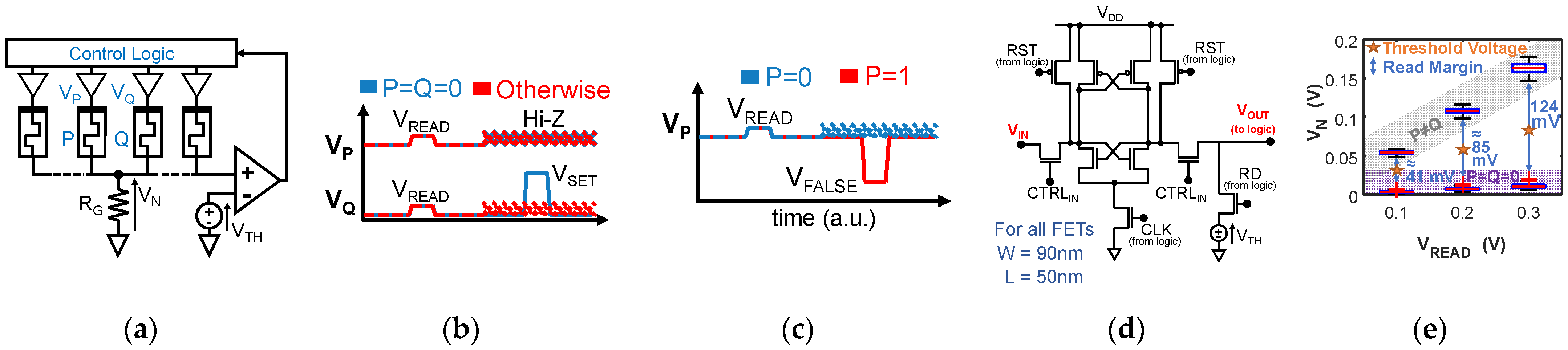
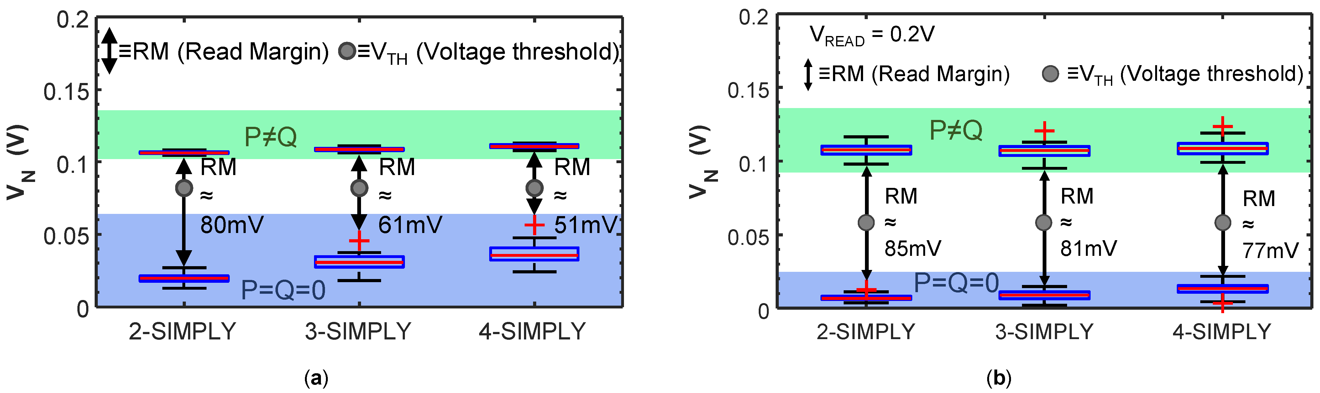
To overcome the issues of the traditional IMPLY architecture, SIMPLY was introduced in [20]. SIMPLY is based on the implication logic and originates from the observation that Q must change its state only when P = Q = 0 (case 1 of the truth table in Figure 3d). SIMPLY detects this condition by applying a small VREAD voltage pulse (200 mV in this work) to both P and Q, Figure 4b. The voltage at node N (VN, Figure 4a) is compared against a threshold (VTH) to determine if P = Q = 0. If so, the control logic which is equipped with tri-state buffers, as in the IMPLY architecture, pulses VSET on Q, keeping the driver of P at high impedance; Figure 4b, blue lines. Otherwise, both P and Q are kept at high impedance; Figure 4b, dashed red lines. The condition P = Q = 0 is easily detectable since VN is lower in this case than in all other cases, ensuring a sufficient margin (i.e., read margin—RM) also when considering RTN and variability, as shown in Figure 4e. Moreover, the RM increases with VREAD, Figure 4e, which allows trading a higher RM (i.e., lower Bit Error Rate—BER) for power, thus setting precise parameter tradeoffs. SIMPLY requires no VCOND and no fine control of the voltage pulses, overcoming the tradeoff between VSET and VCOND and the need for very precise voltage control. The problem of logic state degradation is virtually resolved, as only VREAD is applied to the devices that must retain their logic state. In fact, no degradation is observed up to (at least) 108 cycles, reducing BER by at least 108 compared to IMPLY, with no energy penalty (see Figure 5). Besides, SIMPLY needs significantly less energy as, for 3 out of 4 input combinations, only the two VREAD pulses are delivered instead of the much larger VSET and VCOND pulses, Figure 4b. To ensure high energy efficiency, we use the low-power and compact comparator design from [30], implemented in a 45-nm technology [34] (Figure 4d), which consumes 8fJ per comparison when T is in the range 0 to 85 °C and VDD is 2 V. The energy breakdown, including the comparator contribution, for all input combinations for IMPLY and SIMPLY, stresses the remarkable performance improvement, as SIMPLY reduces the energy per operation by 4× on average and up to 57× for the P = 0 Q = 1 input configuration, when considering technology 3 as an example (see Table 1). Depending on the RRAM technology, the energy consumption of the FALSE operation may be higher or lower than that of the IMPLYoperation (see Table 1 and Table 2). So, it is important to also reduce the energy of the FALSE. This can be easily done in the SIMPLY architecture, by preventing the use of the high |VFALSE| when a device is already in HRS. The state of the device is read using the same VREAD and comparator threshold used for the IMPLY operation, and the analog buffers are enabled by considering the inverted output of the comparator, see Figure 4c. This smart FALSE (sFALSE [30]) operation results in relevant energy savings (see Table 2).
In addition, both the traditional IMPLY and the SIMPLY architectures can be implemented in a crossbar array [12,30]. An example of the SIMPLY crossbar implementation is shown in Figure 6. FET devices in the array periphery are used to implement RG, to connect adjacent columns on-demand to realize COPY between any two devices, and to enable specific columns of the array. The parallel computation of SIMPLY or sFALSE operations can be implemented by increasing the number of comparators in the architecture as discussed in [30] and shown in Figure 6.
3. Results and Discussion
3.1. Multi-Input Operations: “n-SIMPLY”
In traditional static complementary CMOS logic gates, the computation of more complex operations (e.g., large fan-in operations), involves the use of additional transistors, therefore an increase in the required circuit area and complexity. In IMPLY-based architectures, the computation of complex operations instead translates to an increased number of steps of IMPLY and FALSE operations. Therefore, in these architectures, minimizing the number of steps is critical to improve the circuit performance. As suggested by theoretical works, the IMPLY logic can be extended to multi-input (>2) operations [32,35] by simultaneously applying VSET to one device (Q) and VCOND to many devices (P, S, T, …). It is only recently that the three input IMPLY operation (i.e., equivalent to the has been demonstrated by performing circuit simulations of a conventional IMPLY architecture using a physics-based compact model calibrated on a Pt/TaOx/Ta RRAM technology [21] and was shown to reduce the number of steps required for implementing a full adder. However, the reliability of the traditional IMPLY architecture worsens when the number of inputs of the IMPLY operation is increased [21]. Nevertheless, generalizing the IMPLY operation to more than three inputs allows further reducing the number of computing steps, by executing in a single step the more complex function , hereafter called n-IMPLY (n being the number of inputs) generalizing the IMPLY with 2 inputs (henceforth 2-IMPLY). Just like in 2-IMPLY, also in n-IMPLY Q must change its state to logic 1 only if all inputs are concurrently 0, that is exactly the condition detected by SIMPLY. So, n-IMPLY can be implemented in SIMPLY (henceforth n-SIMPLY) by applying VREAD to all n devices simultaneously with no architectural changes. We simulated the n-SIMPLY (with n = 2, 3, 4) for the 4 RRAM technologies explored in this work using the Cadence® Virtuoso software and verified its correct functionality by comparing the circuit parameters and energy per operation (see Table 3), including variability and RTN. While the minimum and maximum energy per n-SIMPLY operation do not change considerably for increasing values of n, the RM decreases when the number of RRAMs read in parallel increases. Nevertheless, the RM with n = 2, 3, 4 was verified to be always large enough, experimentally on technology 4 (see Figure 7a), and by using simulations on the other three technologies, as shown in Figure 7b. Moreover, in all cases, no logic state degradation is observed (see red curves in Figure 5).
3.2. Full Adder Implementation with n-SIMPLY
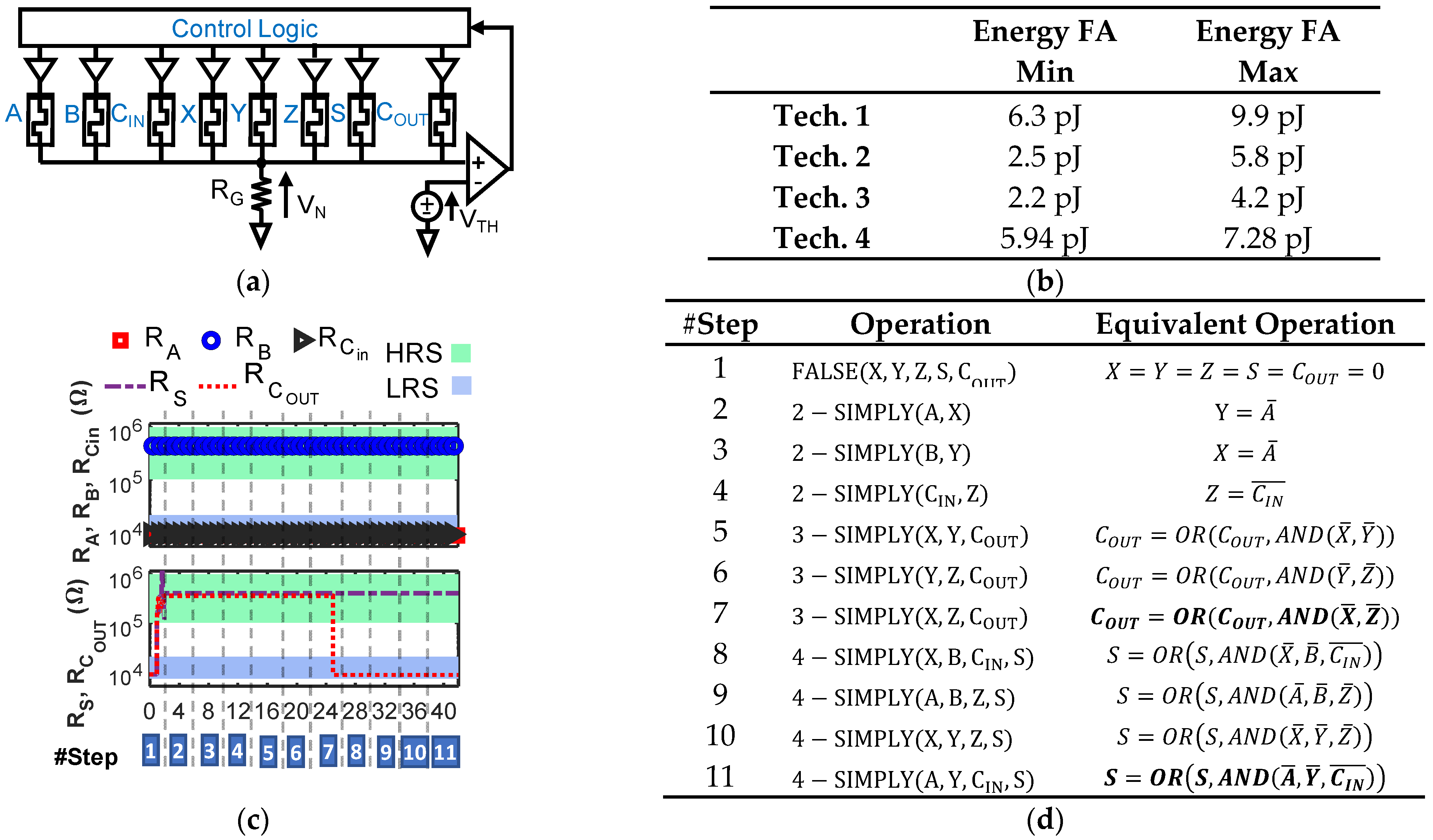
Exploiting n-SIMPLY, we propose a novel implementation of a LIM 1-bit full adder (FA). The schematic of the array and the sequence of operations are shown in Figure 8a,d. We simulated the FA at 0.5 GHz (see the example in Figure 8c) using the 4 RRAM technologies and compared the total energy consumption (including the comparator and the effects of variability and RTN) in Figure 8b. Not surprisingly, technology 3 [29], which is the technology with the lowest current compliance (IC = 100 µA, see Figure 1c), results in the lowest energy consumption. We considered the worst-case result (i.e., Energy FA max column in Figure 8b) obtained with technology 3 and benchmarked it in detail against existing LIM solutions in the literature and its CMOS counterpart in Table 4 and Table 5, respectively. Considering the worst-case energy contribution for each 1-bit FA operation results in an energy consumption overestimation, that, as a first-order approximation, provides enough room to account for additional energy dissipated by components in the peripheral circuitry that were not included in the circuit simulations (i.e., the analog tri-state buffers). The proposed FA outperforms all existing IMPLY-based LIM solutions (both simulation and experimental works [12,20,36,37,38]), in terms of the number of steps (delay) and energy consumption, using few devices and lowering the energy-delay product (EDP) by a factor >103, bringing it much closer to the CMOS one. We compare the performance of the proposed solution vs. CMOS (with and without considering the VNB energy and time overhead) in Table 5 considering the parallel execution of 512 32-bit FA operations (simple ripple carry architecture), which entails 4kB data, which is the common memory page size [39].
The proposed solution strongly outperforms different CMOS FA solutions [40,41,42] (>106 improvement in EDP) when VNB data exchange overhead [39] is included. Projections show that substantial improvements are obtained by using devices formed at lower IC [43] and shorter pulses [44], as in Table 5, achieving the performance of CMOS gates without the huge VNB penalty (up to a ≈2.4 × 10¹⁰ improvement in EDP as compared to a CMOS FA that suffers from VNB).
3.3. Binarized Neural Networks Applications
As the adoption of deep learning and neural networks is becoming more and more pervasive, the demand for energy efficient hardware accelerators is rapidly growing. When considering neural networks, the most effective way to improve energy efficiency is to avoid the VNB by performing computations in-memory [45,46,47,48]. A common approach exploits resistive memory crossbar arrays to implement in analog the vector matrix multiplication in a single step [45]. However, reliability issues affecting RRAM devices, such as the large cycle-to-cycle variability, limit the number of bits that can be reliably stored in a single device [49] thus suggesting that low-bit precision neural networks are a more suitable solution for the current state of the art RRAM devices. The extreme case of low-bit precision neural networks are BNNs, which have been shown to retain high classification accuracy despite the use of single-bit neuron weights and activations [5,50,51]. While the in-memory computation of the analog vector matrix multiplication is extremely attractive [6,7,50,52], it has some limitations and tradeoffs. In fact, this approach lacks the possibility to reconfigure the type of operation to be computed in-memory.
Since neurons in BNNs perform logic operations, the BNNs inference can be implemented in the SIMPLY architecture, as shown in [30] where a BNN was implemented using the 2-SIMPLY. Compared to an analog implementation, the SIMPLY architecture trades reconfigurability for larger computation latency. To address the higher latency issue, the multi-input IMPLY operation can be used as discussed below.
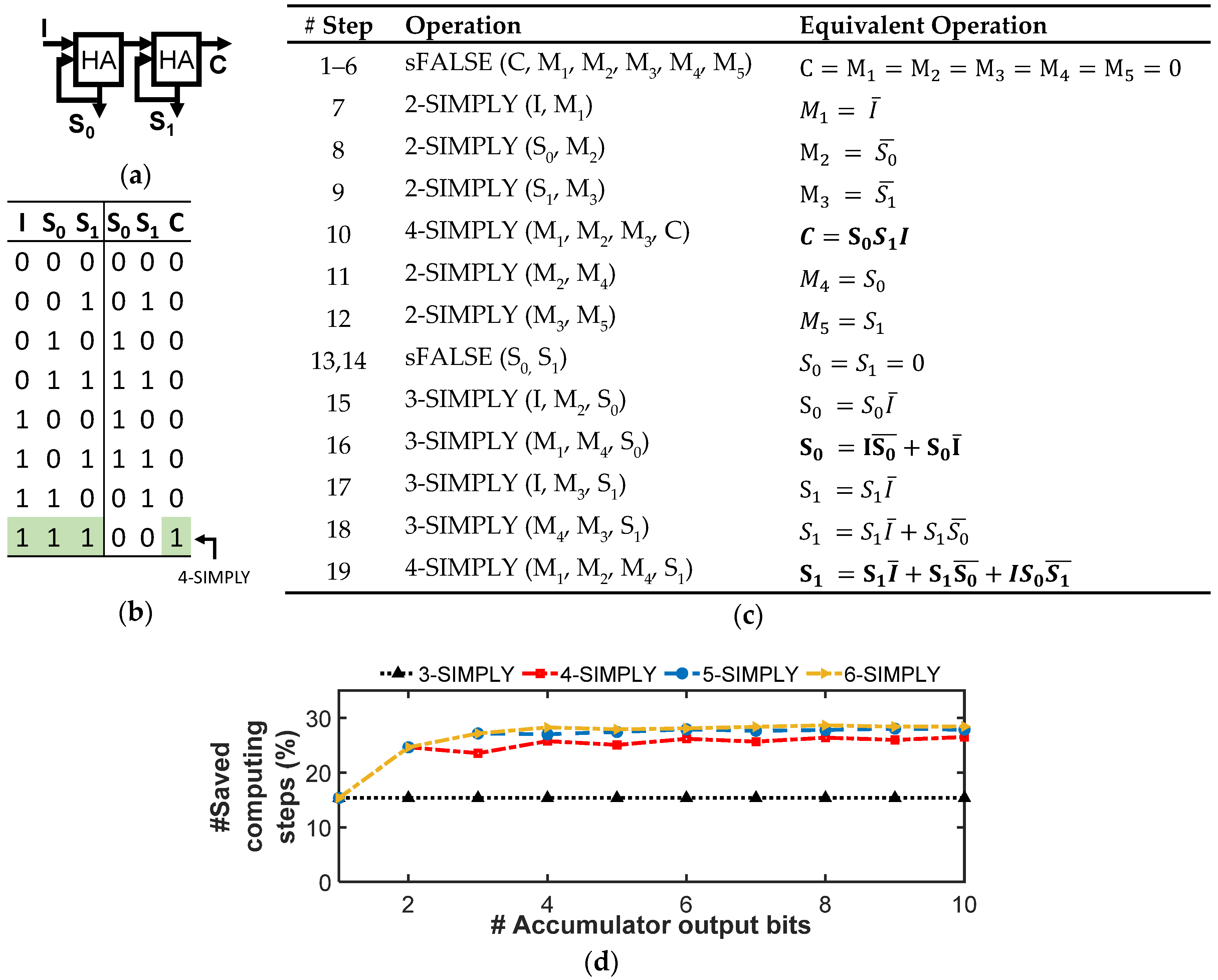
As shown in [30], in BNNs, multiplications between the inputs and each neuron’s weights are implemented with bitwise XNOR operations, the accumulation as the popcount operation, and the activation as a comparison with a trained threshold. In addition, batch normalization layers can be implemented with full adders for which we have already discussed the optimized n-SIMPLY implementation. The effectiveness of the multi-input IMPLY operation in reducing the number of computing steps is analyzed for each logic function since it is strongly dependent on the associated specific sequence of operations. As shown in Figure 9, by using the 3-SIMPLY the XNOR operation is computed in 5 steps while using a single additional device, instead of requiring 9 steps and 2 additional support devices when using only the 2-SIMPLY. For the popcount and activation function operations, different optimization strategies that minimize the number of computing steps for different fan-in (i.e., n) of the n-SIMPLY operation can be employed. As shown in [30], the accumulator can be implemented as a chain of log2(#input bits) 1-bit half adders (HAs) where the first HA receives in input the bit that needs to be accumulated and its current output (i.e., S0 in Figure 10a), while the following HAs receive at their inputs the carry-out from the previous HA and their current output (i.e., as in in Figure 10a but also for more than two HAs). When accumulating a sequence of bits, all the bits are input sequentially to the HA representing the LSB. The operations of the subsequent HAs are performed only after a number of input bits equal to their relative bit position have been summed (e.g., HA with bit position 3 is activated only after 23 input bits have been summed). Thus, the length of the HA chain grows as more input bits have been summed. By using the 3-SIMPLY operation, the number of steps for each HA operation is reduced from 13 to 11, see Supplementary Figure S1. An effective strategy that can further reduce the total number of computing steps involves the use of the n-SIMPLY operation to compute the equivalent logic function resulting from a sequence of more than one 1-bit HAs. Thereby, the equivalent carry-out of a sequence of more than 1 HA (output C in Figure 10a), can be computed in a single step by exploiting the n-SIMPLY operation (with n = #HAs + 2). For instance, the carry-out can be computed with a 4-SIMPLY or a 5-SIMPLY when a sequence of 2 or 3 HAs is considered, respectively. Moreover, the number of intermediate computing steps required to calculate the output bits Si (see Figure 10a) is reduced using the n-SIMPLY, as shown in Figure 10b and Supplementary Figure S2–S4, where the sequence of operations computing the result of a sequence of 2, 3, and 4 HAs are reported. Specifically, 19 (see Figure 10c), 28 (see Supplementary Figure S3), and 37 computing steps (see Supplementary Figure S4), for a sequence of 2, 3, and 4 HAs, respectively, are required instead of 26, 39, and 52 steps when using only the 2-SIMPLY. The overall number of computing steps scales rapidly with the number of output bits, but the use of n-SIMPLY with n up to 3 (i.e., only the chain of 2 HAs is optimized) provides a saving of around 15% of steps while for n > 3 leads to a step saving above 25%. However, most of the reduction in the number of computing steps is achieved when using n-SIMPLY with n up to 4 while the use of n > 4 provides only a limited improvement, as shown in Figure 10d, that does not justify the risk of reducing the reliability of the circuit due to the smaller available RMs.
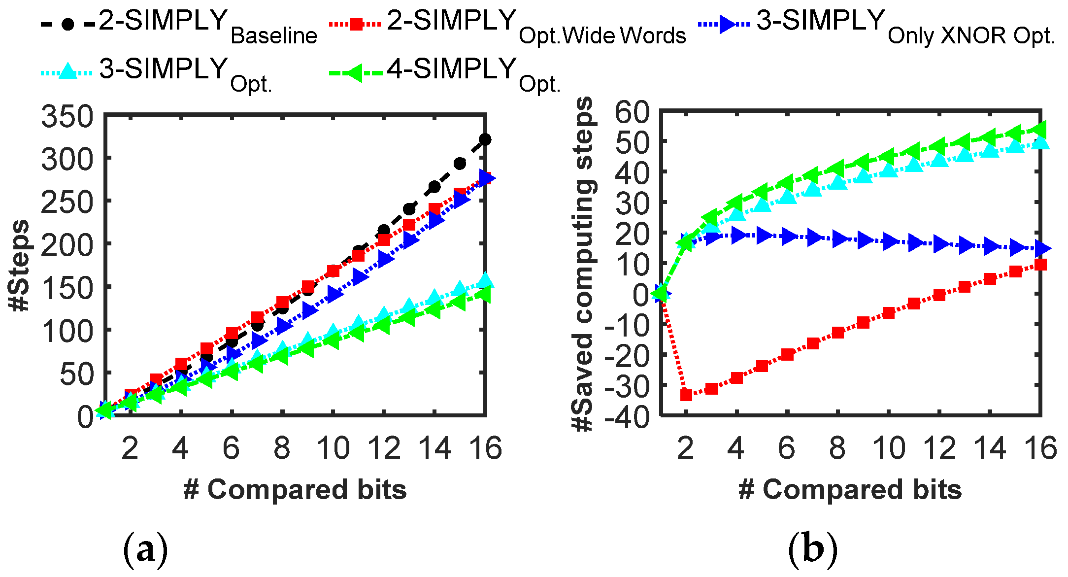
For the activation (i.e., comparison with a trained threshold), we improved the 2-SIMPLY implementation from [30], by removing unnecessary computing steps. The resulting sequence of computing steps can be built using the flowchart reported in Supplementary Figure S5, which consists in the computation of a bitwise XNOR between the input and the trained threshold, and additional AND/OR operations. By following this method, the number of computing steps scales exponentially with the number of compared input bits (i.e., 2-SIMPLYbaseline in Figure 11). Thus, we also consider an alternative approach in which the number of computing steps scales linearly with the number of input bits, reducing the number of computing steps when more than 9 bits are compared (see 2-SIMPLYOpt.WideWords in Figure 11 and Supplementary Figure S6). The same two approaches can be optimized with the 3-SIMPLY operation (see 3-SIMPLYOnlyXNOROpt. and 3-SIMPLYOpt.) providing a considerable reduction in the number of computing steps (see Supplementary Figures S7 and S8). While the use of the 4-SIMPLY operation enables additional step savings (see 4-SIMPLYOpt. in Figure 11 and Supplementary Figure S9), n-SIMPLY with larger n values would not provide any additional step reduction.
Thus, some applications, such as the BNN inference, can largely benefit from a limited increase in n-SIMPLY operation parallelism. In fact, most of the step reduction for a 1-bit FA, the bitwise XNOR operation, the popcounting operation, and the activation function are achieved by using only up to the 4-SIMPLY operation. Further increasing the parallelism of the n-SIMPLY operation would not provide relevant additional energy savings while causing a reduction in the available RM, thus potentially reducing the circuit reliability, and increasing the instruction set complexity.
To benchmark the latency improvement brought by the n-SIMPLY operation when performing an inference task, we consider the results of the 2-SIMPLY implementation of a BNN reported in [30], which consists of a single fully connected hidden layer with 1000 neurons performing a handwritten digit recognition task, achieving an accuracy of 91.4%. The use of n-SIMPLY reduces the number of computing steps from 190,657 to 135,539, therefore resulting in a remarkable 29% latency reduction leading to a 542 µs inference time at 0.5 GHz, which further highlights the advantages of the SIMPLY architecture as a solution for ultra-low power devices for edge computing applications.
Additionally, unlike conventional IMPLY architectures, SIMPLY is not constrained to employ bipolar RRAM devices [18] and can use unipolar RRAM devices as well as other memory technologies such as phase change memories (PCM) [53], ferroelectric FETs (FeFETs) [54], ferroelectric tunnel junctions (FTJs) [54], and virtually any 2- or 3-terminal non-volatile memory. Therefore, device/circuit co-design strategies can be implemented easily to further improve performance. For instance, memory technologies with ultra-low power consumption like FeFETs and FTJs [54] may be targeted to improve power consumption. Further, devices with higher endurance than most RRAM technologies, such as PCM [54] and STT-MRAM [53], could be evaluated on the SIMPLY architecture.
4. Conclusions
In this work, we presented the advantages of the multi-input IMPLY operation performed on SIMPLY (n-SIMPLY), a new LIM edge computing architecture that overcomes all the relevant issues of traditional IMPLY solutions. The advantages of multi-input SIMPLY operations were analyzed in detail using a comprehensive physics-based RRAM compact model calibrated on three different RRAM technologies in the literature and validated by the experimental analysis carried out on fabricated devices. The performance comparison of a 1-bit full adder based on n-SIMPLY and state-of-the-art LIM alternatives present in the literature shows that n-SIMPLY allows realizing a LIM solution that approaches the performance of CMOS gates while bypassing VNB, with a huge improvement in BER (by a factor of at least 108) and EDP (up to a factor 1010). Moreover, we analyze the advantages brought by n-SIMPLY on a BNN inference task and show that it enables a latency reduction of 29% with respect to previous studies.
Supplementary Materials
The following are available online at https://www.mdpi.com/article/10.3390/mi12101243/s1, Figure S1: 1-bit HA sequence of computing steps using (a) 2-SIMPLY only and, (b) up to 3-SIMPLY. The use of 3-SIMPLY reduces the number of computing steps from 13 to 11. Figure S2. 4-SIMPLY-based implementation of two concatenated 1-bit HAs that are used to implement the popcounting operation for BNNs. (a) Sketch of the two serially connected half-adders (HAs). (b) Sequence of IMPLY and FALSE operations implementing the result of the operation. The use of 4-SIMPLY reduces the number of computing steps from 26 (when using only the 2-SIMPLY Figure S1a) to 19. Figure S3. 5-SIMPLY-based implementation of three concatenated 1-bit HAs that are used to implement the popcounting operation for BNNs. (a) Sketch of the three serially connected half-adders (HAs). (b) Sequence of IMPLY and FALSE operations implementing the result of the operation. The use of 5-SIMPLY reduces the number of computing steps from 39 (when using only the 2-SIMPLY Figure S1a) to 28. Figure S4. 6-SIMPLY-based implementation of four concatenated 1-bit HAs that are used to implement the popcounting operation for BNNs. (a) Sketch of the four serially connected half-adders (HAs). (b) Sequence of IMPLY and FALSE operations implementing the result of the operation. The use of 6-SIMPLY reduces the number of computing steps from 52 (when using only the 2-SIMPLY Figure S1a) to 37. Figure S5. Flowchart building the sequence of computing steps required for implementing the activation function of a BNN neuron, i.e., the comparison with a threshold (TH), when using the 2-SIMPLY operation (i.e., 2-SIMPLY-baseline in Figure 11). The formula for the comparison operation is reported together with the scaling of the number of computing steps (i.e., #steps) as a function of the number of compared input bits (n). Figure S6. Flowchart building the sequence of computing steps optimized for large number of input bits, that is used to implement the activation function of a BNN neuron, i.e., the comparison with a threshold (TH), when using the 2-SIMPLY operation (i.e., 2-SIMPLY Opt. Wide Words in Figure 11). The formula for the comparison operation is reported together with the scaling of the number of computing steps (i.e., #steps) as a function of the number of compared input bits (n). Figure S7. Flowchart building the sequence of computing steps that is used to implement the activation function of a BNN neuron, i.e., the comparison with a threshold (TH), when using the 3-SIMPLY operation and optimizing only the steps required for computing the intermediate XNOR operations (i.e., 3-SIMPLY Only XNOR in Figure 11). The formula for the comparison operation is reported together with the scaling of the number of computing steps (i.e., #steps) as a function of the number of compared input bits (n). Figure S8. Flowchart building the optimized sequence of computing steps that is used to implement the activation function of a BNN neuron, i.e., the comparison with a threshold (TH), when using the 3-SIMPLY operation (i.e., 3-SIMPLY Opt. in Figure 11). The formula for the comparison operation is reported together with the scaling of the number of computing steps (i.e., #steps) as a function of the number of compared input bits (n). Figure S9. Flowchart building the optimized sequence of computing steps that is used to implement the activation function of a BNN neuron, i.e., the comparison with a threshold (TH), when using the 4-SIMPLY operation (i.e., 4-SIMPLY Opt. in Figure 11). The formula for the comparison operation is reported together with the scaling of the number of computing steps (i.e., #steps) as a function of the number of compared input bits (n).
Author Contributions
Conceptualization, T.Z. and F.M.P.; methodology, T.Z.; software, T.Z., F.M.P. and P.P; validation, T.Z.; writing—original draft preparation, T.Z. and F.M.P.; writing—review and editing, T.Z., F.M.P. and P.P; supervision, F.M.P. and P.P. All authors have read and agreed to the published version of the manuscript.
Funding
This research received no external funding.
Conflicts of Interest
The authors declare no conflict of interests.
References
- Backus, J. Can programming be liberated from the von Neumann style? A functional style and its algebra of programs. Commun. ACM 1978, 21, 613–641. [Google Scholar] [CrossRef] [Green Version]
- Zidan, M.; Strachan, J.P.; Lu, W.D. The future of electronics based on memristive systems. Nat. Electron. 2018, 1, 22–29. [Google Scholar] [CrossRef]
- Kvatinsky, S. Real Processing-in-memory with memristive Memory Processing Unit (mMPU). In Proceedings of the 2019 IEEE 30th International Conference on Application-specific Systems, Architectures and Processors (ASAP), New York, NY, USA, 15–17 July 2019; Volume 2160-052X, pp. 142–148. [Google Scholar]
- International Roadmap for Devices and Systems (IRDSTM) 2020 Edition—IEEE International Roadmap for Devices and SystemsTM. Available online: https://irds.ieee.org/editions/2020 (accessed on 19 March 2020).
- Courbariaux, M.; Hubara, I.; Soudry, D.; El-Yaniv, R.; Bengio, Y. Binarized Neural Networks: Training Deep Neural Networks with Weights and Activations Constrained to +1 or −1. arXiv 2016, arXiv:1602.02830. [Google Scholar]
- Yu, S.; Li, Z.; Chen, P.; Wu, H.; Gao, B.; Wang, D.; Wu, W.; Qian, H. Binary neural network with 16 Mb RRAM macro chip for classification and online training. In Proceedings of the 2016 IEEE International Electron Devices Meeting (IEDM), San Francisco, CA, USA, 3–7 December 2016; pp. 16.2.1–16.2.4. [Google Scholar]
- Sun, X.; Peng, X.; Chen, P.; Liu, R.; Seo, J.; Yu, S. Fully parallel RRAM synaptic array for implementing binary neural network with (+1, −1) weights and (+1, 0) neurons. In Proceedings of the 2018 23rd Asia and South Pacific Design Automation Conference (ASP-DAC), Jeju, Korea, 22–25 January 2018; pp. 574–579. [Google Scholar]
- Karunaratne, G.; Le Gallo, M.; Cherubini, G.; Benini, L.; Rahimi, A.; Sebastian, A. In-memory hyperdimensional computing. Nat. Electron. 2020, 3, 327–337. [Google Scholar] [CrossRef]
- Kanerva, P. Hyperdimensional Computing: An Introduction to Computing in Distributed Representation with High-Dimensional Random Vectors. Cogn. Comput. 2009, 1, 139–159. [Google Scholar] [CrossRef]
- Burrello, A.; Schindler, K.; Benini, L.; Rahimi, A. One-shot learning for iEEG seizure detection using end-to-end binary operations: Local binary patterns with hyperdimensional computing. In Proceedings of the 2018 IEEE Biomedical Circuits and Systems Conference (BioCAS), Cleveland, OH, USA, 17–19 October 2018. [Google Scholar] [CrossRef] [Green Version]
- Borghetti, J.; Snider, G.S.; Kuekes, P.J.; Yang, J.J.; Stewart, D.R.; Williams, R.S. ‘Memristive’ Switches Enable ‘Stateful’ Logic Operations via Material Implication. Nature 2010, 464, 873. [Google Scholar] [CrossRef] [PubMed]
- Kvatinsky, S.; Satat, G.; Wald, N.; Friedman, E.G.; Kolodny, A.; Weiser, U.C. Memristor-Based Material Implication (IMPLY) Logic: Design Principles and Methodologies. IEEE Trans. Very Large Scale Integr. (VLSI) Syst. 2013, 22, 2054–2066. [Google Scholar] [CrossRef]
- Kvatinsky, S.; Belousov, D.; Liman, S.; Satat, G.; Wald, N.; Friedman, E.G.; Kolodny, A.; Weiser, U.C. MAGIC—Memristor-Aided Logic. IEEE Trans. Circuits Syst. II Express Briefs 2014, 61, 895–899. [Google Scholar] [CrossRef]
- Yu, J.; Du Nguyen, H.A.; Abu Lebdeh, M.; Taouil, M.; Hamdioui, S. Enhanced scouting logic: A robust memristive logic design scheme. In Proceedings of the 2019 IEEE/ACM International Symposium on Nanoscale Architectures (NANOARCH), Qingdao, China, 17–19 July 2019; pp. 1–6. [Google Scholar]
- Reuben, J. Rediscovering Majority Logic in the Post-CMOS Era: A Perspective from In-Memory Computing. J. Low Power Electron. Appl. 2020, 10, 28. [Google Scholar] [CrossRef]
- Moreau, M.; Muhr, E.; Bocquet, M.; Aziza, H.; Portal, J.; Giraud, B.; Noël, J. Reliable ReRAM-based logic operations for computing in memory. In Proceedings of the 2018 IFIP/IEEE International Conference on Very Large Scale Integration (VLSI-SoC), Verona, Italy, 8–10 October 2018; pp. 192–195. [Google Scholar]
- Xie, L.; Du Nguyen, H.A.; Yu, J.; Kaichouhi, A.; Taouil, M.; AlFailakawi, M.; Hamdioui, S. Scouting logic: A novel memristor-based logic design for resistive computing. In Proceedings of the 2017 IEEE Computer Society Annual Symposium on VLSI (ISVLSI), Bochum, Germany, 3–5 July 2017; pp. 176–181. [Google Scholar]
- Zanotti, T.; Puglisi, F.M.; Pavan, P. Reliability-Aware Design Strategies for Stateful Logic-in-Memory Architectures. IEEE Trans. Device Mater. Reliab. 2020, 20, 278–285. [Google Scholar] [CrossRef]
- Hoffer, B.; Rana, V.; Menzel, S.; Waser, R.; Kvatinsky, S. Experimental Demonstration of Memristor-Aided Logic (MAGIC) Using Valence Change Memory (VCM). IEEE Trans. Electron. Devices 2020, 67, 3115–3122. [Google Scholar] [CrossRef]
- Zanotti, T.; Puglisi, F.M.; Pavan, P. Smart Logic-in-Memory Architecture for Low-Power Non-Von Neumann Computing. IEEE J. Electron. Devices Soc. 2020, 8, 757–764. [Google Scholar] [CrossRef]
- Siemon, A.; Drabinski, R.; Schultis, M.J.; Hu, X.; Linn, E.; Heittmann, A.; Waser, R.; Querlioz, D.; Menzel, S.; Friedman, J.S. Stateful Three-Input Logic with Memristive Switches. Sci. Rep. 2019, 9, 14618. [Google Scholar] [CrossRef] [Green Version]
- Larcher, L.; Puglisi, F.M.; Pavan, P.; Padovani, A.; Vandelli, L.; Bersuker, G. A Compact Model of Program Window in HfOx RRAM Devices for Conductive Filament Characteristics Analysis. IEEE Trans. Electron. Devices 2014, 61, 2668–2673. [Google Scholar] [CrossRef]
- Puglisi, F.M.; Zanotti, T.; Pavan, P. Unimore Resistive Random Access Memory (RRAM) Verilog-A Model. nanoHUB 2019. [Google Scholar] [CrossRef]
- Zanotti, T.; Puglisi, F.M.; Pavan, P. Low-Bit precision neural network architecture with high immunity to variability and random telegraph noise based on resistive memories. In Proceedings of the 2021 IEEE International Reliability Physics Symposium (IRPS), Monterey, CA, USA, 21–25 March 2021; pp. 1–6. [Google Scholar] [CrossRef]
- Yu, S.; Gao, B.; Fang, Z.; Yu, H.; Kang, J.; Wong, H.-P. A neuromorphic visual system using RRAM synaptic devices with Sub-PJ energy and tolerance to variability: Experimental characterization and large-scale modeling. In Proceedings of the 2012 International Electron Devices Meeting, San Francisco, CA, USA, 10–13 December 2012; pp. 10.4.1–10.4.4. [Google Scholar]
- Fang, Z.; Yu, H.Y.; Li, X.; Singh, N.; Lo, G.Q.; Kwong, D.L. HfOx/TiOx/HfOx/TiOx Multilayer-Based Forming-Free RRAM Devices with Excellent Uniformity. IEEE Electron. Device Lett. 2011, 32, 566–568. [Google Scholar] [CrossRef]
- Woo, J.; Moon, K.; Song, J.; Lee, S.; Kwak, M.; Park, J.; Hwang, H. Improved Synaptic Behavior Under Identical Pulses Using AlOx/HfO2Bilayer RRAM Array for Neuromorphic Systems. IEEE Electron. Device Lett. 2016, 37, 994–997. [Google Scholar] [CrossRef]
- Woo, J.; Song, J.; Moon, K.; Lee, S.; Park, J.; Hwang, H. Multilevel conductance switching of a HfO2 RRAM array induced by controlled filament for neuromorphic applications. In Proceedings of the 2016 IEEE Silicon Nanoelectronics Workshop (SNW), Honolulu, HI, USA, 12–13 June 2016; pp. 40–41. [Google Scholar] [CrossRef]
- Yu, S.; Wu, Y.; Chai, Y.; Provine, J.; Wong, H.-S.P. Characterization of switching parameters and multilevel capability in HfOx/AlOx bi-layer RRAM devices. In Proceedings of the 2011 International Symposium on VLSI Technology, Systems and Applications, Hsinchu, Taiwan, 25–27 April 2011; pp. 1–2. [Google Scholar] [CrossRef]
- Zanotti, T.; Puglisi, F.M.; Pavan, P. Reliability and Performance Analysis of Logic-in-Memory Based Binarized Neural Networks. IEEE Trans. Device Mater. Reliab. 2021, 21, 183–191. [Google Scholar] [CrossRef]
- Li, H.; Jiang, Z.; Huang, P.; Wu, Y.; Chen, H.-Y.; Gao, B.; Liu, X.Y.; Kang, J.F.; Wong, H.-S.P. Variation-aware, reliability-emphasized design and optimization of RRAM using SPICE model. In Proceedings of the 2015 Design, Automation & Test in Europe Conference & Exhibition (DATE), Grenoble, France, 9–13 March 2015. [Google Scholar] [CrossRef]
- Lehtonen, E.; Poikonen, J.; Laiho, M. Two memristors suffice to compute all Boolean functions. Electron. Lett. 2010, 46, 230–231. [Google Scholar] [CrossRef]
- Poikonen, J.H.; Lehtonen, E.; Laiho, M. On Synthesis of Boolean Expressions for Memristive Devices Using Sequential Implication Logic. IEEE Trans. Comput. Des. Integr. Circuits Syst. 2012, 31, 1129–1134. [Google Scholar] [CrossRef]
- Stine, J.E.; Castellanos, I.; Wood, M.; Henson, J.; Love, F.; Davis, W.R.; Franzon, P.D.; Bucher, M.; Basavarajaiah, S.; Oh, J.; et al. FreePDK: An open-source variation-aware design kit. In Proceedings of the 2007 IEEE International Conference on Microelectronic Systems Education (MSE’07), San Diego, CA, USA, 3–4 June 2007; pp. 173–174. [Google Scholar]
- Marranghello, F.S.; Callegaro, V.; Martins, M.G.A.; Reis, A.I.; Ribas, R.P. Factored Forms for Memristive Material Implication Stateful Logic. IEEE J. Emerg. Sel. Top. Circuits Syst. 2015, 5, 267–278. [Google Scholar] [CrossRef]
- Cheng, L.; Zhang, M.-Y.; Li, Y.; Zhou, Y.-X.; Wang, Z.-R.; Hu, S.-Y.; Long, S.-B.; Liu, M.; Miao, X.-S. Reprogrammable logic in memristive crossbar for in-memory computing. J. Phys. D Appl. Phys. 2017, 50, 505102. [Google Scholar] [CrossRef]
- Junsangsri, P.; Han, J.; Lombardi, F. Logic-in-Memory with a Nonvolatile Programmable Metallization Cell. IEEE Trans. Very Large Scale Integr. (VLSI) Syst. 2015, 24, 1. [Google Scholar] [CrossRef]
- Lehtonen, E.; Poikonen, J.; Laiho, M. Implication logic synthesis methods for memristors. In Proceedings of the 2012 IEEE International Symposium on Circuits and Systems, Seoul, Korea, 20–23 May 2012; pp. 2441–2444. [Google Scholar]
- Park, S.; Jung, D.; Kang, J.; Kim, J.; Lee, J. CFLRU: A replacement algorithm for flash memory. In CASES ’06: Proceedings of the 2006 International Conference on Compilers, Architecture and Synthesis for Embedded Systems; ACM: New York, NY, USA, 2006; pp. 234–241. [Google Scholar]
- Aguirre-Hernandez, M.; Linares-Aranda, M. CMOS Full-Adders for Energy-Efficient Arithmetic Applications. IEEE Trans. Very Large Scale Integr. (VLSI) Syst. 2010, 19, 718–721. [Google Scholar] [CrossRef]
- Yadav, A.K.; Shrivatava, B.P.; Dadoriya, A.K. low power high speed 1-bit full Adder circuit design at 45 nm CMOS technology. In Proceedings of the 2017 International Conference on Recent Innovations in Signal processing and Embedded Systems (RISE), Bhopal, India, 27–29 October 2017; pp. 427–432. [Google Scholar]
- Sharma, S.; Soni, G. Comparision analysis of FinFET based 1-bit full Adder cell implemented using different logic styles at 10, 22 and 32 NM. In Proceedings of the 2016 International Conference on Energy Efficient Technologies for Sustainability (ICEETS), Nagercoil, India, 7–8 April 2016; pp. 660–667. [Google Scholar]
- Zhou, J.; Cai, F.; Wang, Q.; Chen, B.; Gaba, S.; Lu, W.D. Very Low-Programming-Current RRAM With Self-Rectifying Characteristics. IEEE Electron. Device Lett. 2016, 37, 404–407. [Google Scholar] [CrossRef]
- Wang, C.; Wu, H.; Gao, B.; Wu, W.; Dai, L.; Li, X.; Qian, H. Ultrafast RESET Analysis of HfOx -Based RRAM by Sub-Nanosecond Pulses. Adv. Electron. Mater. 2017, 3, 1700263. [Google Scholar] [CrossRef]
- Tsai, H.-Y.; Ambrogio, S.; Narayanan, P.; Shelby, R.M.; Burr, G.W. Recent progress in analog memory-based accelerators for deep learning. J. Phys. D Appl. Phys. 2018, 51, 283001. [Google Scholar] [CrossRef]
- Yin, S.; Seo, J.-S.; Kim, Y.; Han, X.; Barnaby, H.; Yu, S.; Luo, Y.; He, W.; Sun, X.; Kim, J.-J. Monolithically Integrated RRAM- and CMOS-Based In-Memory Computing Optimizations for Efficient Deep Learning. IEEE Micro 2019, 39, 54–63. [Google Scholar] [CrossRef]
- Chakraborty, I.; Ali, M.; Ankit, A.; Jain, S.; Roy, S.; Sridharan, S.; Agrawal, A.; Raghunathan, A.; Roy, K. Resistive Crossbars as Approximate Hardware Building Blocks for Machine Learning: Opportunities and Challenges. Proc. IEEE 2020, 108, 2276–2310. [Google Scholar] [CrossRef]
- Pedretti, G.; Ielmini, D. In-Memory Computing with Resistive Memory Circuits: Status and Outlook. Electronics 2021, 10, 1063. [Google Scholar] [CrossRef]
- Joksas, D.; Freitas, P.; Chai, Z.; Ng, W.H.; Buckwell, M.; Li, C.; Zhang, W.D.; Xia, Q.; Kenyon, A.J.; Mehonic, A. Committee machines—A universal method to deal with non-idealities in memristor-based neural networks. Nat. Commun. 2020, 11, 4273. [Google Scholar] [CrossRef]
- Qin, H.; Gong, R.; Liu, X.; Bai, X.; Song, J.; Sebe, N. Binary neural networks: A survey. Pattern Recognit. 2020, 105, 107281. [Google Scholar] [CrossRef] [Green Version]
- Simons, T.; Lee, D.-J. A Review of Binarized Neural Networks. Electronics 2019, 8, 661. [Google Scholar] [CrossRef] [Green Version]
- Sun, X.; Yin, S.; Peng, X.; Liu, R.; Seo, J.-S.; Yu, S. XNOR-RRAM: A scalable and parallel resistive synaptic architecture for binary neural networks. In Proceedings of the 2018 Design, Automation & Test in Europe Conference & Exhibition (DATE), Dresden, Germany, 19–23 March 2018. [Google Scholar] [CrossRef]
- Kim, C.-H.; Lim, S.; Woo, S.Y.; Kang, W.-M.; Seo, Y.-T.; Lee, S.-T.; Lee, S.; Kwon, D.; Oh, S.; Noh, Y.; et al. Emerging memory technologies for neuromorphic computing. Nanotechnology 2018, 30, 032001. [Google Scholar] [CrossRef] [PubMed]
- Chen, A. A review of emerging non-volatile memory (NVM) technologies and applications. Solid-State Electron. 2016, 125, 25–38. [Google Scholar] [CrossRef]
Figure 1.
(a,e) Simulated (lines) and experimental (symbols) results of a multi-layer Pt/TiOx/HfOx/TiOx/HfOx/TiN RRAM formed at IC = 1 mA, technology 1 in this work. (a) DC I-V curves at different reset voltages. (e) Pulsed reset curves using a train of 10 ns pulses with different voltages. Data from [25]. (b,f) Simulated (lines) and experimental (symbols) results of a mono-layer TiN/HfO2/Ti/TiN RRAM formed at IC = 200 µA, technology 2 in this work. (b) DC I-V curves at different reset voltages. (f) Pulsed reset curves using a train of 1 µs pulses with different voltages. Data from [27]. (c,g) Simulated (lines) and experimental (symbols) results of a bi-layer TiN/HfOx/AlOx/Pt RRAM formed at IC = 100 µA, technology 3 in this work. (c) DC I-V curve. (g) Pulsed reset curves using a single 50 ns pulse with different voltages. Data from [29]. (d,h) Simulated (lines) and experimental (symbols) results of a TiN/Ti/HfOx/TiN from SEMATECH [22] RRAM formed at IC = 500 µA, technology 4 in this work. (d) DC I-V curve. (h) Pulsed reset curves using a train of 10 µs pulses with different voltages. Data collected experimentally.

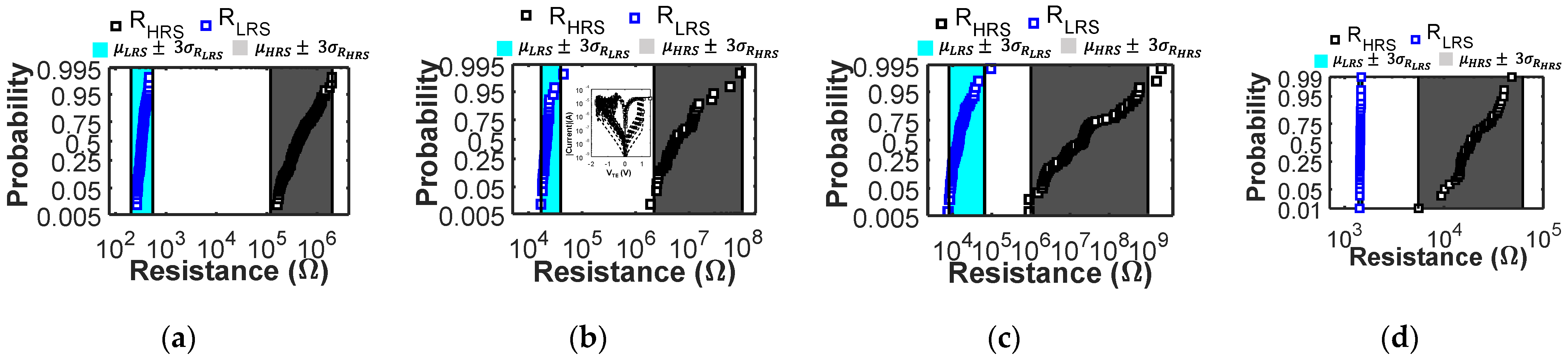
Figure 2.
Probability plots showing the experimental (cyan and grey bands) and simulated (blue and black squares) cycle to cycle variability. Cyan and grey areas indicate the range of the experimental LRS and HRS distributions. For each technology, the simulations replicate the available experimental conditions, and the reset and set voltages are reported. Specifically, (a) reports the variability obtained with technology 1 under quasi-static DC conditions (simulation variability parameters σx = 0.35 nm, σS = 2.7 nm2). Data from [26]; (b) reports the variability obtained with technology 2 under quasi-static DC conditions and IC = 20 µA, as for this technology experimental variability data [28] are available only at IC = 20 µA (variability parameters σx = 0.8 nm, σS = 24.9 nm2). The inset shows the experimental (square symbols) and simulated (lines) DC IV curves, where only kcf (kcf 20µA = kcf 200µA/100), kex (kex 20µA = kex 200µA/10), and S (S20µA = S200µA/10) parameters were changed to account for the different characteristic of the very narrow CF obtained with such low current compliance; (c) reports the variability obtained with technology 3 [29] under quasi-static DC conditions (variability parameters σx = 0.81 nm, σS = 0.7785 nm2); (d) reports the variability experimentally measured on technology 4. HRS variability data are obtained using 10 µs reset voltage pulses, while LRS data with a quasi-static positive voltage ramp as this was the only way to provide an accurate current compliance with our test setup. (Variability parameters σx = 0.7 nm, σS = 0.350 nm2).

Figure 3.
(a) Schematic of the IMPLY gate. (b) Pulses applied to the top electrodes of P (VP = VCOND) and Q (VQ = VSET) to execute the IMPLY operation. (c) Pulse applied at the top electrode of P (VP = VFALSE) to perform the FALSE P operation. (d) Truth table of the IMPLY operation where the conflicting VSET and VCOND requirements for gate functionality (*) and reduced degradation (#) for the four input combinations are evidenced.

Figure 4.
(a) Schematic of the SIMPLY architecture implemented on a linear RRAM array. (b) Pulses applied to the top electrodes of P (VP) and Q (VQ) to execute the IMPLY operation in SIMPLY architecture when the comparator detects P = Q = 0 (blue lines) and in all other cases (dashed red lines). (c) Pulse applied at the top electrode of P to perform the sFALSE P operation in SIMPLY architecture when P = 0 (dashed blue lines) and P = 1 (red lines). (d) Comparator implementation from [30] that is used in this work (45 nm technology [34]—MOSFETs W/L are shown). (e) Distribution of VN (technology 3 [29]) resulting from circuit simulations including variability and RTN (50 trials) when P = Q = 0 (violet bands) and P ≠ Q (grey bands) for a the 2-SIMPLY operation at different VREAD. The read margins (RM—blue arrows) and associated threshold voltages (VTH—orange stars) for the comparator are evidenced. Black whiskers indicate the extreme points of the distributions. Red crosses indicate outliers due to RTN. VN when P = Q = 1 is always much higher than in all other cases (thus is not reported in these box plots).

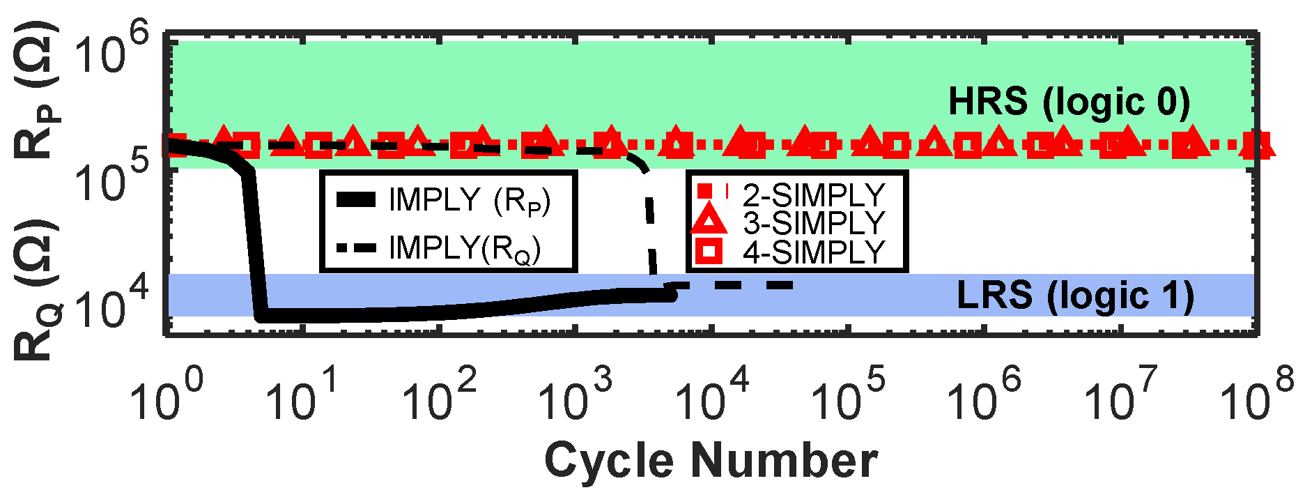
Figure 5.
Degradation profiles of RP (dashed black line) and RQ (solid black line) over time during the repeated execution of IMPLY (technology 3 [29]). RP degrades when repeating IMPLY for input combination P = Q = 0; RQ degrades when repeating IMPLY for input combination P = 1 and Q = 0. The degradation depends on the initial values of RQ and RP, (worst-cases for RQ and RP shown here, considering variability and RTN). Bit corruption occurs potentially after only 7 cycles (solid black line). No noticeable degradation occurs using SIMPLY (only worst-case reported) up to at least 108 cycles, also when performing multi-input operations (i.e., n-SIMPLY when n = 2, 3, 4—dotted red line, red triangles, and red squares, respectively).

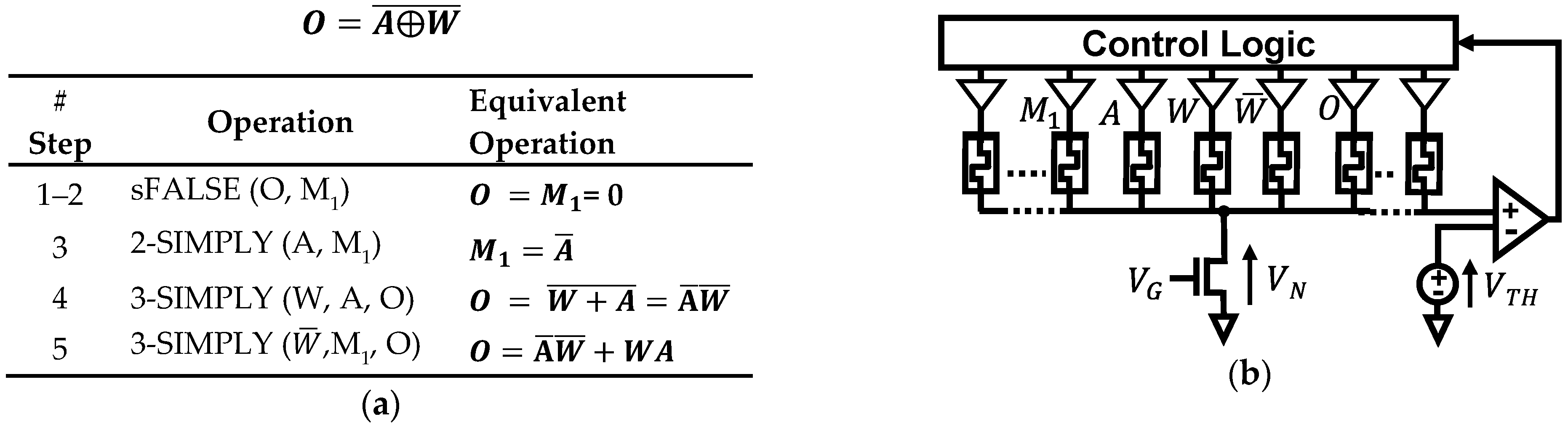
Figure 6.
SIMPLY crossbar implementation. More than one comparator can be used to increase the computation parallelism.
Figure 6.
SIMPLY crossbar implementation. More than one comparator can be used to increase the computation parallelism.

Figure 7.
Distribution of the VN voltage (a) experimentally evaluated with technology 4, and (b) simulated with the compact model calibrated on technology 3, for increasing number of input bits (i.e., n = 2, 3, 4), including variability (50 trials) when P = Q = 0 (blue bands) and P≠Q (green bands) for the n-SIMPLY operation (n = 2, 3, 4) at VREAD = 0.2 V. The read margins (RM—black arrows) and associated threshold voltages (VTH—grey circle) for the comparator are evidenced. Black whiskers indicate the extreme points of the distributions. Red crosses indicate outliers due to RTN. VN when P = Q = 1 is always much higher than in all other cases (thus is not reported in these box plots).

Figure 8.
(a) Schematic of the proposed full adder (FA). A, B, CIN are input devices (bits), X, Y, Z additional RRAMs, S and COUT output devices (bits). (b) FA total energy consumption for the 4 RRAM technologies used in this work, including variability and RTN, and considering all possible input bits’ combinations. (c) Resistance of devices A, B, CIN, S, and COUT during the FA sequence of operations (corresponding steps are reported in (d)) with A = 1, B = 0, CIN= 1 (technology 3). Input values keep unaltered. (d) List of operations required to compute the complete 1-bit full-addition.

Figure 9.
(a) Sequence of IMPLY and FALSE operations required for implementing the XNOR operation using n-SIMPLY. While 9 steps and 2 support devices are needed when using only 2-SIMPLY [30], the increased parallelism provided by n-SIMPLY reduces to 5 the number of computing steps, and only 1 support device is needed. (b) Circuit implementation of the XNOR operation on the SIMPLY architecture.

Figure 10.
n-SIMPLY-based accumulator for implementing the popcounting operation used in BNNs. (a) Two serially connected half-adders (HAs) used to implement the popcount operation. (b) Truth table of the sequence of two serially connected half-adders (HAs). The carry-out (C) of the complete operation is computed in a single step by using a 4-SIMPLY. (c) Sequence of IMPLY and FALSE operations implementing the operation described by the truth table in (b). The use of 4-SIMPLY reduces the number of computing steps from 26 (when using only the 2-SIMPLY [30]) to 19. (d) Percentage of saved computing steps for increasing number of output bits and increasing parallelism with respect to the baseline 2-SIMPLY implementation from [30]. Most computing steps are saved by using the 3-SIMPLY and up to the 4-SIMPLY operations, while further increasing the parallelism of the SIMPLY operation results in a limited improvement.

Figure 11.
Analysis of the comparator implementation for increasing n of the n-SIMPLY operation and number of compared bits. Both the total number of computing steps and the percentage of saved computing steps are reported in (a,b), respectively. The use of optimized sequences for the 3-SIMPLY (i.e., 3-SIMPLYOpt.) and 4-SIMPLY (i.e., 4-SIMPLYOpt.) operations considerably reduces the number of computing steps.


Table 1.
Energy consumption comparison of the 2-IMPLY operation in IMPLY and SIMPLY architectures with technology 3. The use of SIMPLY enables the use of a lower VSET voltage (VSET, IMPLY = 3.2 V, VSET, SIMPLY = 3 V). In all cases, 1ns voltage pulses are considered (t2-IMPLY = 2·tPULSE, t2-SIMPLY = 4·tPULSE), VREAD = 0.2 V, the effects of variability, RTN, and comparator energy overhead are included. Energy consumption data are from [30].
| Input Combination | Energy 2-IMPLY (Min–Avg–Max) | Energy 2-SIMPLY (Min–Avg–Max) | 2-SIMPLY Average Energy Improvement |
|---|---|---|---|
| P = 0 Q = 0 | 533–626–669 fJ | 498–532–557 fJ | 1.2 |
| P = 0 Q = 1 | 657–672–691 fJ | 11.7–11.8–11.9 fJ | 57 |
| P = 1 Q = 0 | 251–266–287 fJ | 11.7–11.8–11.9 fJ | 23 |
| P = 1 Q = 1 | 660–678–699 fJ | 12.6–12.6–12.6 fJ | 54 |
Table 2.
Energy consumption of FALSE operation in IMPLY and SIMPLY architectures for different RRAM technologies.
Table 2.
Energy consumption of FALSE operation in IMPLY and SIMPLY architectures for different RRAM technologies.
| Parameters | Technology 1 | Technology 2 | Technology 3 | Technology 4 |
|---|---|---|---|---|
| Energy FALSE (min-avg-max) * | 294–541–953 fJ | 160–660–1162 fJ | 90–278–492 fJ | 463–736–1471 fJ |
| Energy sFALSE (min-avg-max) * | 17–355–932 fJ | 10–406–1224 fJ | 9–175–492 fJ | 23.8–523–1446 fJ |
* The comparator overhead, variability, and RTN are included in the simulations. The average (avg) energy per operation is determined considering equiprobable initial conditions.
Table 3.
Circuit parameters and energy consumption of n-SIMPLY operation (n = 2, 3, 4) with tpulse = 1 ns.
Table 3.
Circuit parameters and energy consumption of n-SIMPLY operation (n = 2, 3, 4) with tpulse = 1 ns.
| Parameters | Tech. 1 | Tech. 2 | Tech. 3 | Tech. 4 |
|---|---|---|---|---|
| RG | 2 kΩ | 6 kΩ | 10 kΩ | 1.5 kΩ |
| VSET | 1.9 V | 1.7 V | 3 V | 1 V |
| VREAD | 0.2 V | 0.2 V | 0.2 V | 0.2 V |
| VFALSE | −1.55 V | −2 V | −2.8 V | −1.54 V |
| Energy 2-SIMPLY (min–max) * | 29 fJ–2.1 pJ | 13 fJ–370 fJ | 12 fJ–571 fJ | 35.4–462 fJ |
| Energy 3-SIMPLY (min–max) * | 30 fJ–2.2 pJ | 18 fJ–371 fJ | 13 fJ–568 fJ | 32.6–462 fJ |
| Energy 4-SIMPLY (min–max) * | 29 fJ–2.2 pJ | 12 fJ–380 fJ | 12 fJ–567 fJ | 38.7–465 fJ |
* The comparator overhead, variability, and RTN are included in the simulations by repeating the simulation 50 times for each input configuration.
Table 4.
Detailed comparison among the proposed and existing FAs in the literature. SIMPLY, IMPLY, and Hybrid-CMOS LiM solutions (both experimental and simulation works).
Table 4.
Detailed comparison among the proposed and existing FAs in the literature. SIMPLY, IMPLY, and Hybrid-CMOS LiM solutions (both experimental and simulation works).
| Author(s) | Type of Logic (exp/sim) | Physics-Based Model | # Devices | Feasible in Crossbar | Energy * (Estimated/Reported) | # Elementary Steps | Delay * (Estimated/Reported) | Retains Input Values | Endurance before Refresh ** |
|---|---|---|---|---|---|---|---|---|---|
| Siemon et al. [21] | IMPLY (sim) | YES | 8 RRAM | YES | 202 pJ (estimated) | 19 | 3.61 μs (estimated) | NO | ? |
| Lehtonen et al. [32] | IMPLY (sim) | NO | 8 RRAM | YES | - | 136 | - | YES | ? |
| Kvatinsky et al. [12] | IMPLY (sim) | NO | 9 RRAM | YES | - | 23 | 9.1 μs (estimated) | NO | ≈300 up to 105 (trades with energy) |
| Kvatinsky et al. [12] | IMPLY (sim) | NO | 6 RRAM | YES | - | 29 | 11.5 μs (estimated) | NO | ≈300 up to 105 (trades with energy) |
| Cheng et al. [36] | IMPLY (exp) | - | 8 RRAM | YES | 19.5 pJ (reported) | 27 | 54 μs (reported) | NO | ? |
| Zanotti et al. [20] | IMPLY (sim) | YES | 9 RRAM | YES | 6.4 nJ (reported) | 43 | 345 ns (reported) | YES | 67 |
| Zanotti et al. [20] | IMPLY (sim) | YES | 8 RRAM | YES | 518 pJ | 28 | 560 ns | YES | ≈ 30 |
| Zanotti et al. [20] | SIMPLY (sim) | YES | 8 RRAM | YES | 172 pJ | 28 | 920 ns (reported at 0.05GHz) | YES | >4.5·106 (no energy trade-off) |
| This Work | n-SIMPLY (sim) | YES | 8 RRAM | YES | 4.2 pJ | 11 | 42 ns | YES | >4.5·106 (no energy trade-off) |
| Junsangsri et al. [37] | CMOS LIM (sim) | YES (FET) NO (RRAM) | 41 FET + 4 RRAM | NO | 2.2 fJ (reported—excludes RRAM energy) | - | 52 ps (reported—excludes RRAM delay) | YES | ? (Limited by FET Reliability) |
* Reported means that the value was explicitly reported by the authors in the paper. Estimated means that the corresponding value has been inferred from data in the paper, although not explicitly reported by the authors. ** This information can be trusted only if a physics-based model is used.
Table 5.
Comparison between the proposed FA and a CMOS FA when executing 512 parallel 32-bit FA operations (4 kB data).
Table 5.
Comparison between the proposed FA and a CMOS FA when executing 512 parallel 32-bit FA operations (4 kB data).
| Number of Computing Devices | Energy | Delay | Energy-Delay Product (EDP) | EDP Improvement Normalized to CMOS w/VNB | |
|---|---|---|---|---|---|
| CMOS w/ VNB * | 163840–458752 FET | ≈85.5 µJ | ≈ 2.6 ms | ≈ 2.2 × 10⁻⁷ J·s | 1 |
| CMOS w/o VNB ** | 163840–458752 FET | ≈8.8 × 10⁻⁷–107 nJ | ≈ 0.2–1.2 × 10⁵ ns | ≈ 2.5 × 10⁻²⁵–1.4 × 10⁻¹¹ J·s | 1.6 × 10⁴–8.9 × 10¹⁷ |
| This Work *** | 18944 RRAM | ≈68.8 nJ | ≈1.3 µs | ≈8.9 × 10⁻¹⁴ J·s | 2.4 × 10⁶ |
| Projections IC = 10 nA f = 1 GHz **** | 18944 RRAM | ≈6.88 pJ | ≈ 0.65 µs | ≈4.5 × 10⁻¹⁸ J·s | 4.9 × 10¹⁰ |
*, **, estimates with (w/) and without (w/o) including the VNB energy and delay overhead for reading and writing 4 kB data [39]. ** CMOS FA performances were estimated projecting the time and energies for different 1-bit FA schemes and different CMOS technologies (i.e., 0.18 µm, 45 nm, and 10 nm) from [40,41,42] combined in a ripple carry configuration. ***, **** Worst-case energy estimates considering the maximum energy for each single 1-bit FA operation using Technology 3, see Figure 8b. This results in an energy overestimation that approximately accounts for additional energy overhead possibly introduced by the peripheral circuit (i.e., analog tri-state buffers contributions). **** Projections using optimized devices with IC = 10 nA [43] and f = 1 GHz [44].
Publisher’s Note: MDPI stays neutral with regard to jurisdictional claims in published maps and institutional affiliations. |
© 2021 by the authors. Licensee MDPI, Basel, Switzerland. This article is an open access article distributed under the terms and conditions of the Creative Commons Attribution (CC BY) license (https://creativecommons.org/licenses/by/4.0/).
Share and Cite
MDPI and ACS Style
Zanotti, T.; Pavan, P.; Puglisi, F.M. Multi-Input Logic-in-Memory for Ultra-Low Power Non-Von Neumann Computing. Micromachines 2021, 12, 1243. https://doi.org/10.3390/mi12101243
AMA Style
Zanotti T, Pavan P, Puglisi FM. Multi-Input Logic-in-Memory for Ultra-Low Power Non-Von Neumann Computing. Micromachines. 2021; 12(10):1243. https://doi.org/10.3390/mi12101243
Chicago/Turabian StyleZanotti, Tommaso, Paolo Pavan, and Francesco Maria Puglisi. 2021. "Multi-Input Logic-in-Memory for Ultra-Low Power Non-Von Neumann Computing" Micromachines 12, no. 10: 1243. https://doi.org/10.3390/mi12101243
Note that from the first issue of 2016, this journal uses article numbers instead of page numbers. See further details here.