
Preparation and Research of Monolayer WS2 FETs Encapsulated by h-BN Material


Key Laboratory for Wide-Band Gap Semiconductor Materials and Devices of Education, The School of Microelectronics, Xidian University, Xi’an 710071, China
*
Authors to whom correspondence should be addressed.
Micromachines 2021, 12(9), 1006; https://doi.org/10.3390/mi12091006
Submission received: 5 July 2021
/
Revised: 30 July 2021
/
Accepted: 22 August 2021
/
Published: 24 August 2021
(This article belongs to the Special Issue Electronic and Optoelectronic Devices Based on 2D Materials)
Abstract
:Functional devices that use vertical van der Waals (vdWs) heterostructure material can effectively combine the properties of single component materials, and the strong interlayer coupling effect can change their electronic and optical properties. According to our research, WS2/h-BN vertical vdWs heterostructure material can be synthesized by chemical vapor deposition (CVD) and wet transfer methods. Monolayer WS2 material and WS2/h-BN vertical vdWs heterostructure material can be tested and characterized using XPS, SEM, EDS, AFM and Raman spectroscopy, which can prove the existence of corresponding materials. When the thickness of the material decreases, the Coulomb scattering amongst two-dimensional (2D) layered materials increases. This is because both the shielding effect and the distance between the channel and the interface layer decrease. FET devices are then fabricated on WS2/h-BN vdWs heterostructure material by the electron beam lithography and evaporation processes. The effects of vdWs epitaxy on electrical transmission when WS2/h-BN vdWs heterostructure material is formed are explored. Finally, the related electrical performance of FET devices is tested and analyzed. Our experimental research provides guidance for the use of electronic devices with vdWs heterostructure material.
1. Introduction
Silicon-based transistors encounter short-channel effects and drain-induced barrier reduction problems as a device decreases in size [1,2]. To overcome these problems, atomic thickness channel material is used to eliminate the potential adverse effects of device miniaturization. Monolayer WS2 material has high mobility and a direct band gap of 2 eV, while also exhibiting valley polarization [3]. Therefore, monolayer WS2 and heterostructure materials are important for basic research and device applications, such as for photodetectors [4] and field effect transistors (FETs) [5]. The band gap of thin-layer hexagonal boron nitride (h-BN) material is 5.97 eV. The h-BN material also has a hexagonal lattice structure on the 2D plane, and the ionic bond in the layer is strong. Therefore, the chemical properties of h-BN material are stable [6,7,8]. There are no dangling bonds on the surface of h-BN material, which helps to decrease surface effects and electron scattering and improves mobility. The h-BN material is used as the encapsulation layer, which has no effect on the performance of underlying material [9]. As an excellent semiconductor material, WS2/h-BN vertical vdWs heterostructure material can be used for 2D ultra-thin electronics [10] and optoelectronic devices [11].
The preparation of WS2/h-BN vertical vdWs heterostructure material mainly includes chemical vapor deposition (CVD) preparation, i.e., mechanical peeling and transfer stacking methods [12,13]. However, the mechanical peeling and stacking method is not suitable for large-scale fabrication due to its lower yield [14]. During the transfer process, the transfer stacking method introduces impurity contamination between the h-BN and the WS2 material interfaces, which has a marked impact on the properties of WS2/h-BN heterostructure material [15]. The preparation of large-area, controllable, continuous and uniform WS2/h-BN heterostructure material is still the eminent challenge. In addition, h-BN material can be used as a packaging material, which can decrease surface chemical adsorption and the influence of the external environment on the channel material [16,17]. To improve the performance of nanodevices, different vdWs vertical heterostructure materials can be formed by h-BN, graphene and TMDs materials. Therefore, the controllable preparation of WS2/h-BN heterostructure vertical material has great significance.
Our research mainly consists of the following aspects: First, WS2, h-BN and WS2/h-BN vdWs vertical heterostructure materials are grown and prepared by CVD and wet transfer methods. Next, monolayer WS2 material is characterized by x-ray photoelectron spectroscopy (XPS), an atomic force microscope (AFM), scanning electron microscopy (SEM) and energy dispersive x-ray (EDX) spectroscopy. The Raman spectrometer is also used to test and characterize the spectral characteristics of WS2/h-BN heterostructure material in order to explore the influence of vdWs epitaxy. Subsequently, the field effect transistor (FET) based on WS2/h-BN vdWs vertical heterostructure material is prepared. Finally, the electronic transmission performance of FET devices is measured and analyzed, and the channel characteristics are enhanced by h-BN material, which is achieved by reducing external defects.
2. Materials and Methods
2.1. Preparation of WS2 Material
Monolayer WS2 material was prepared using the CVD method. During the reaction process of the WS2 material, the film quality was precisely controlled by adjusting the heating temperature, gas flow rate and reaction time [18]. This method has the advantages of large film size, high crystallinity and precise controllability. High-purity WO3 and sulfur powders were selected as the tungsten source and sulfur source, respectively. WO3 and sulfur powders (SixCarbon Technology Shenzhen, Shenzhen, China) were placed in the different reaction temperature zones of the tube furnace, and SiO2/Si substrate was placed 7 cm below the WO3 powder. To achieve the sublimation of the WO3 powder and sulfur powder, the temperature of the powders was set to 1000 °C and 200 °C, respectively. The WO3 and sulfur vapors diffused into the SiO2/Si substrate with the help of 50 sccm of Ar gas and reacted for 10 min, and thus WS2 material was obtained.
2.2. Preparation of h-BN Material
Monolayer h-BN film was grown on a copper foil substrate by a tube furnace, and the Borane Ammonia Complex was used as the growth source [19]. First, the copper foil substrate and 100 mg of borane ammonia complex were placed on the high temperature zone and the upper end of the tube furnace, respectively. The high temperature zone of the tube furnace was then heated to 1050 °C, and 10 sccm of hydrogen (H2) gas and 100 sccm of argon (Ar) gas were continuously introduced during the heating process. Next, the copper foil substrate was annealed at 1050 °C for 1 h. Immediately after, the borane ammonia complex was heated at 100 °C, which resulted in the production of nitrogen and boron. The growth time was maintained for 20 min, during which time B and N atoms combined to form h-BN material on the copper foil substrate. Finally, the copper foil with the h-BN film was removed when the high temperature zone was allowed to cool naturally.
2.3. Preparation of WS2/h-BN vdWs Vertical Heterostructure Material
To begin with, the PMMA solution was uniformly spin coated on the copper foil substrate covered with h-BN material at 500 rpm and 2500 rpm for 10 s and 20 s, respectively. Then, this copper foil substrate, spin-coated with the PMMA solution, was placed in a 120 °C oven for 3 min to cure the PMMA film, from which the PMMA/h-BN/copper foil substrate can be obtained. The PMMA/h-BN/copper foil substrate was then immersed in 1M FeCl3 solution for 1 h to corrode the copper foil and make the PMMA/h-BN film float on the surface of the solution. Next, the PMMA/h-BN film was washed with deionized water several times to remove the residual FeCl3 solution, and then the PMMA/h-BN film was placed on the WS2/SiO2/Si substrate. The PMMA/h-BN/WS2/SiO2/Si substrate was then placed at 90 °C for 1h to remove any water, which allows the PMMA/h-BN film to bond more tightly to the target substrate [20]. Finally, the PMMA layer was dissolved in a 40 °C hot acetone solution. The h-BN/WS2/SiO2/Si target substrate was rinsed with isopropanol solution and then blown dry with high-purity nitrogen (N2) gas.
2.4. Characterization Methods
The morphology, composition, layer thickness and structural properties of WS2/h-BN vdWs vertical heterostructure material can be characterized using XPS, SEM, AFM and Raman spectrometers. The Raman and PL spectra of WS2/h-BN heterostructure material were tested by Horiba LabRAM HR equipment (Jobin Yvon, France). A 532 nm laser equipped with 1800 g/mm grating can be selected in the Raman spectrometer, which can analyze the layers’ number, crystallinity and band gap [21]. The incident laser power is at 20 μW, the resolution is greater than 1 cm2/pixel and the laser spot diameter is about 1 μm. Raman and PL spectrum data were acquired and analyzed by LabSpec 5 and Origin 16 software, respectively. AFM is used to characterize the surface morphology and thickness, and can accurately identify the number of nanomaterials in the layers by combining Raman and photoluminescence spectroscopy with optical contrast [22]. The morphology and surface structure of WS2/h-BN vdWs vertical heterostructure material was characterized by SEM [23]. XPS can also be used to characterize the surface elements and chemical structure of material [24].
3. Results and Discussion
3.1. Test Characterization of WS2 Material
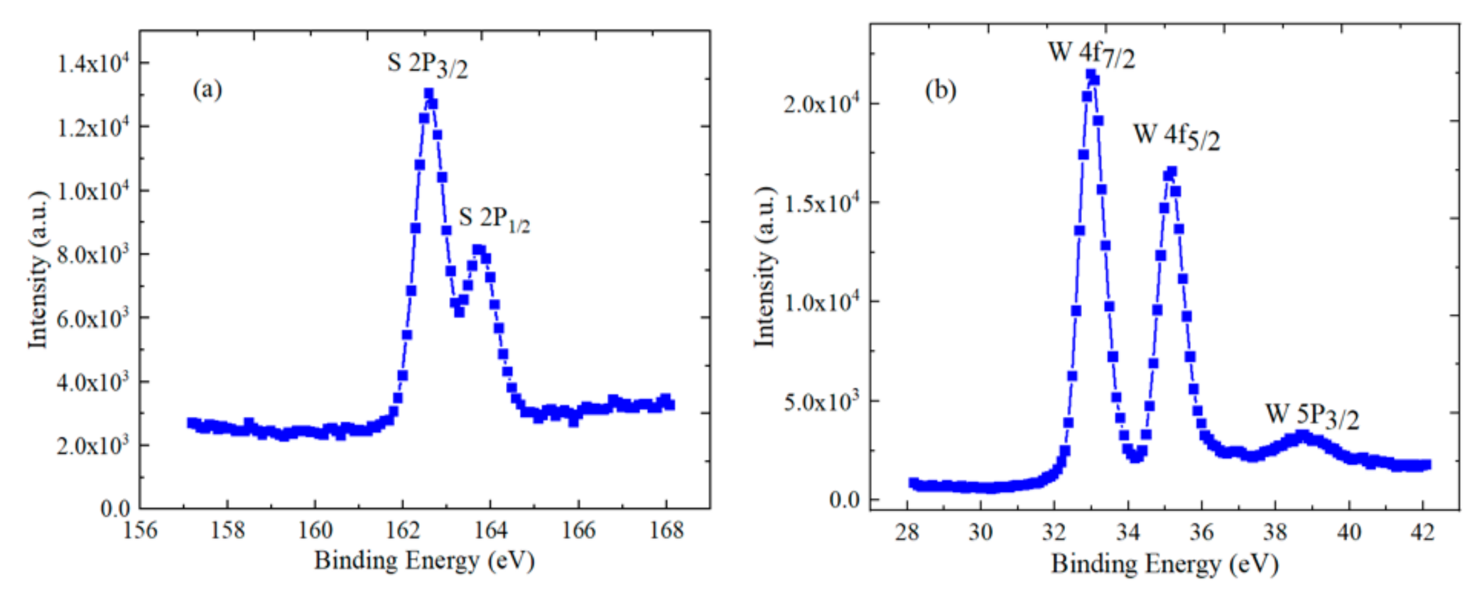
The element composition and valence state of WS2 material were analyzed by XPS, using the ESCALAB250 (Thermo Scientific Company, Waltham, MA, USA) instrument. During the process of characterization, the monochromatic Al Kα rays (1486.6 eV) were used as a radiation source, and all binding energies were measured and calibrated with the C 1s peak (284.6 eV) of carbon [25]. Observation of Figure 1a shows that 2P3/2 and 2P1/2 of S element are located at 162.57 eV and 163.67 eV, respectively. In Figure 1b, 4f7/2, 4f5/2 and 5P3/2 of W element are at 32.97 eV, 35.17 eV and 38.67 eV, respectively. The bond energies of W and S elements are consistent with the previous reports, which can prove the existence of WS2 material.
The backscattered and secondary electron signals can be obtained when high-energy electron beams hit the sample surface. The surface morphology of material can be mastered by the amplification and analysis of the above signals [26]. The surface and section morphology of WS2 material can be observed by SEM. Figure 2a shows that WS2 material has good film-forming properties. W and S elements do exist on SiO2/Si substrate, as shown in Figure 2b, where the composition of WS2 material was characterized by an energy spectrum test.
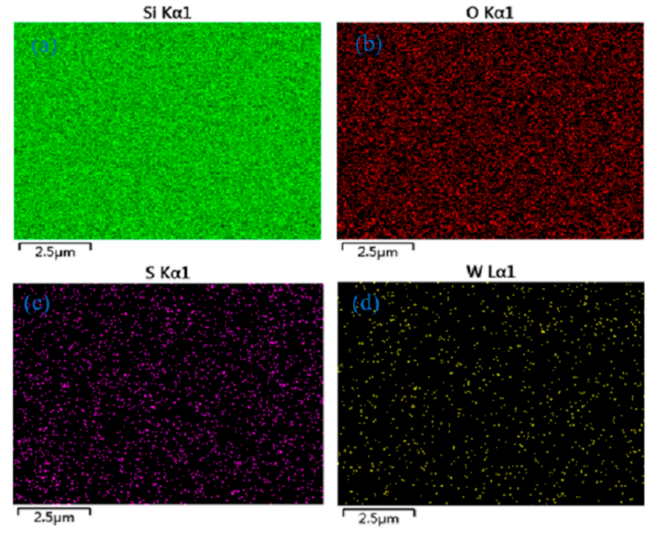
Observing Figure 3 reveals that the uniform distribution of W and S elements on the SiO2/Si substrate can be obtained by the planar EDS imaging, which further proves the existence of WS2 material.
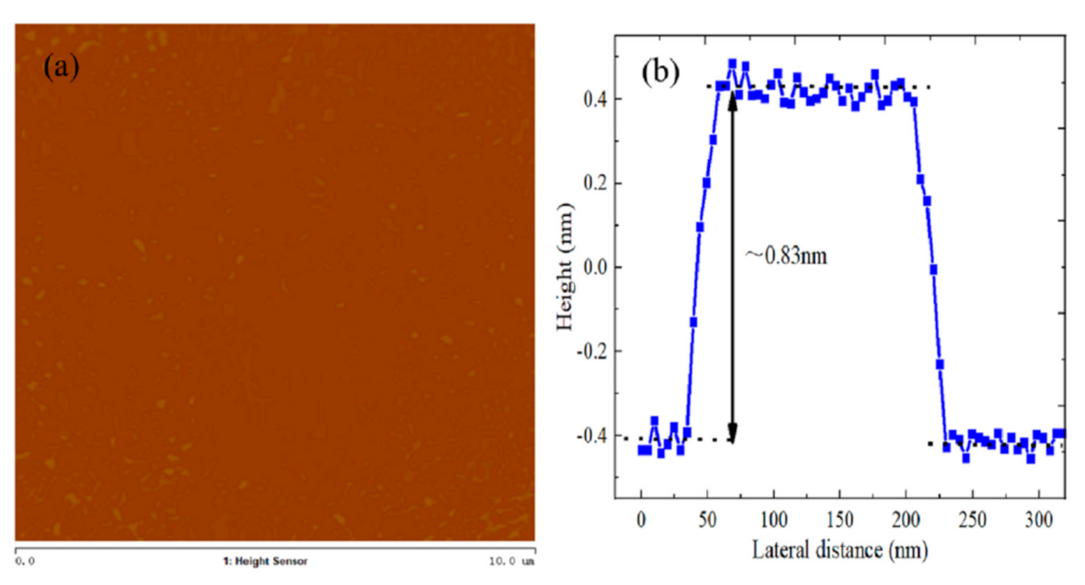
The principle behind AFM is that a micro cantilever can measure the induction of a four-quadrant detector, and the force between tiny probe tips and surface atoms can be amplified to the point of detection [27]. Therefore, the resolution of AFM can reach the atomic level. The layer number and thickness of WS2 material can be characterized and determined by AFM. In Figure 4a, WS2 material has regular morphology and a relatively flat surface, but there are also some fine particles on the surface of the film, which can be explained by the presence of a residual tungsten source. The height difference between the substrate surface and the WS2 crystal film surface is 0.83 nm, which can be considered as monolayer WS2 material, as shown in Figure 4b.
3.2. Test Characterization of WS2/h-BN Vertical Heterostructure Material
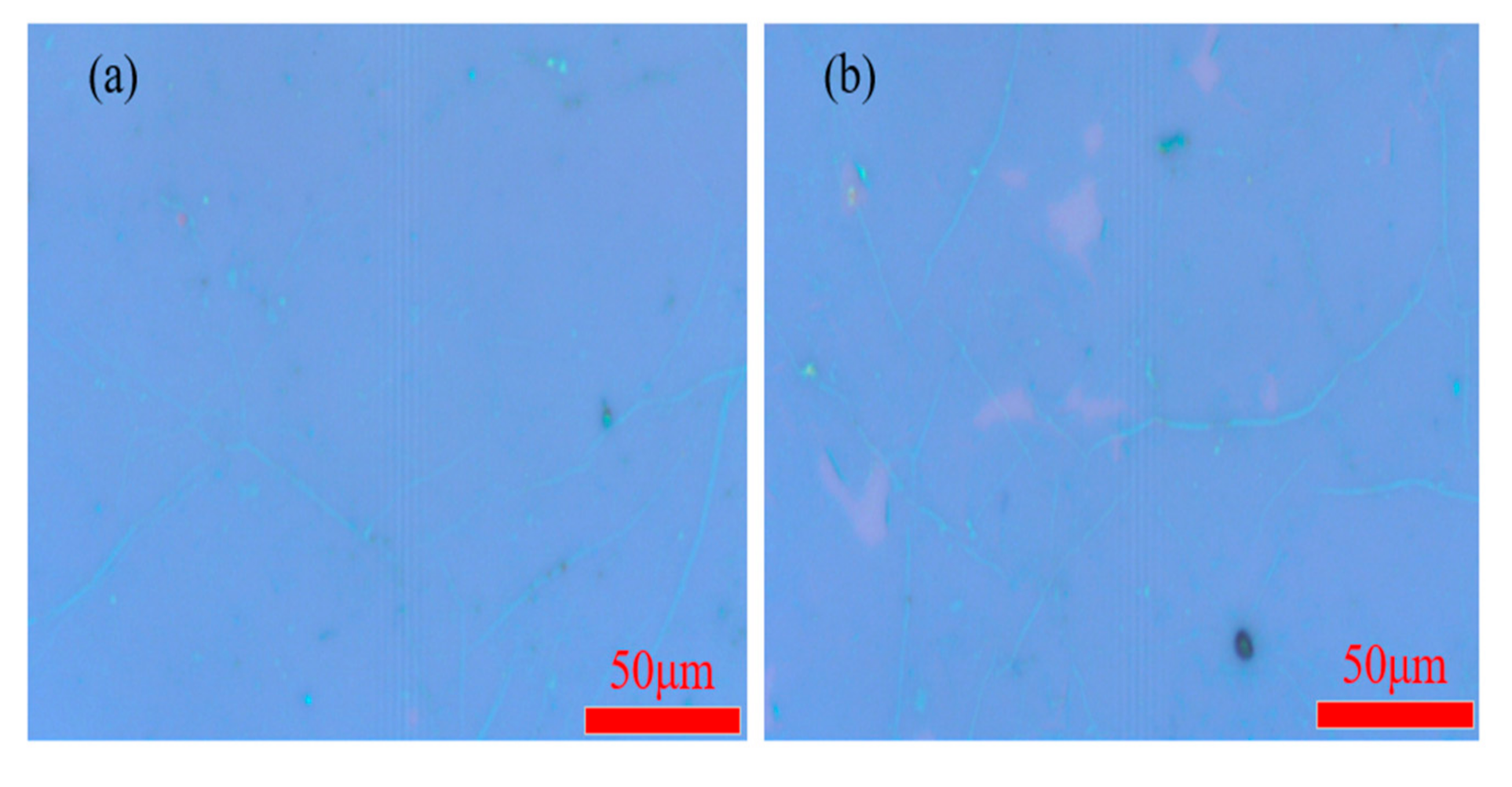
The size and morphology of layered material can be observed directly by optical microscope. Meanwhile, a simple estimate of the layer number can be achieved by the different contrast under a microscope. The morphology of WS2/h-BN vertical heterostructure material can quickly be characterized by an optical microscope. In Figure 5, WS2/h-BN vertical heterostructure material on SiO2/Si substrate has better contrast under the position 1 and position 2, and the crystallinity and thickness can further be determined by optical contrast and Raman spectroscopy.
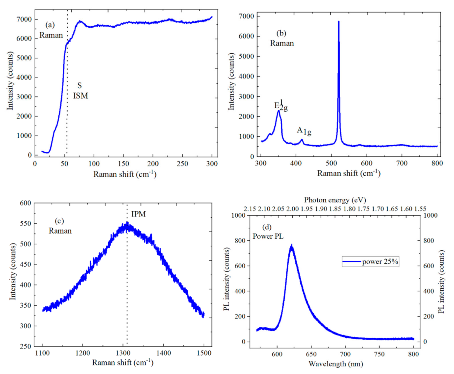
Photons excite inelastic collisions when a 532 nm laser is irradiated on the surface of a material, and this material’s information can be obtained by collecting and analyzing these photons. The 532 nm laser wavelength is used to explore the optical properties and energy band structure of WS2/h-BN vertical heterostructure material. A Raman process in h-BN material is non-resonant, which requires longer integration time and extra care. Figure 6a,c show that the ultra-low frequency and high-frequency lines are 52.5 cm−1 and 1366 cm−1 and correspond to interlayer shear mode (ISM) and in-plane mode (IPM), respectively. There is a massive difference in intensity between ISM and IPM modes, this being the sign of energy difference between the interlayer interaction and in-plane atomic interaction. The h-BN material can decrease the charge disorder and the scattering of charged impurities. In Figure 6b, the E12g in-plane vibration and A1g out-of-plane vibration modes’ characteristic peaks of monolayer WS2 material are 351.2 cm−1 and 416.2 cm−1, respectively. The frequency difference between E12g and A1g can be indicated as the layer number of 2D material, and the wavenumber difference is 65 cm−1, which is an indicator of good monolayer crystal. The intensity difference between the two vibration peaks of the monolayer WS2 material is relatively large, and the peak value of the E12g vibration mode is significantly larger than that of the A1g vibration mode. Photoluminescence (PL) spectroscopy is a non-contact and non-destructive characterization method, which is used to detect and judge the band gap between materials. The band gap changes with the layer number of the 2D material, which can determine the layer number and band gap. In Figure 6d, a 532 nm laser is used to test and characterize the WS2/h-BN vertical heterostructure material, the peak position of the strongest excitation peak is 620.9 nm, and the corresponding energy band gap is 2 eV. The intensity of the PL spectrum is related to the quality and layer number of the material, and the high luminous intensity indicates the high quality of the WS2/h-BN heterostructure material. Meanwhile, the PL spectrum of WS2 material also shows sharp exciton transition and higher PL intensity, which can be explained by the dielectric shielding effect of h-BN material. There is strain and charge rearrangement at the interface of the WS2/h-BN heterostructure material.
3.3. Preparation and Test Characterization of FET Device with WS2/h-BN Vertical Heterostructure Material
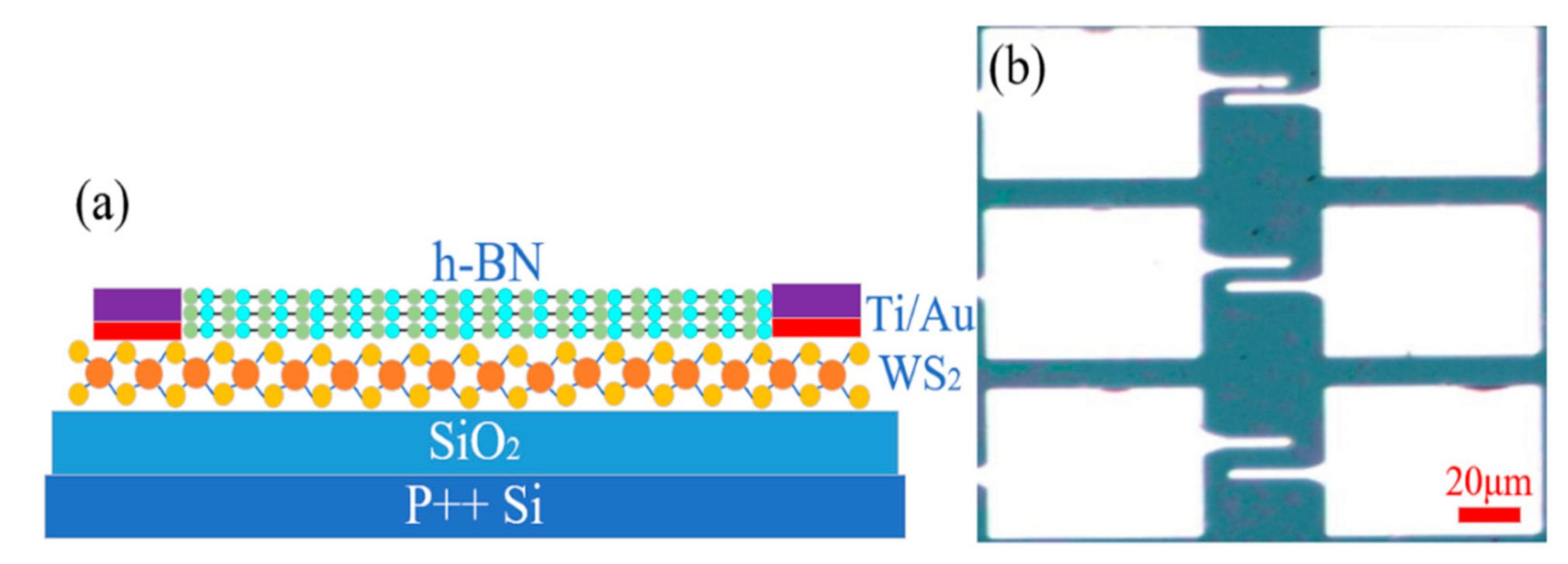
The adsorbed molecules on the surface of the semiconductor material would cause the hysteresis characteristics of 2D nano-electronic devices. Figure 7a shows the schematic diagram of the device, and h-BN material is used as an encapsulation layer to decrease the capture and release of interface charge, which can improve the electrical performance. In Figure 7b, Ti/Au (20 nm/70 nm) bimetals were deposited on WS2/h-BN vertical heterostructure material by standard electron beam lithography and electron beam evaporation processes, and the deposition rate and pressure are 1 Å/s and 10-7 Torr, respectively. Ti metal has strong adhesion to the SiO2/Si substrate, but it also causes poor semi-metal contact. The length (L) dimension of the device is 20 μm, and the width (W) dimensions are designed to be 5 μm, 10 μm and 15 μm, respectively.
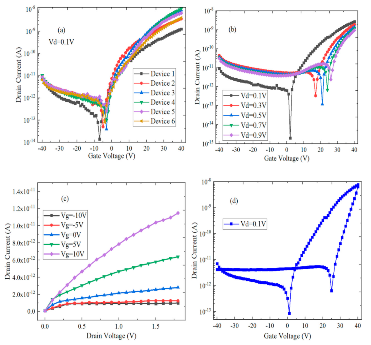
The intensity and magnitude of the current can be adjusted and controlled by the electric field effects in FET devices. Figure 8a shows the transfer characteristic curves of different FET devices with WS2/h-BN heterostructure material. As bipolar FETs, the branch current of n-type is much larger than that of p-type in the above devices. The gate voltage (Vgs) of the minimum source-drain current (Ids) value was around −5 V. Ids increases significantly by 5 orders while Vgs increases from −5 V to 40 V, which behaves like the n-type FET. When Vgs decreases from −5 V to −40 V, Ids increases monotonically, and the devices behave as p-type FET, which indicates that Fermi level can be adjusted to near valence band. On-off ratio and mobility are the main parameters by which to measure the capability of digital logic devices. The off-state leakage and on-state currents of device 3 can reach 3.9 × 10⁻¹⁴ A and 9.14 × 10⁻⁹ A when the gate voltage is selected as −3 V and 40 V, respectively. Additionally, the switching ratio is calculated to be 2.34 × 10⁵, which can implement the logic operations. The following is the calculation formula of device mobility:
In Equation (1), μ, L, W, ε0, εr and d represent the mobility, length, width, vacuum dielectric constant, relative dielectric constant of SiO2 and thickness of SiO2, respectively. The mobility of device 3 is 3.341 cm2/Vs. The transfer characteristic curves of WS2/h-BN FET under different drain voltages (Vds) are shown in Figure 8b. The gate voltage position of minimum Ids value shifts to the right as Vds increases, off-state current increases, and the corresponding switching ratio decreases. Figure 8c shows the output characteristic curves of WS2/h-BN FET and shows that the relationship of Ids to Vds is nonlinear at different Vgs. The larger Schottky barrier and contact resistance exist between WS2/h-BN heterostructure material and the Ti/Au metal electrode interface. It can be found by comparing the transfer characteristic and the output characteristic curves of WS2/h-BN FET, where the Ids of the output characteristic curve is much smaller than that of the transfer characteristic curve, which is caused by the hysteresis characteristics of the FET device. The transfer characteristic curve of WS2/h-BN FET is shown in Figure 8d, where the obvious hysteresis phenomenon exists within the atmospheric environment. The specific measurement method is that Vds is set to 0.1 V, Vgs is first scanned forward from −40 V to 40 V and then Vgs is scanned backward from 40 V to −40 V. The device behaves as the bipolar FET when Vgs scanning is in the forward direction, the minimum Ids value is located at Vgs = 1 V and the P-type branch current is very small. When Vgs scanning is in the reverse direction, the minimum Ids value is at Vgs = 25 V and the voltage offset value is 24 V. Meanwhile, in the branch where Vgs is greater than 0 V, threshold voltage shifts to the right and Ids increases significantly during reverse scanning. This is because the charge capture and release process and the scattering of charged impurities can be significantly decreased by h-BN material [28].
4. Conclusions
In this paper, WS2/h-BN vdWs vertical heterostructure material was prepared using the CVD and wet transfer methods. Raman spectrometer, AFM, SEM, XPS and EDX were used to test and characterize WS2/h-BN vdWs vertical heterostructure material. Meanwhile, FET devices were fabricated on WS2/h-BN vdWs vertical heterostructure material by standard electron beam lithography and electron beam evaporation processes, and the electrical performance of FETs was also tested and analyzed. High-quality h-BN material can effectively decrease the charge capture and release process between WS2 material and gate oxide dielectric, and the scattering of charged impurities is also significantly reduced. The switching ratio of the WS2/h-BN FET device can reach 105, and the mobility is 3.341 cm2/Vs, which meets the basic requirements of logic operations. Therefore, our research provides guidance and assistance in the application of vertical heterostructure material within the fields of electronics and optoelectronics.
Author Contributions
Conceptualization, T.H. and S.C.; methodology, S.W.; validation, K.Y.; writing—original draft preparation, T.H.; writing—review and editing, H.L.; funding acquisition, H.L. All authors have read and agreed to the published version of the manuscript.
Funding
This research was funded by the National Natural Science Foundation of China (Grant No. U1866212 and 61904136), the Fundamental Research Funds for the Central Universities (Grant No. XJS211109) and the Laboratory Open Fund of Beijing Smart-chip Microelectronics Technology Co., Ltd. The results of this paper were also supported by the China Scholarship Council (CSC No. 202006960029).
Conflicts of Interest
The authors declare no conflict of interest.
References
- Xu, W.; Kozawa, D.; Liu, Y.; Sheng, Y.; Wei, K.; Koman, V.B.; Wang, S.S.; Wang, X.C.; Jiang, T.; Strano, M.S.; et al. Determining the optimized interlayer separation distance in vertical stacked 2D WS2:hBN:MoS2 heterostructures for exciton energy transfer. Small 2018, 14, 1703727. [Google Scholar] [CrossRef]
- Ding, L.; Ukhtary, M.S.; Chubarov, M.; Choudhury, T.H.; Zhang, F.; Yang, R.; Zhang, A.; Fan, J.A.; Terrones, M.; Redwing, J.M.; et al. Understanding interlayer coupling in TMD-HBN heterostructure by Raman spectroscopy. IEEE Trans. Electron. Devices 2018, 65, 4059–4067. [Google Scholar] [CrossRef]
- Amani, M.; Chin, M.L.; Birdwell, A.G.; O’Regan, T.P.; Najmaei, S.; Liu, Z.; Ajayan, P.M.; Lou, J.; Dubey, M. Electrical performance of monolayer MoS2 field-effect transistors prepared by chemical vapor deposition. Appl. Phys. Lett. 2013, 102, 193107. [Google Scholar] [CrossRef] [Green Version]
- Hoshi, Y.; Kuroda, T.; Okada, M.; Moriya, R.; Masubuchi, S.; Watanabe, K.; Taniguchi, T.; Kitaura, R.; Machida, T. Suppression of exciton-exciton annihilation in tungsten disulfide monolayers encapsulated by hexagonal boron nitrides. Phys. Rev. B 2017, 95, 241403. [Google Scholar] [CrossRef] [Green Version]
- Xu, W.; Kozawa, D.; Zhou, Y.; Wang, Y.; Sheng, Y.; Jiang, T.; Strano, M.S.; Warner, J.H. Controlling Photoluminescence Enhancement and Energy Transfer in WS2:hBN:WS2 Vertical Stacks by Precis Interlayer Distances. Small 2020, 16, 1905985. [Google Scholar] [CrossRef] [PubMed]
- Saito, Y.; Kondo, T.; Ito, H.; Okada, M.; Shimizu, T.; Toshitaka, K.U.B.O.; Kitaura, R. Low frequency Raman study of interlayer couplings inWS2-MoS2 van derWaals heterostructures. Jpn. J. Appl. Phys. 2020, 59, 062004. [Google Scholar] [CrossRef]
- Han, T.; Liu, H.; Chen, S.; Chen, Y.; Wang, S.; Li, Z. Fabrication and Characterization of MoS2/h-BN and WS2/h-BN Heterostructures. Micromachines 2020, 11, 1114. [Google Scholar] [CrossRef] [PubMed]
- Zollner, K.; Junior, P.E.F.; Fabian, J. Giant proximity exchange and valley splitting in transition metal dichalcogenide/h-BN/(Co, Ni) heterostructures. Phys. Rev. B 2020, 101, 085112. [Google Scholar] [CrossRef] [Green Version]
- Okada, M.; Kutana, A.; Kureishi, Y.; Kobayashi, Y.; Saito, Y.; Saito, T.; Watanabe, K.; Taniguchi, T.; Gupta, S.; Miyata, Y.; et al. Direct and indirect interlayer excitons in a van der Waals heterostructure of hBN/WS2/MoS2/hBN. ACS Nano 2018, 12, 2498–2505. [Google Scholar] [CrossRef]
- Esqueda, I.S.; Tian, H.; Yan, X.; Wang, H. Transport properties and device prospects of ultrathin black phosphorus on hexagonal boron nitride. IEEE Trans. Electron. Devices 2017, 64, 5163–5171. [Google Scholar] [CrossRef]
- Zhang, F.; Wang, Y.; Erb, C.; Wang, K.; Moradifar, P.; Crespi, V.H.; Alem, N. Full orientation control of epitaxial MoS2 on hBN assisted by substrate defects. Phys. Rev. B 2019, 99, 155430. [Google Scholar] [CrossRef] [Green Version]
- Behura, S.; Nguyen, P.; Che, S.; Debbarma, R.; Berry, V. Large-area, transfer-free, oxide-assisted synthesis of hexagonal boron nitride films and their heterostructures with MoS2 and WS2. J. Am. Chem. Soc. 2015, 137, 13060–13065. [Google Scholar] [CrossRef]
- Athreya, N.; Leburton, J.P. Electronic Detection of Nucleotides in Multi-Layered MoS2-hBN Nanopore FET Devices. Biophys. J. 2020, 118, 157a. [Google Scholar] [CrossRef]
- Yang, H.; Gao, F.; Dai, M.; Jia, D.; Zhou, Y.; Hu, P. Recent advances in preparation, properties and device applications of two-dimensional h-BN and its vertical heterostructures. J. Semicond. 2017, 38, 031004. [Google Scholar] [CrossRef]
- Ahmed, T.; Bellare, P.; Debnath, R.; Roy, A.; Ravishankar, N.; Ghosh, A. Thermal History-Dependent Current Relaxation in hBN/MoS2 van derWaals Dimers. ACS Nano 2020, 14, 5909–5916. [Google Scholar] [CrossRef] [PubMed]
- Datye, I.M.; Gabourie, A.J.; English, C.D.; Smithe, K.K.; McClellan, C.J.; Wang, N.C.; Pop, E. Reduction of hysteresis in MoS2 transistors using pulsed voltage measurements. 2D Mater. 2018, 6, 011004. [Google Scholar] [CrossRef]
- Wang, S.; Wang, X.; Warner, J.H. All chemical vapor deposition growth of MoS2: H-BN vertical van der Waals heterostructures. ACS Nano 2015, 9, 5246–5254. [Google Scholar] [CrossRef] [PubMed]
- Han, T.; Liu, H.; Wang, S.; Chen, S.; Xie, H.; Yang, K. Probing the Field-Effect Transistor with Monolayer MoS2 Prepared by APCVD. Nanomaterials 2019, 9, 1209. [Google Scholar] [CrossRef] [PubMed] [Green Version]
- Li, Y.; Ye, F.; Xu, J.; Zhang, W.; Feng, P.X.L.; Zhang, X. Gate-Tuned Temperature in a Hexagonal Boron Nitride-Encapsulated 2-D Semiconductor Device. IEEE Trans. Electron. Devices 2018, 65, 4068–4072. [Google Scholar] [CrossRef]
- Okada, M.; Sawazaki, T.; Watanabe, K.; Taniguch, T.; Hibino, H.; Shinohara, H.; Kitaura, R. Direct chemical vapor deposition growth of WS2 atomic layers on hexagonal boron nitride. ACS Nano 2014, 8, 8273–8277. [Google Scholar] [CrossRef]
- Lin, M.-W.; Kravchenko, I.; Fowlkes, J.; Li, X.; Puretzky, A.; Rouleau, C.M.; Geohegan, D.B.; Xiao, K. Thickness-dependent charge transport in few-layer MoS2 field-effect transistors. Nanotechnology 2016, 27, 165203. [Google Scholar] [CrossRef] [PubMed]
- Zhu, H.; Wang, X.; Zhang, T.-B.; Yang, W.; Chen, L.; Sun, Q.-Q.; Zhang, D.W. Improved integration of ultra-thin high-k dielectrics in few-layer MoS2 FET by remote forming gas plasma pretreatment. Appl. Phys. Lett. 2017, 110, 053110. [Google Scholar]
- Liu, H.; Neal, A.T.; Ye, P.D. Channel Length Scaling of MoS2 MOSFETs. ACS Nano 2012, 6, 8563–8569. [Google Scholar] [CrossRef] [PubMed] [Green Version]
- Wang, J.; Yao, Q.; Huang, C.-W.; Zou, X.; Liao, L.; Chen, S.; Fan, Z.; Zhang, K.; Wu, W.; Xiao, X.; et al. High Mobility MoS2 Transistor with Low Schottky Barrier Contact by Using Atomic Thick h-BN as a Tunneling Layer. Adv. Mater. 2016, 28, 8302–8308. [Google Scholar] [CrossRef]
- Di Bartolomeo, A.; Genovese, L.; Foller, T.; Giubileo, F.; Luongo, G.; Croin, L.; Liang, S.-J.; Ang, L.K.; Schleberger, M. Electrical transport and persistent photoconductivity in monolayer MoS2 phototransistors. Nanotechnology 2017, 28, 214002. [Google Scholar] [CrossRef] [Green Version]
- Chow, P.K.; Singh, E.; Viana, B.C.; Gao, J.; Luo, J.; Li, J.; Lin, Z.; Elías, A.L.; Shi, Y.; Wang, Z. Wetting of mono and few-layered WS2 and MoS2 films supported on Si/SiO2 substrates. ACS Nano 2015, 9, 3023–3031. [Google Scholar] [CrossRef] [PubMed]
- Yu, F.; Liu, Q.; Gan, X.; Hu, M.; Zhang, T.; Li, C.; Kang, F.; Terrones, M.; Lv, R. Ultrasensitive Pressure Detection of Few-Layer MoS2. Adv. Mater. 2017, 29, 1603266. [Google Scholar] [CrossRef]
- Knobloch, T.; Illarionov, Y.Y.; Ducry, F.; Schleich, C.; Wachter, S.; Müller, T.; Waltl, M.; Lanza, M.; Vexler, M.I.; Luisier, M.; et al. On the suitability of hBN as an insulator for 2D material-based ultrascaled CMOS devices. Nat. Electron 2021, 4, 98–108. [Google Scholar] [CrossRef]
Figure 1.
XPS spectra of WS2 material (a) S element, (b) W element.

Figure 2.
(a) SEM image and (b) EDX spectrum of WS2 material.

Figure 3.
EDS element imaging of WS2 material on SiO2/Si substrate. (a) Si, (b) O, (c) S, (d) W.

Figure 4.
(a) AFM image and (b) height profile of WS2 material.

Figure 5.
Optical microscope image of WS2/h-BN vertical heterostructure material. (a) position 1; (b) position 2.
Figure 5.
Optical microscope image of WS2/h-BN vertical heterostructure material. (a) position 1; (b) position 2.

Figure 6.
Spectral characteristics of WS2/h-BN heterostructure material. (a) ISM mode characteristic peak of h-BN material; (b) Raman spectrum of WS2 material; (c) IPM mode characteristic peak of h-BN material; (d) Photoluminescence (PL) spectrum of WS2/h-BN heterostructure material.
Figure 6.
Spectral characteristics of WS2/h-BN heterostructure material. (a) ISM mode characteristic peak of h-BN material; (b) Raman spectrum of WS2 material; (c) IPM mode characteristic peak of h-BN material; (d) Photoluminescence (PL) spectrum of WS2/h-BN heterostructure material.

Figure 7.
(a) Schematic diagram and (b) optical microscope image of FET array devices with WS2/h-BN vertical heterostructure material.
Figure 7.
(a) Schematic diagram and (b) optical microscope image of FET array devices with WS2/h-BN vertical heterostructure material.

Figure 8.
Electrical performance test of WS2/h-BN FET device. (a) Transmission characteristic curves (Id-Vg) of different devices; (b) Transmission characteristic curves (Id-Vg) under different drain voltages (Vd); (c) The output characteristic curve (Id-Vd) under different gate voltages (Vg); (d) Bidirectional transmission characteristic curve.

Publisher’s Note: MDPI stays neutral with regard to jurisdictional claims in published maps and institutional affiliations. |
© 2021 by the authors. Licensee MDPI, Basel, Switzerland. This article is an open access article distributed under the terms and conditions of the Creative Commons Attribution (CC BY) license (https://creativecommons.org/licenses/by/4.0/).
Share and Cite
MDPI and ACS Style
Han, T.; Liu, H.; Chen, S.; Wang, S.; Yang, K. Preparation and Research of Monolayer WS2 FETs Encapsulated by h-BN Material. Micromachines 2021, 12, 1006. https://doi.org/10.3390/mi12091006
AMA Style
Han T, Liu H, Chen S, Wang S, Yang K. Preparation and Research of Monolayer WS2 FETs Encapsulated by h-BN Material. Micromachines. 2021; 12(9):1006. https://doi.org/10.3390/mi12091006
Chicago/Turabian StyleHan, Tao, Hongxia Liu, Shupeng Chen, Shulong Wang, and Kun Yang. 2021. "Preparation and Research of Monolayer WS2 FETs Encapsulated by h-BN Material" Micromachines 12, no. 9: 1006. https://doi.org/10.3390/mi12091006
Note that from the first issue of 2016, this journal uses article numbers instead of page numbers. See further details here.