Ferroelectric Switching in Trilayer Al2O3/HfZrOx/Al2O3 Structure
by
Solyee Im
1, 
Seung-Youl Kang
1,
Yeriaron Kim
1,
Jeong Hun Kim
1,
Jong-Pil Im
1,
Sung-Min Yoon
2,
Seung Eon Moon
1 and
Jiyong Woo
1,3,* 1
ICT Creative Research Laboratory, Electronics and Telecommunications Research Institute, Daejeon 34129, Korea
2
Department of Advanced Materials Engineering for Information and Electronics, Kyung Hee University, Yongin, Gyeonggi 17104, Korea
3
School of Electronics Engineering, Kyungpook National University, Daegu 41566, Korea
*
Author to whom correspondence should be addressed.
Micromachines 2020, 11(10), 910; https://doi.org/10.3390/mi11100910
Submission received: 8 September 2020
/
Revised: 25 September 2020
/
Accepted: 29 September 2020
/
Published: 30 September 2020
(This article belongs to the Special Issue Micro/Nanoscale Semiconductor Memory Devices)
Abstract
:Since ferroelectricity has been observed in simple binary oxide material systems, it has attracted great interest in semiconductor research fields such as advanced logic transistors, non-volatile memories, and neuromorphic devices. The location in which the ferroelectric devices are implemented depends on the specific application, so the process constraints required for device fabrication may be different. In this study, we investigate the ferroelectric characteristics of Zr doped HfO2 layers treated at high temperatures. A single HfZrOx layer deposited by sputtering exhibits polarization switching after annealing at a temperature of 850 °C. However, the achieved ferroelectric properties are vulnerable to voltage stress and higher annealing temperature, resulting in switching instability. Therefore, we introduce an ultrathin 1-nm-thick Al2O3 layer at both interfaces of the HfZrOx. The trilayer Al2O3/HfZrOx/Al2O3 structure allows switching parameters such as remnant and saturation polarizations to be immune to sweeping voltage and pulse cycling. Our results reveal that the trilayer not only makes the ferroelectric phase involved in the switching free from pinning, but also preserves the phase even at high annealing temperature. Simultaneously, the ferroelectric switching can be improved by preventing leakage charge.
1. Introduction
Ferroelectricity based on spontaneous polarization of dipoles in complex ternary oxides (e.g., BaTiO3) has been widely used in various electronic and sensor applications [1]. New discoveries of doped HfO2 materials suitable for complementary metal oxide semiconductor (CMOS) processes have led to the revival of ferroelectricity in the semiconductor field [2,3,4,5,6,7]. Unlike the ternary ferroelectric materials, which require a certain thickness (~100 nm) to realize the polarization switching, the ferroelectricity can be achieved in extremely thin HfO2 layer of less than 20 nm, overcoming integration challenges in the CMOS process. Interestingly, the polarization characteristics were observed in aggressively scaled one-nanometer-thick HfO2 films [8]. The attractive ferroelectric properties have been thus widely exploited to improve the sub-threshold slope in the logic transistor due to their negative capacitance [9]. Since the two stable polarization states driven by ferroelectric domains aligned by upward or downward dipoles that can be switched to each other by an electric field are shown, non-volatile memory behavior with binary information has been demonstrated. Successful memory operations have been reported experimentally in dynamic RAM [10] and even 3D vertical stacked NAND architecture [11,12]. In addition, many studies have been attempted to precisely control the number of rotated ferroelectric domains to achieve intermediate polarization states for neuromorphic analog synaptic devices [13,14].
To date, optimal dopants for the HfO2 material have been studied through material screening by examining the microstructure relevant to the crystallography of the HfO2 [15]. Among the dopants such as Si and Al [16,17,18], Zr, which is almost similar to the physical properties of the Hf element, has been representatively used. It has been believed that the observation of the ferroelectricity in hafnia films were contributed by a formation of a non-centrosymmetric Pca21 orthorhombic phase [19,20]. The ferroelectricity was also observed in the undoped HfO2 film [21], but incorporating the optimized dopants seems to make the phase transformation more effective and easier.
In addition to the physical investigations to identify root causes [22,23,24], advanced fabrication processes should be explored and developed. The ferroelectric layers have typically been grown so far with the atomic layer deposition (ALD) technique, which allows sophisticated composition control. However, as an alternative, the sputtering process to deposit the doped HfO2 not only allows the polarization switching to be observed, but also enables a cost-effective process that significantly reduces the deposition time compared to the ALD [25,26,27]. In general, the ferroelectricity is shown in the HfZrOx (HZO) materials after annealing at high temperatures that drive phase transformation into the orthorhombic crystalline phase. Note that the fabrication constraints of the ferroelectric devices must be considered differently for each application. When the doped HfO2 is used for the memory fabricated on top of the drain of the transistor or stacked vertically in three dimensions, the annealing temperature should be limited as low as possible to avoid malfunction of the metal electrode. Considering the back-end-of-line process, utilizing pressure, which is an alternative driving force, has been considered to demonstrate ferroelectricity at relatively low annealing temperatures [27,28,29]. At a given temperature, the increased pressure can lead to transformation of the crystal structure. On the other hand, the HfO2 material can be implemented as a gate dielectric during the front-end-of-line process, where high temperature annealing is performed to activate source and drain of the transistor [30]. In the latter case, since the thermal budget can be negligible, it is more important to ensure immunity to the high temperature.
Therefore, in this work, we introduced a thin Al2O3 (AlO) layer to the HZO-based ferroelectric device systems exhibiting a trilayer AlO/HZO/AlO structure for reliable polarization operations. Compared to the properties obtained from the single HZO, we investigated what ferroelectric behaviors were affected by introducing the AlO layers.
2. Experiments
A 17-nm-thick HZO was deposited on TiN metal serving as a bottom electrode (BE) by RF sputtering from a single stoichiometric Hf0.5Zr0.5O2 target with an Ar plasma at room temperature. After a Pt was deposited by an electron beam evaporator as a top electrode (TE), annealing was performed through rapid thermal annealing at a temperature of 850 °C. The high temperature was raised up for 20 s, and the target temperature was maintained for the next 50 s during annealing. Note that the specific annealing conditions mentioned above constituted the optimum process to demonstrate the ferroelectricity of the sputtered HZO in our preliminary study. The detailed experimental results were discussed in [31]. For the trilayer system, an ultrathin 1-nm-thick AlO layer grown by ALD using a trimethylaluminum precursor was introduced at both the BE and TE interfaces. The ferroelectric devices were characterized by a Keithley 4200 with pulse measurement unit modules.
3. Results and Discussion
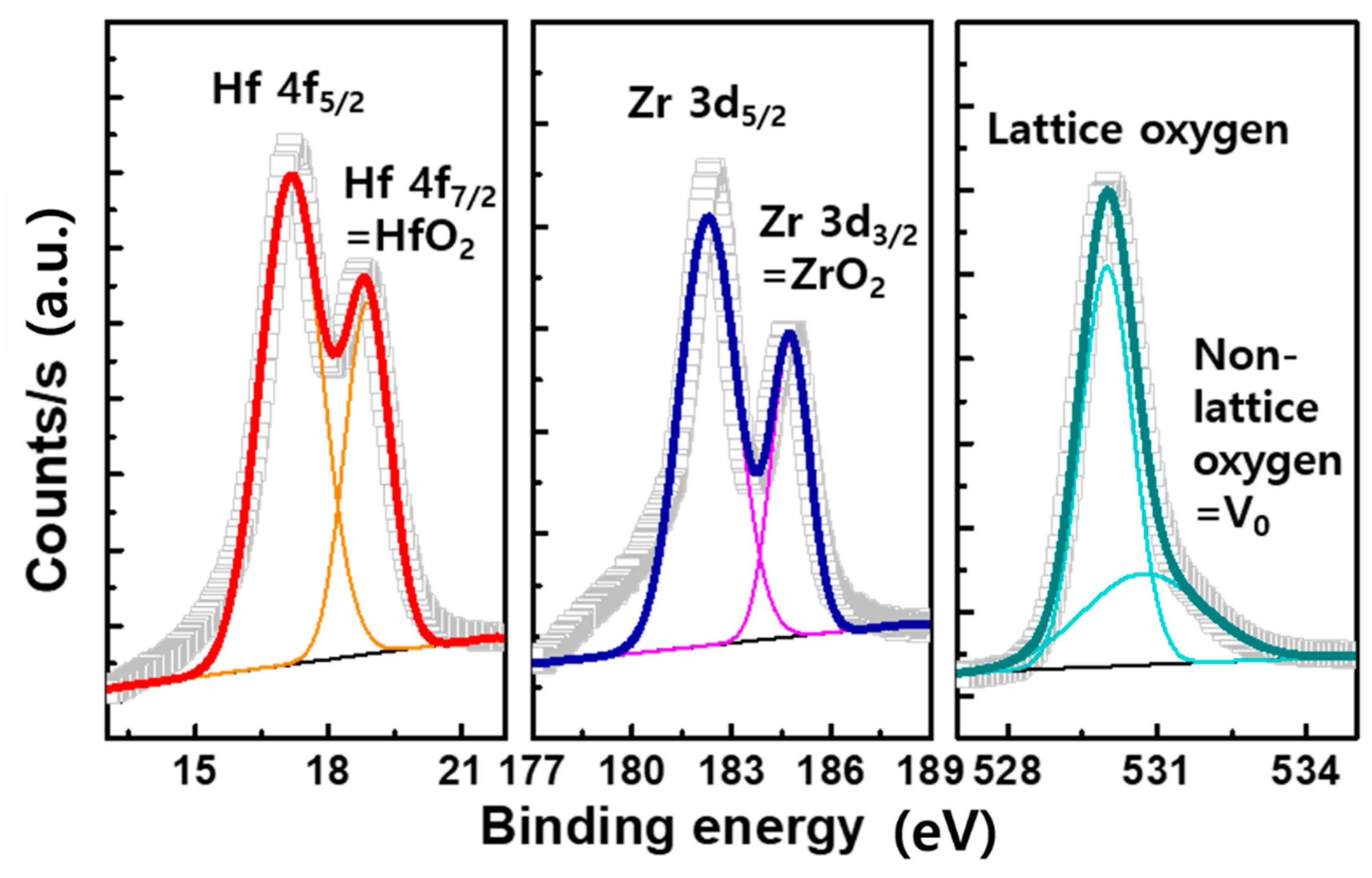
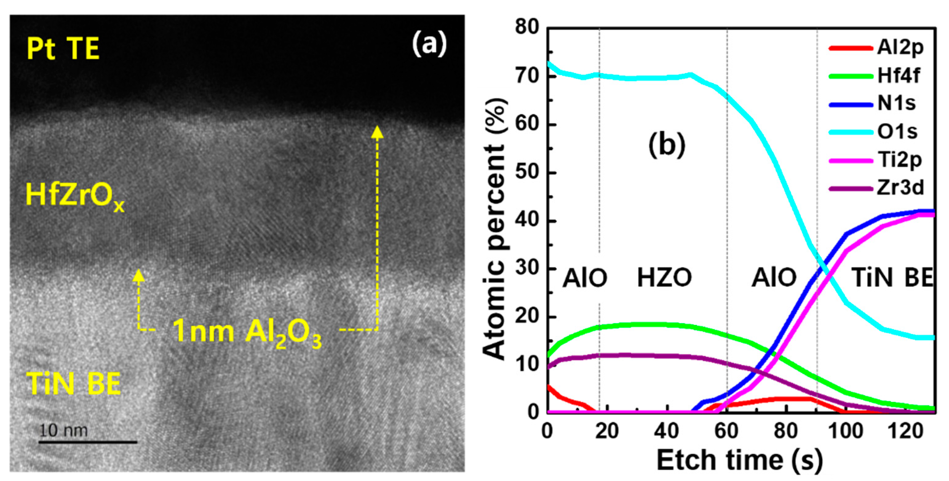
First, the physical properties of as-deposited 17-nm-thick HZO layer were analyzed. As shown in Figure 1, atomic percentages of Hf and Zr of 18 and 13 were detected via X-ray photoelectron spectroscopy, respectively. Figure 2a shows a transmission electron microscopic (TEM) image of the trilayer structure. Although the TEM analysis clearly showed crystallized HZO, it was indeed difficult to distinguish the extremely thin AlO layers at both interfaces. Instead, X-ray photoelectron spectroscopy (XPS) depth profiling indicated the presence of the AlO layers. As shown in Figure 2b, an Al 2p peak at the TE surface was increased. The peak was also observed when the Ti 2p peak representing the BE began to be detected, meaning the HZO was sandwiched by the AlO layers.
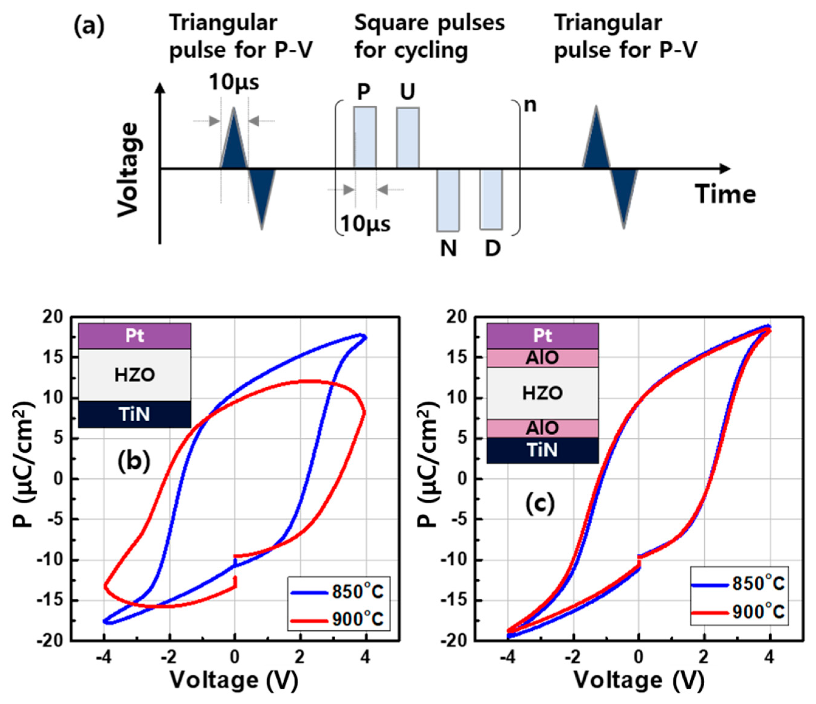
The devices were evaluated by applying a triangular pulse with a width of 10 μs corresponding to 100 kHz, as shown in Figure 3a. For a wake-up, 103 cycles of positive-up-negative-down (PUND) pulses with the same width of 10 μs were used. The subsequent square pulses were used to wake up the ferroelectric domains in the HZO and evaluate the fatigue behavior. The pulse set consisting of two consecutive positive pulses followed by two negative pulses called positive-up-negative-down technique was introduced to identify the charges solely induced by polarization [19]. Generally, charges were accumulated in the HZO capacitor not only by polarized dipoles but also by unwanted leakage instantly. By measuring the charges twice at the same state, the response from the leakage could be distinguished and excluded.
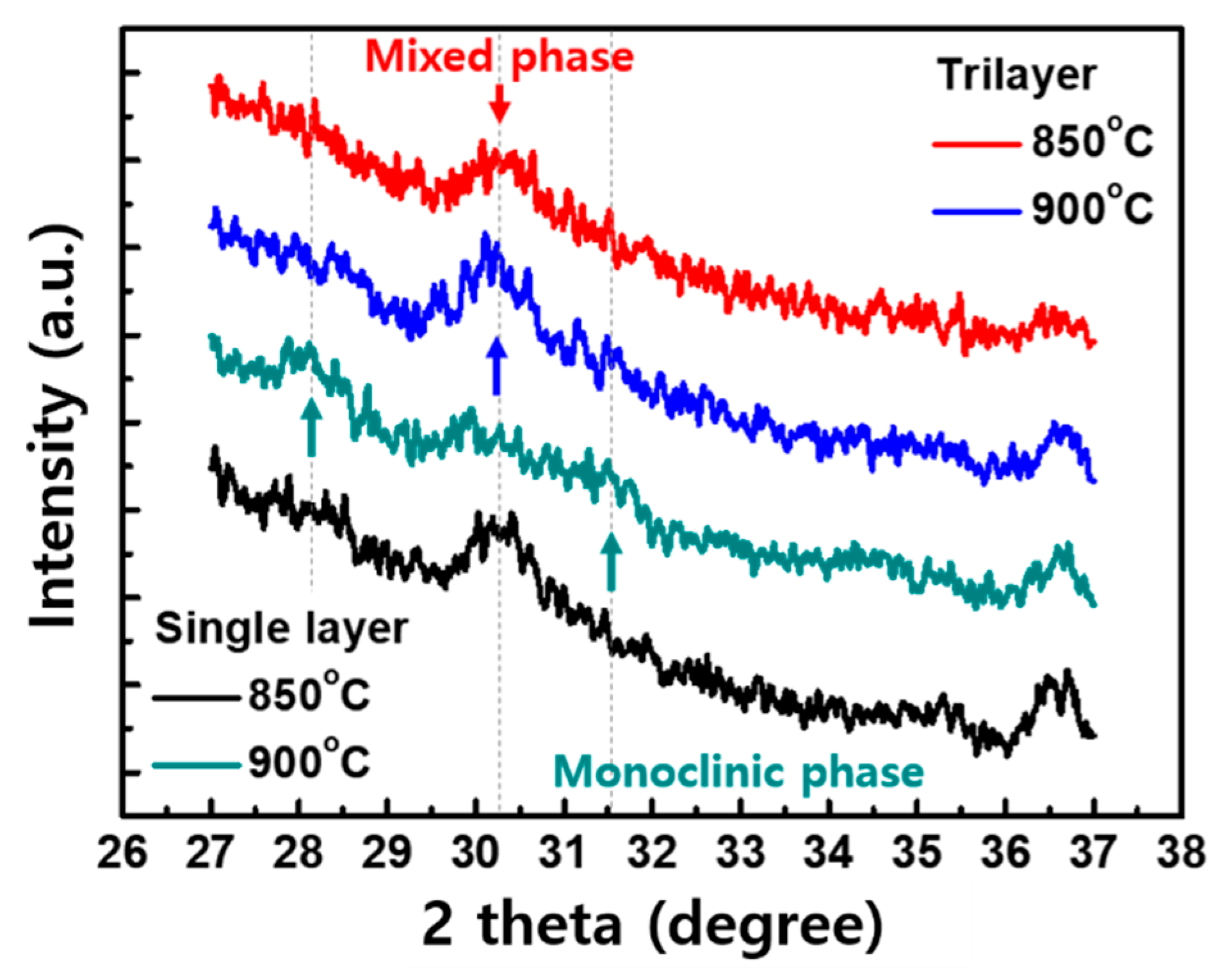
Figure 3b,c shows the polarization–voltage (P–V) curves of the devices. The pristine single layer HZO was woken-up by the PUND pulses with 2 V to prevent breakdown (Figure 3b). As the applied voltage was increased to +4 V, the polarization was rapidly transited at about +2 V, indicating a coercive voltage (Vc). A remnant polarization (Pr) at 0 V greater than 10 μC/cm2 was obtained due to spontaneously polarized dipoles in the HZO. When the single layer HZO was annealed at a slightly higher temperature of 900 °C, the P–V curve became rounded at larger voltages. On the other hand, the trilayer system showed the similar Pr compared to the single layer and was operated successfully without the breakdown by PUND pulses with a larger voltage of 4 V, as shown in Figure 3c. In addition, stable ferroelectric switching was achieved, even though the trilayer was annealed at 900 °C. These results suggest that orthorhombic phases responsible for the ferroelectricity are well preserved in the trilayer systems. As shown in Figure 4, our result showed that a noticeable peak intensity through X-ray diffraction (XRD) analysis was observed at 2 theta of about 30, indicating the mixed phase including orthorhombic, cubic, and tetragonal phases, when the polarization switching in the sputtered HZO was realized. However, the peak became lower as the annealing temperature was slightly increased. The increased other peaks adjacent the 2 theta of about 28 and 31.5 means that the monoclinic phase seemed to be transformed. It resulted in the degraded polarization behavior in the P–V trace. On the other hand, even at the high annealing temperature of 900 °C, the important mixed phase was still dominant in the trilayer, as shown in Figure 4.
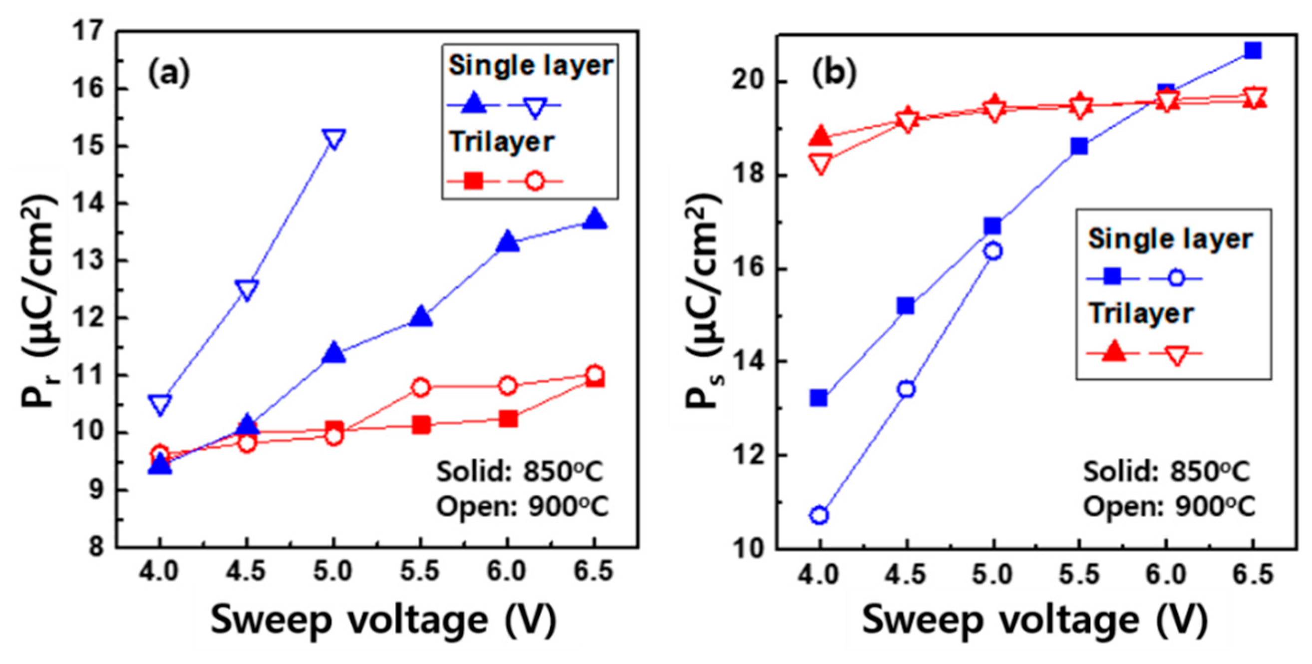
At the given wake-up cycle of 103, the Pr in the trilayer remained almost constant when sweeping the voltages larger than 6 V, no matter what annealing temperature was used, as shown in Figure 5a, whereas the Pr in the single layer was proportionally increased as a function of the voltage amplitude. Similar trends were observed not only in the Pr but also in the saturation polarization (Ps), defined as the polarization measured at 4 V, as shown in Figure 5b. The change in these parameters is related to whether the ferroelectric phases in the HZO participating in the switching are easily transformed. Basically, the deposited HZO layer is crystallized through the annealing to form the orthorhombic phases. During the phase transition, several phases are pinned by defects, resulting in the non-ferroelectric state [23]. The 103 PUND pulses were thus used to wake-up the inactivated phases. The enlarged voltage application also eliminated the defects away from the phases. These caused more phases to be involved in the ferroelectric switching. As shown in Figure 5, the parameters such as Pr and Ps in the trilayer were less sensitively affected by the electrical stimulation. This means that more active ferroelectric phases could be formed, which is in good agreement with the physical results obtained from the XRD. Meanwhile, the single layer HZO annealed at 900 °C seemed to be more vulnerable to the voltage stress, worsening the switching stability. Although the transition of the polarization at the Vc in the HZO occurred, the P–V curve was incompletely saturated in the large voltage range (Figure 3b). This was because the charges induced by the electric field were added to the Pr, which was derived by the spontaneously polarized charges. The trilayer system was able to minimize the leakage charge, resulting in the stable parameters.
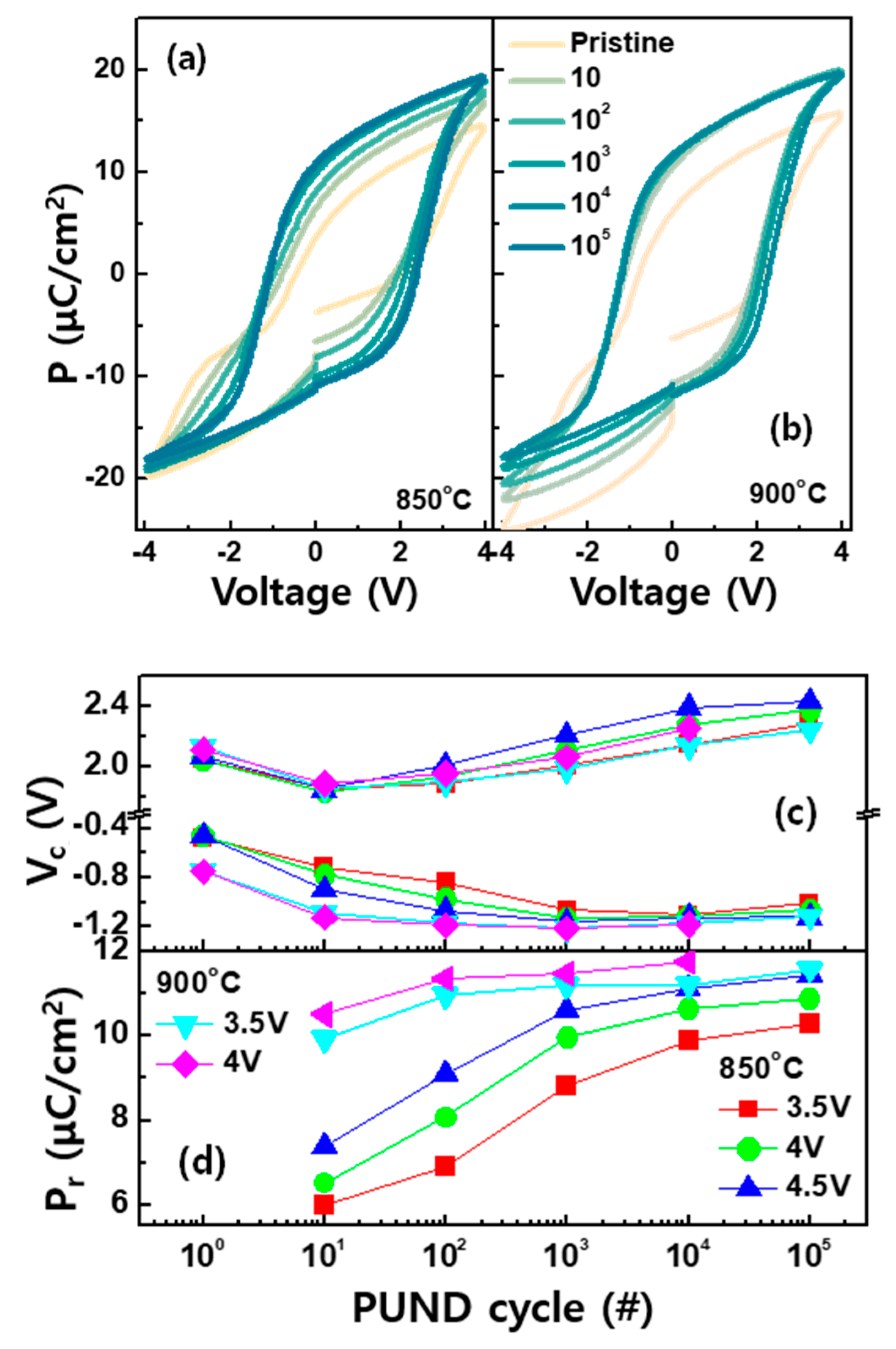
Next, we examined the P–V curves in the trilayer systems as a function of the PUND cycles to understand the impact of the annealing temperature. Figure 6a,b shows that the P–V traces after the PUND cycles with ±4 V were applied to the pristine state. Both trilayer devices initially exhibited pinched hysteresis, meaning weak antiferroelectricity [32]. As the PUND cycles were addressed to the device, the property was converted to the ferroelectricity. Note that the switching parameters such as Pr and ±Vc were more gradually changed in the device annealed at 850 °C. To achieve the Pr close to 10 μC/cm2, 103 PUND cycles were needed (Figure 6a,c). However, for the device annealed at 900 °C, only 10 cycles were required (Figure 6b,d). Unlike the single layer, where unwanted phase transformation occurred at high temperature, no distinct structural modification was observed in the trilayer (Figure 4). Rather, the high temperature seemed to be advantageous, by annihilating the pinned defects from the active ferroelectric phase. Thus, only a small amount of non-ferroelectric phases was needed to be activated, resulting in Pr quickly reaching a stable value. For the same reasons mentioned earlier, the larger PUND voltage at a given cycle accelerated the transition.
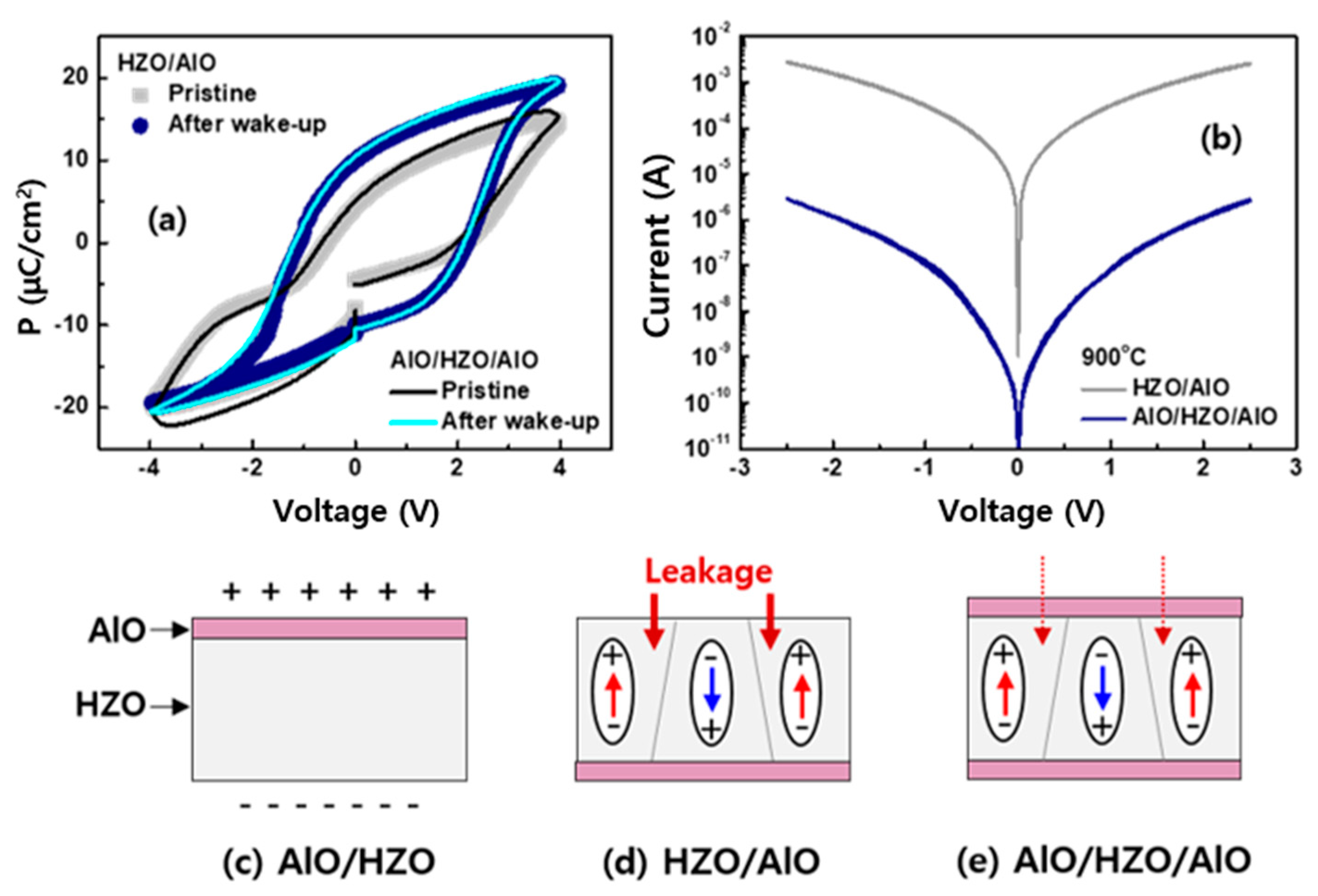
We then investigated bilayer systems annealed at 850 °C to identify the AlO layer’s role. The AlO located on top of the HZO showed a dielectric polarization temporally induced by the applied field (not shown here). When the AlO layer was inserted only between the HZO and BE, the ferroelectric switching began to be observed in Figure 7a. However, increased annealing temperature to 900 °C caused the breakdown of the bilayer HZO/AlO (from top to bottom), as we observed in the single HZO layer. The current–voltage (I–V) characteristic showed that the failure was related to the leaky HZO/AlO bilayer due to the high temperature annealing, as shown in Figure 7b. The capped AlO layer was expected to serve as a barrier to prevent additional leakage charges in the trilayer systems, as shown in Figure 7c–e. In addition, the inserted AlO layer could prevent unwanted chemical reactions between the TiN electrode and HZO during annealing [33], creating a TiOx interfacial layer with oxygen vacancies strongly affecting the ferroelectric properties of the HZO.
Similar to this work, bilayer systems with HZO/AlO ferroelectric/dielectric structures were recently reported [34,35]. Unlike the dielectric, ferroelectric (or antiferroelectric)-related layers such as ZrO2 serving as a seed layer were introduced to promote the orthorhombic phase in the doped HfO2 film [36,37]. Additional thin films have begun to be introduced rather than single HfO2, but their role and impacts on the polarization and reliability characteristics have not been elucidated. Further research to clarify these aspects is currently underway based on the fabricated multilayer ferroelectric devices. Here, we focused on the polarization behavior in a simple capacitor structure that provided a good understanding of intrinsic ferroelectric properties. When the ferroelectric switching layer was integrated into the transistor structure called ferroelectric FET (FeFET), the achieved polarization was somewhat degraded, resulting in a smaller on/off ratio for non-volatile memory applications. Thus, it remains a challenge to identify how the switching parameters such as the Pr and Vc of the ferroelectric layer are linked to reliability characteristics such as data retention and cycling endurance in the FeFET.
4. Conclusions
The recent discovery of the ferroelectricity in the doped HfO2 layer has led to great interest for next-generation non-volatile memory and neuromorphic applications. It is worth noting that the fabrication process to realize the polarization in the layer needs to be appropriately designed depending on the device configuration aimed at the target application. In this regard, we investigated the ferroelectric characteristics of the sputtered HZO film under higher temperature applications. The ferroelectric properties of the single layer HZO were vulnerable to external environments such as higher annealing temperature, causing the unwanted phase transition. The sweeping voltages accompanied by electrical stress also made the switching parameters such as Pr and Ps be disturbed by the leakage components. On the other hand, the trilayer AlO/HZO/AlO systems allowed the ferroelectric phase to be preserved even at the high annealing temperature. Rather, the temperature led the non-ferroelectric phases to be released quickly from the pinning, requiring only 10 PUND cycles for stabilization.
Author Contributions
S.I., S.-Y.K., Y.K., and J.W. performed the experiments. S.I. and J.W. characterized the fabricated devices and investigated their electrical and physical properties. J.H.K., J.-P.I., S.-M.Y., and S.E.M. discussed the experimental results. All authors have read and agreed to the published version of the manuscript.
Funding
This work was supported by a National Research Council of Science and Technology (NST) grant by the Korean government (MSIP) (No. CAP-14-01-KIST) and an Electronics and Telecommunications Research Institute (ETRI) grant funded by the Korean government (20ZB1100 and 20YB1900). This work was also supported by the National Research Foundation of Korea (NRF) grant funded by the Korea government (MSIT) (NRF-2020M3F3A2A01081775).
Conflicts of Interest
The authors declare no conflict of interest.
References
- Acosta, M.; Novak, N.; Rojas, V.; Patel, S.; Vaish, R.; Koruza, J.; Rossetti, G.A.; Rödel, J. BaTiO3-based piezoelectrics: Fundamentals, current status, and perspectives. Appl. Phys. Rev. 2017, 4, 041305. [Google Scholar] [CrossRef] [Green Version]
- Müller, J.; Yurchuk, E.; Schlosser, T.; Paul, J.; Hoffmann, R.; Muller, S.; Martin, D.; Slesazeck, S.; Polakowski, P.; Sundqvist, J.; et al. Ferroelectricity in HfO2 enables nonvolatile data storage in 28 nm HKMG. In Proceedings of the 2012 Symposium on VLSI Technology, Honolulu, HI, USA, 12–14 June 2012; pp. 25–26. [Google Scholar]
- Böscke, T.S.; Müller, J.; Bräuhaus, D.; Schröder, U.; Bottger, U. Ferroelectricity in hafnium oxide: CMOS compatible ferroelectric field effect transistors. In Proceedings of the 2011 International Electron Devices Meeting, Washington, DC, USA, 5–7 December 2011; pp. 24.5.1–24.5.4. [Google Scholar] [CrossRef]
- Park, M.H.; Lee, Y.H.; Kim, H.J.; Kim, Y.J.; Moon, T.; Kim, K.D.; Müller, J.; Kersch, A.; Schroeder, U.; Mikolajick, T.; et al. Ferroelectricity and Antiferroelectricity of Doped Thin HfO2-Based Films. Adv. Mater. 2015, 27, 1811–1831. [Google Scholar] [CrossRef]
- Batra, R.; Huan, T.D.; Jones, J.L.; Rossetti, G.A.; Ramprasad, R. Factors Favoring Ferroelectricity in Hafnia: A First-Principles Computational Study. J. Phys. Chem. C 2017, 121, 4139–4145. [Google Scholar] [CrossRef]
- Dogan, M.; Gong, N.; Ma, T.-P.; Ismail-Beigi, S. Causes of ferroelectricity in HfO2-based thin films: An ab initio perspective. Phys. Chem. Chem. Phys. 2019, 21, 12150–12162. [Google Scholar] [CrossRef] [Green Version]
- Park, M.H.; Lee, Y.H.; Mikolajick, T.; Schroeder, U.; Hwang, C.S. Review and perspective on ferroelectric HfO2-based thin films for memory applications. MRS Commun. 2018, 8, 795–808. [Google Scholar] [CrossRef] [Green Version]
- Cheema, S.S.; Kwon, D.; Shanker, N.; Dos Reis, R.; Hsu, S.-L.; Xiao, J.; Zhang, H.; Wagner, R.; Datar, A.; McCarter, M.R.; et al. Enhanced ferroelectricity in ultrathin films grown directly on silicon. Nature 2020, 580, 478–482. [Google Scholar] [CrossRef] [PubMed]
- Khan, A.I.; Yeung, C.W.; Hu, C.; Salahuddin, S. Ferroelectric negative capacitance MOSFET: Capacitance tuning & antiferroelectric operation. In Proceedings of the 2011 International Electron Devices Meeting, Washington, DC, USA, 5–7 December 2011; pp. 11.3.1–11.3.4. [Google Scholar] [CrossRef]
- Polakowski, P.; Riedel, S.; Weinreich, W.; Rudolf, M.; Sundqvist, J.; Seidel, K.; Müller, J. Ferroelectric deep trench capacitors based on Al:HfO2 for 3D nonvolatile memory applications. In Proceedings of the 2014 IEEE 6th International Memory Workshop (IMW), Taipei, Taiwan, 18–21 May 2014; pp. 1–4. [Google Scholar]
- Florent, K.; Lavizzari, S.; Di Piazza, L.; Popovici, M.; Vecchio, E.; Potoms, G.; Groeseneken, G.; Van Ihoudt, J. First demonstration of vertically stacked ferroelectric Al doped HfO2 devices for NAND applications. In Proceedings of the 2017 Symposium on VLSI Technology, Kyoto, Japan, 5–8 June 2017; pp. T158–T159. [Google Scholar]
- Florent, K.; Pesic, M.; Subirats, A.; Banerjee, K.; Lavizzari, S.; Arreghini, A.; Di Piazza, L.; Potoms, G.; Sebaai, F.; McMitchell, S.R.C.; et al. Vertical Ferroelectric HfO2 FET based on 3-D NAND Architecture: Towards Dense Low-Power Memory. In Proceedings of the 2018 IEEE International Electron Devices Meeting (IEDM), San Francisco, CA, USA, 1–5 December 2018; pp. 2.5.1–2.5.4. [Google Scholar] [CrossRef]
- Jerry, M.; Chen, P.-Y.; Zhang, J.; Sharma, P.; Ni, K.; Yu, S.; Datta, S. Ferroelectric FET analog synapse for acceleration of deep neural network training. In Proceedings of the 2017 IEEE International Electron Devices Meeting (IEDM), San Francisco, CA, USA, 2–6 December 2017; pp. 6.2.1–6.2.4. [Google Scholar] [CrossRef]
- Oh, S.; Kim, T.; Kwak, M.; Song, J.; Woo, J.; Jeon, S.; Yoo, I.K.; Hwang, H. HfZrOx-Based Ferroelectric Synapse Device With 32 Levels of Conductance States for Neuromorphic Applications. IEEE Electron Device Lett. 2017, 38, 732–735. [Google Scholar] [CrossRef]
- Chernikova, A.G.; Kuzmichev, D.; Negrov, D.V.; Kozodaev, M.; Polyakov, S.N.; Markeev, A.M. Ferroelectric properties of full plasma-enhanced ALD TiN/La:HfO2/TiN stacks. Appl. Phys. Lett. 2016, 108, 242905. [Google Scholar] [CrossRef]
- Müller, J.; Schröder, U.; Böscke, T.S.; Müller, I.; Böttger, U.; Wilde, L.; Sundqvist, J.; Lemberger, M.; Kücher, P.; Mikolajick, T.; et al. Ferroelectricity in yttrium-doped hafnium oxide. J. Appl. Phys. 2011, 110, 114113. [Google Scholar] [CrossRef]
- Mueller, S.; Mueller, J.; Singh, A.; Riedel, S.; Sundqvist, J.; Schroeder, U.; Mikolajick, T. Incipient Ferroelectricity in Al-Doped HfO2 Thin Films. Adv. Funct. Mater. 2012, 22, 2412–2417. [Google Scholar] [CrossRef]
- Park, M.H.; Schenk, T.; Fancher, C.M.; Grimley, E.D.; Zhou, C.; Richter, C.; Lebeau, J.M.; Jones, J.L.; Mikolajick, T.; Schroeder, U. A comprehensive study on the structural evolution of HfO2 thin films doped with various dopants. J. Mater. Chem. C 2017, 5, 4677–4690. [Google Scholar] [CrossRef]
- Schroeder, U.; Hwang, C.S.; Funakubo, H. Ferroelectricity in Doped Hafnium Oxide: Materials, Properties and Devices; Elsevier: Amsterdam, The Netherlands, 2019. [Google Scholar] [CrossRef]
- Müller, J.; Polakowski, P.; Mueller, S.; Mikolajick, T. Ferroelectric Hafnium Oxide Based Materials and Devices: Assessment of Current Status and Future Prospects. ECS J. Solid State Sci. Technol. 2015, 4, N30–N35. [Google Scholar] [CrossRef]
- Mittmann, T.; Materano, M.; Lomenzo, P.D.; Park, M.H.; Stolichnov, I.; Cavalieri, M.; Zhou, C.; Chung, C.; Jones, J.L.; Szyjka, T.; et al. Origin of Ferroelectric Phase in Undoped HfO2 Films Deposited by Sputtering. Adv. Mater. Interfaces 2019, 6. [Google Scholar] [CrossRef] [Green Version]
- Pesic, M.; Fengler, F.P.G.; Slesazeck, S.; Schroeder, U.; Mikolajick, T.; Larcher, L.; Padovani, A. Root cause of degradation in novel HfO2-based ferroelectric memories. In Proceedings of the 2016 IEEE International Reliability Physics Symposium (IRPS), Pasadena, CA, USA, 17–21 April 2016. [Google Scholar] [CrossRef]
- Pesic, M.; Fengler, F.P.G.; Larcher, L.; Padovani, A.; Schenk, T.; Grimley, E.D.; Sang, X.; Lebeau, J.M.; Slesazeck, S.; Schroeder, U.; et al. Physical Mechanisms behind the Field-Cycling Behavior of HfO2-Based Ferroelectric Capacitors. Adv. Funct. Mater. 2016, 26, 4601–4612. [Google Scholar] [CrossRef]
- Sang, X.; Grimley, E.D.; Schenk, T.; Schroeder, U.; Lebeau, J.M. On the structural origins of ferroelectricity in HfO2 thin films. Appl. Phys. Lett. 2015, 106, 162905. [Google Scholar] [CrossRef]
- Luo, Q.; Ma, H.; Su, H.; Xue, K.-H.; Cao, R.; Gao, Z.; Yu, J.; Gong, T.; Xu, X.; Yin, J.; et al. Composition-Dependent Ferroelectric Properties in Sputtered HfXZr1−XO2 Thin Films. IEEE Electron Device Lett. 2019, 40, 570–573. [Google Scholar] [CrossRef]
- Min, D.-H.; Kang, S.Y.; Moon, S.E.; Yoon, S.-M. Impact of Thickness Control of Hf0.5Zr0.5O2 Films for the Metal–Ferroelectric–Insulator–Semiconductor Capacitors. IEEE Electron Device Lett. 2019, 40, 1032–1035. [Google Scholar] [CrossRef]
- Woo, J.; Goh, Y.; Im, S.; Hwang, J.H.; Kim, Y.; Kim, J.H.; Im, J.-P.; Yoon, S.-M.; Moon, S.E.; Jeon, S. Improved Ferroelectric Switching in Sputtered HfZrOx Device Enabled by High Pressure Annealing. IEEE Electron Device Lett. 2020, 41, 232–235. [Google Scholar] [CrossRef]
- Goh, Y.; Jeon, S. Enhanced tunneling electroresistance effects in HfZrO-based ferroelectric tunnel junctions by high-pressure nitrogen annealing. Appl. Phys. Lett. 2018, 113, 052905. [Google Scholar] [CrossRef]
- Kim, T.; Jeon, S. Pulse Switching Study on the HfZrO Ferroelectric Films With High Pressure Annealing. IEEE Trans. Electron Devices 2018, 65, 1771–1773. [Google Scholar] [CrossRef]
- Cheng, C.-H.; Chin, A. Low-Voltage Steep Turn-On pMOSFET Using Ferroelectric High-k Gate Dielectric. IEEE Electron Device Lett. 2014, 35, 274–276. [Google Scholar] [CrossRef]
- Kim, Y.; Woo, J.; Im, S.; Lee, Y.; Kim, J.H.; Im, J.-P.; Suh, D.; Yang, S.M.; Yoon, S.-M.; Moon, S.E. Optimized annealing conditions to enhance stability of polarization in sputtered HfZrOx layers for non-volatile memory applications. Curr. Appl. Phys. 2020. accepted. [Google Scholar]
- Müller, J.; Boscke, T.S.; Schröder, U.; Mueller, S.; Bräuhaus, D.; Böttger, U.; Frey, L.; Mikolajick, T. Ferroelectricity in Simple Binary ZrO2 and HfO2. Nano Lett. 2012, 12, 4318–4323. [Google Scholar] [CrossRef] [PubMed]
- Stengel, M.; Spaldin, N.A. Origin of the dielectric dead layer in nanoscale capacitors. Nature 2006, 443, 679–682. [Google Scholar] [CrossRef] [PubMed]
- Si, M.; Lyu, X.; Ye, P.D. Ferroelectric Polarization Switching of Hafnium Zirconium Oxide in a Ferroelectric/Dielectric Stack. ACS Appl. Electron. Mater. 2019, 1, 745–751. [Google Scholar] [CrossRef] [Green Version]
- Ryu, H.; Wu, H.; Rao, F.; Zhu, W. Ferroelectric Tunneling Junctions Based on Aluminum Oxide/ Zirconium-Doped Hafnium Oxide for Neuromorphic Computing. Sci. Rep. 2019, 9, 20383. [Google Scholar] [CrossRef] [Green Version]
- Onaya, T.; Nabatame, T.; Sawamoto, N.; Ohi, A.; Ikeda, N.; Chikyow, T.; Ogura, A. Improvement in ferroelectricity of HfxZr1−xO2 thin films using ZrO2 seed layer. Appl. Phys. Express 2017, 10, 81501. [Google Scholar] [CrossRef]
- Xiao, W.; Liu, C.; Peng, Y.; Zheng, S.; Feng, Q.; Zhang, C.; Zhang, J.; Hao, Y.; Liao, M.; Zhou, Y.; et al. Performance Improvement of Hf0.5Zr0.5O2-Based Ferroelectric-Field-Effect Transistors With ZrO2 Seed Layers. IEEE Electron Device Lett. 2019, 40, 714–717. [Google Scholar] [CrossRef]
Figure 1.
The XPS of the as-deposited 17-nm-thick HZO layer.

Figure 2.
(a) Cross-sectional TEM image of the trilayer AlO/HZO/AlO structure. The crystallized phases were shown in the HZO. (b) XPS depth profile of the trilayer. The Al peaks were detected at the both interfaces.
Figure 2.
(a) Cross-sectional TEM image of the trilayer AlO/HZO/AlO structure. The crystallized phases were shown in the HZO. (b) XPS depth profile of the trilayer. The Al peaks were detected at the both interfaces.

Figure 3.
(a) The schematic illustration of each pulse for the P–V test and PUND cycling. The P–V curves after 103 PUND cycles of the (b) single layer HZO and (c) trilayer AlO/HZO/AlO. The devices were annealed via RTA at temperatures of 850 and 900 °C.
Figure 3.
(a) The schematic illustration of each pulse for the P–V test and PUND cycling. The P–V curves after 103 PUND cycles of the (b) single layer HZO and (c) trilayer AlO/HZO/AlO. The devices were annealed via RTA at temperatures of 850 and 900 °C.

Figure 4.
Highest peak intensity at 2 theta of around 30° was shown in the trilayer, whereas the peak was decreased in the single layer annealed at 900 °C.
Figure 4.
Highest peak intensity at 2 theta of around 30° was shown in the trilayer, whereas the peak was decreased in the single layer annealed at 900 °C.

Figure 5.
(a) Pr and (b) Ps measured at 0 V and 4 V, respectively, as a function of the sweep voltages. The trilayer devices exhibited stable switching parameters over the entire voltage range.
Figure 5.
(a) Pr and (b) Ps measured at 0 V and 4 V, respectively, as a function of the sweep voltages. The trilayer devices exhibited stable switching parameters over the entire voltage range.

Figure 6.
The P–V curves of the trilayer annealed at (a) 850 °C and (b) 900 °C. The extracted (c) ±Vc and (d) Pr as a function of the voltage amplitude of the PUND cycles.
Figure 6.
The P–V curves of the trilayer annealed at (a) 850 °C and (b) 900 °C. The extracted (c) ±Vc and (d) Pr as a function of the voltage amplitude of the PUND cycles.

Figure 7.
(a) The P–V curves of the device systems annealed at 850 °C. (b) I–V traces of both device systems annealed at 900 °C. The dielectric and spontaneous polarizations were shown in (c) AlO/HZO and (d) HZO/AlO structures, respectively. (e) Stable ferroelectric switching was observed in the trilayer systems annealed at the higher temperature of 900 °C.

© 2020 by the authors. Licensee MDPI, Basel, Switzerland. This article is an open access article distributed under the terms and conditions of the Creative Commons Attribution (CC BY) license (http://creativecommons.org/licenses/by/4.0/).
Share and Cite
MDPI and ACS Style
Im, S.; Kang, S.-Y.; Kim, Y.; Kim, J.H.; Im, J.-P.; Yoon, S.-M.; Moon, S.E.; Woo, J. Ferroelectric Switching in Trilayer Al2O3/HfZrOx/Al2O3 Structure. Micromachines 2020, 11, 910. https://doi.org/10.3390/mi11100910
AMA Style
Im S, Kang S-Y, Kim Y, Kim JH, Im J-P, Yoon S-M, Moon SE, Woo J. Ferroelectric Switching in Trilayer Al2O3/HfZrOx/Al2O3 Structure. Micromachines. 2020; 11(10):910. https://doi.org/10.3390/mi11100910
Chicago/Turabian StyleIm, Solyee, Seung-Youl Kang, Yeriaron Kim, Jeong Hun Kim, Jong-Pil Im, Sung-Min Yoon, Seung Eon Moon, and Jiyong Woo. 2020. "Ferroelectric Switching in Trilayer Al2O3/HfZrOx/Al2O3 Structure" Micromachines 11, no. 10: 910. https://doi.org/10.3390/mi11100910
Note that from the first issue of 2016, this journal uses article numbers instead of page numbers. See further details here.