Extrinsic and Intrinsic Frequency Dispersion of High-k Materials in Capacitance-Voltage Measurements

Abstract
:1. Introduction
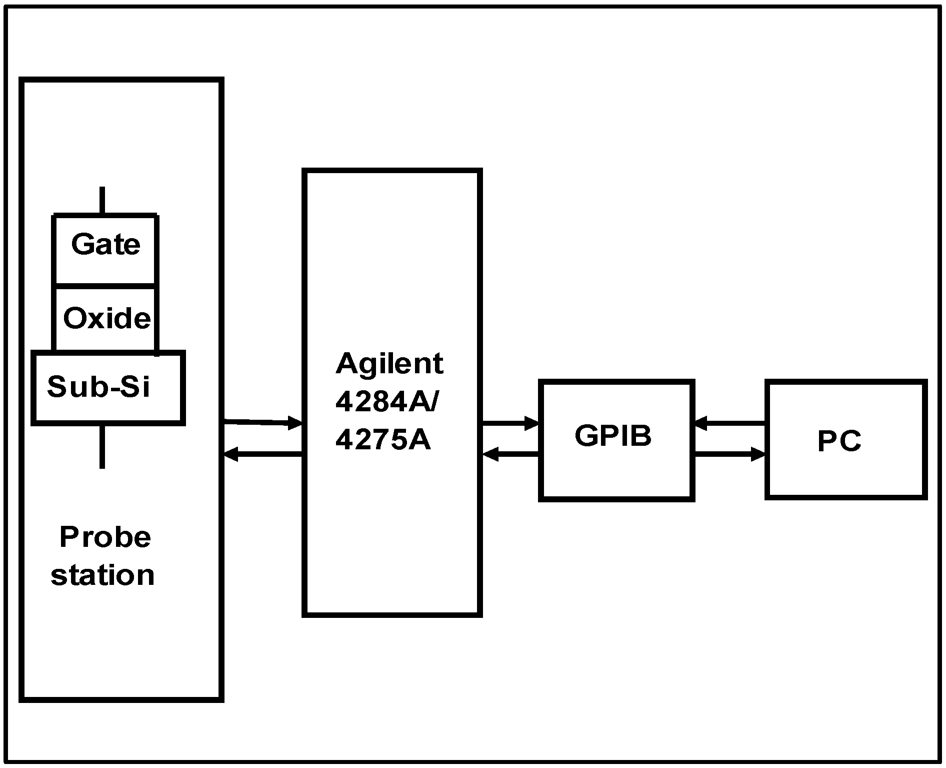
2. Experimental


3. Results and Discussion
3.1. Extrinsic Causes of Frequency Dispersion During C-V Measurement


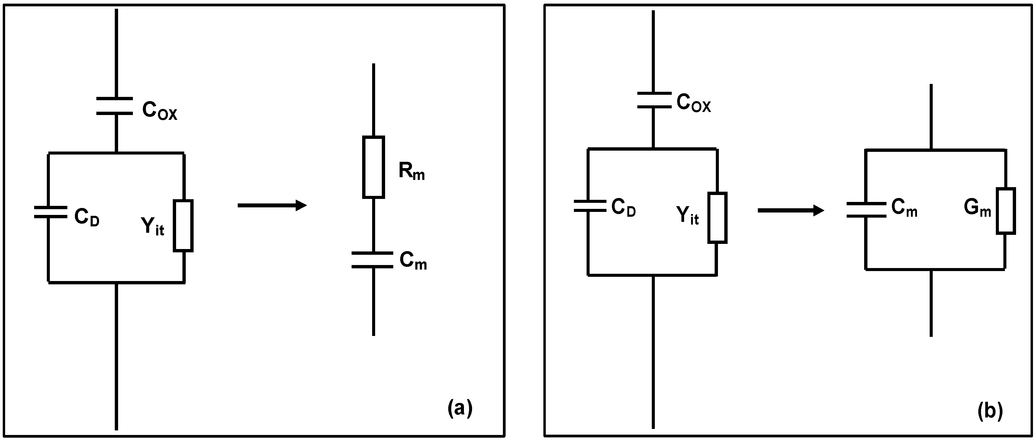
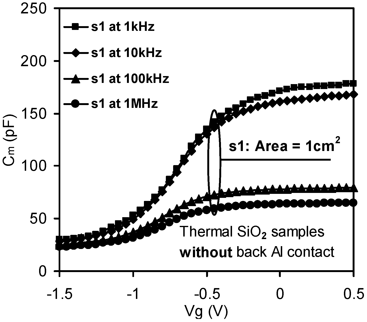
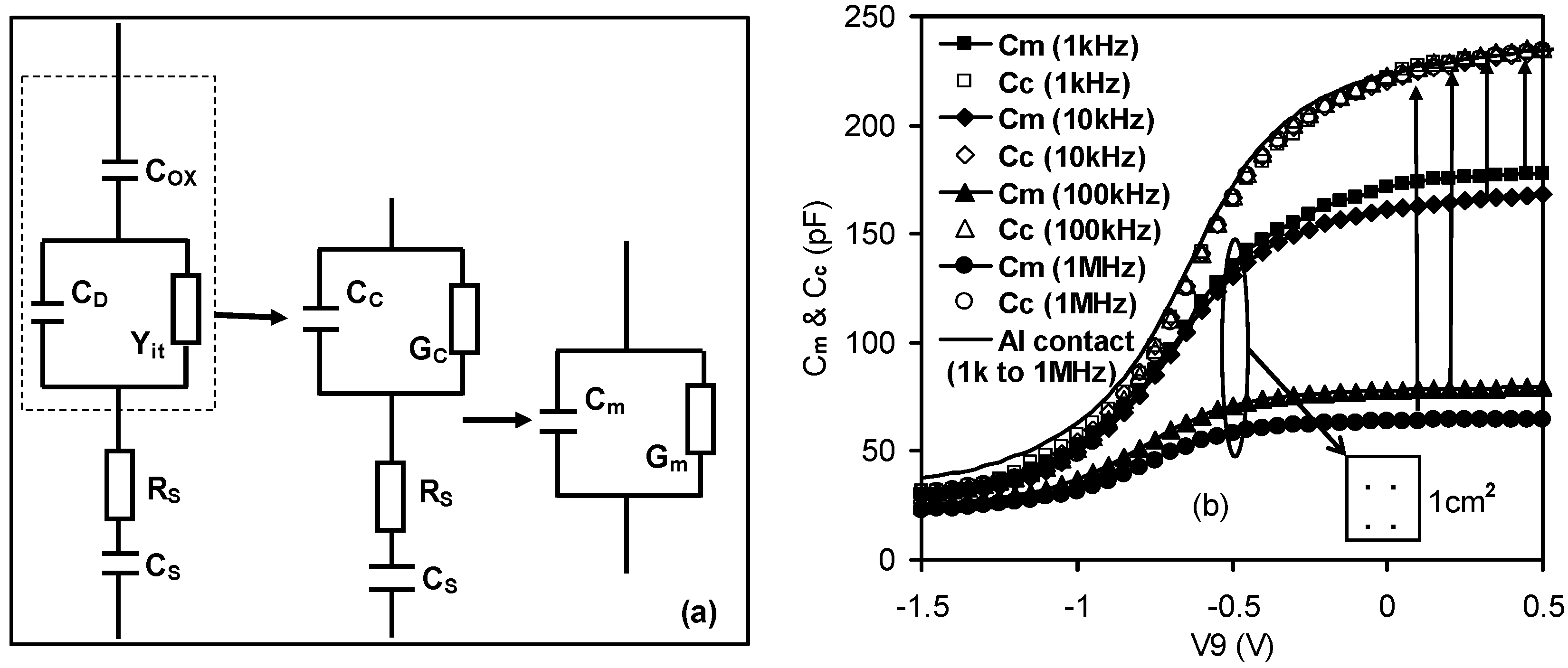
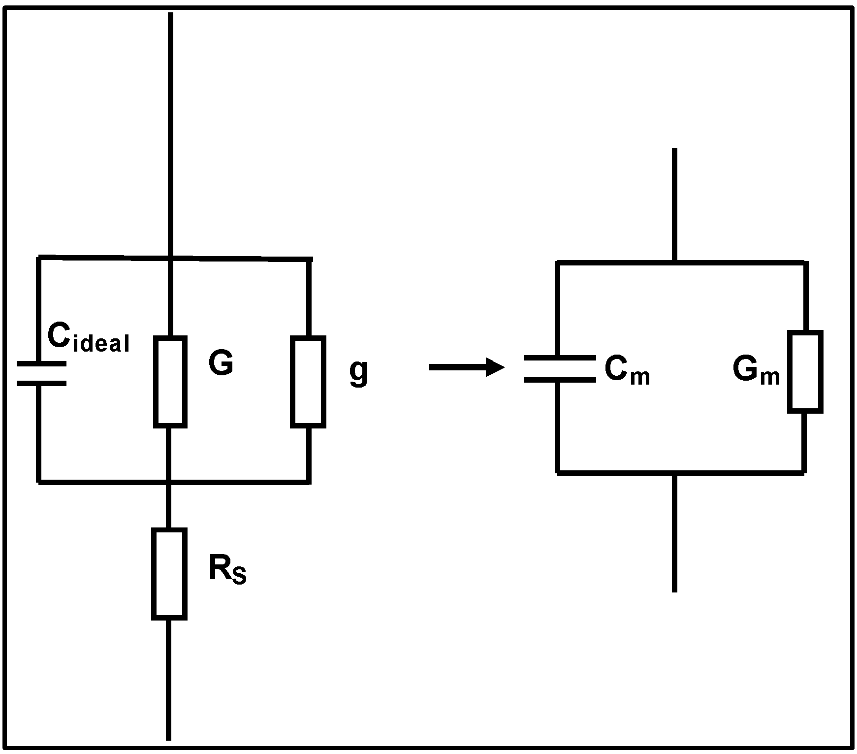
3.1.1. Parasitic Effect


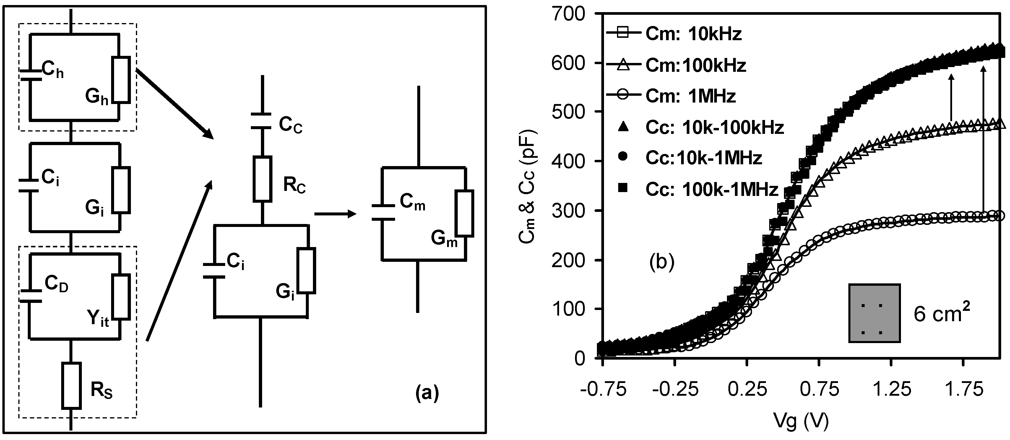
3.1.2. Lossy Interfacial Layer Effect


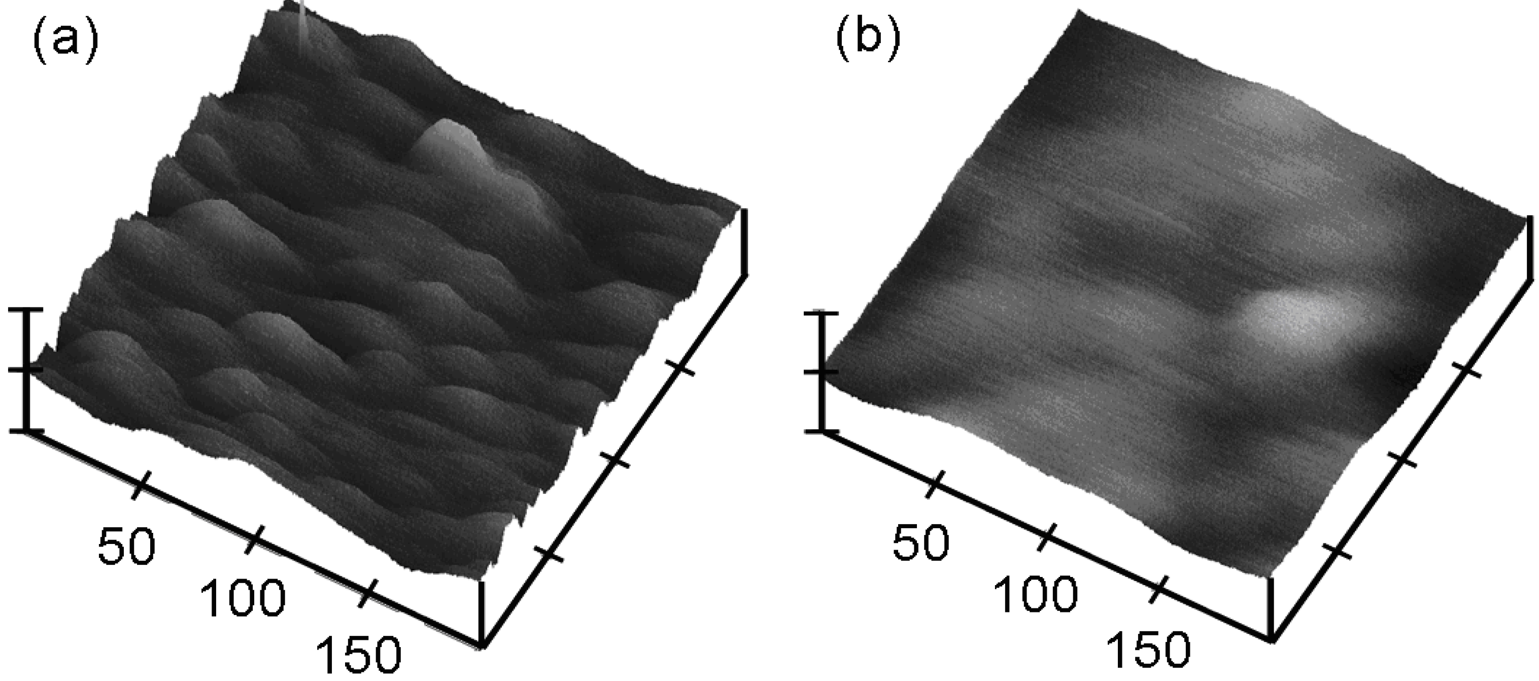
3.1.3. Surface Roughness Effect


3.1.4. Other Effects
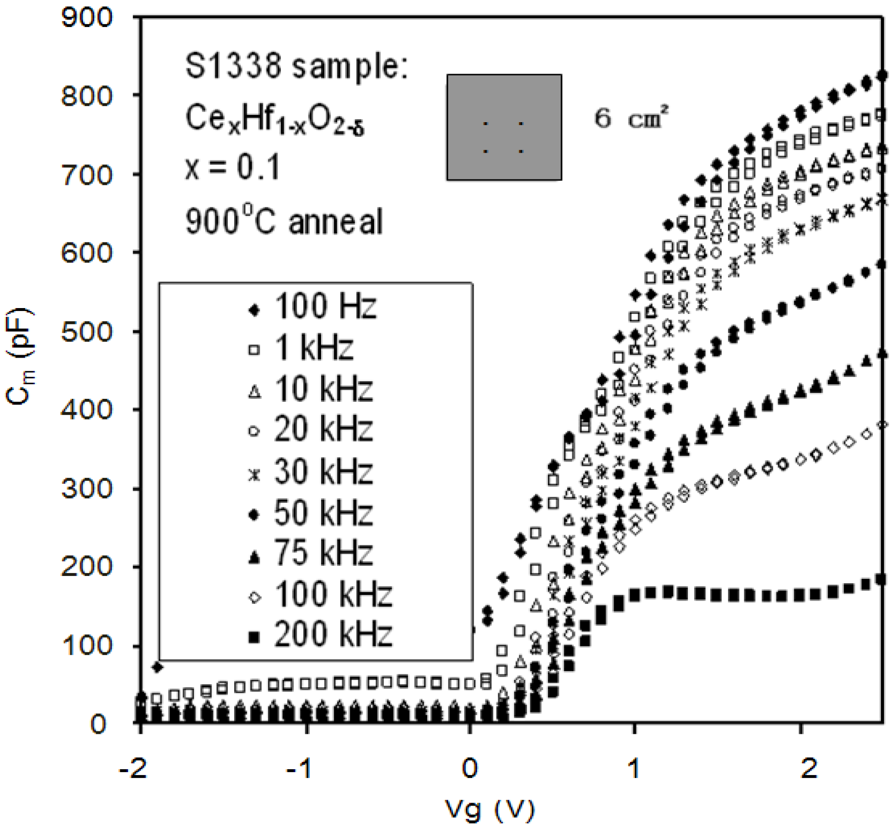
3.2. Intrinsic Causes of Frequency Dispersion During C-V Measurements
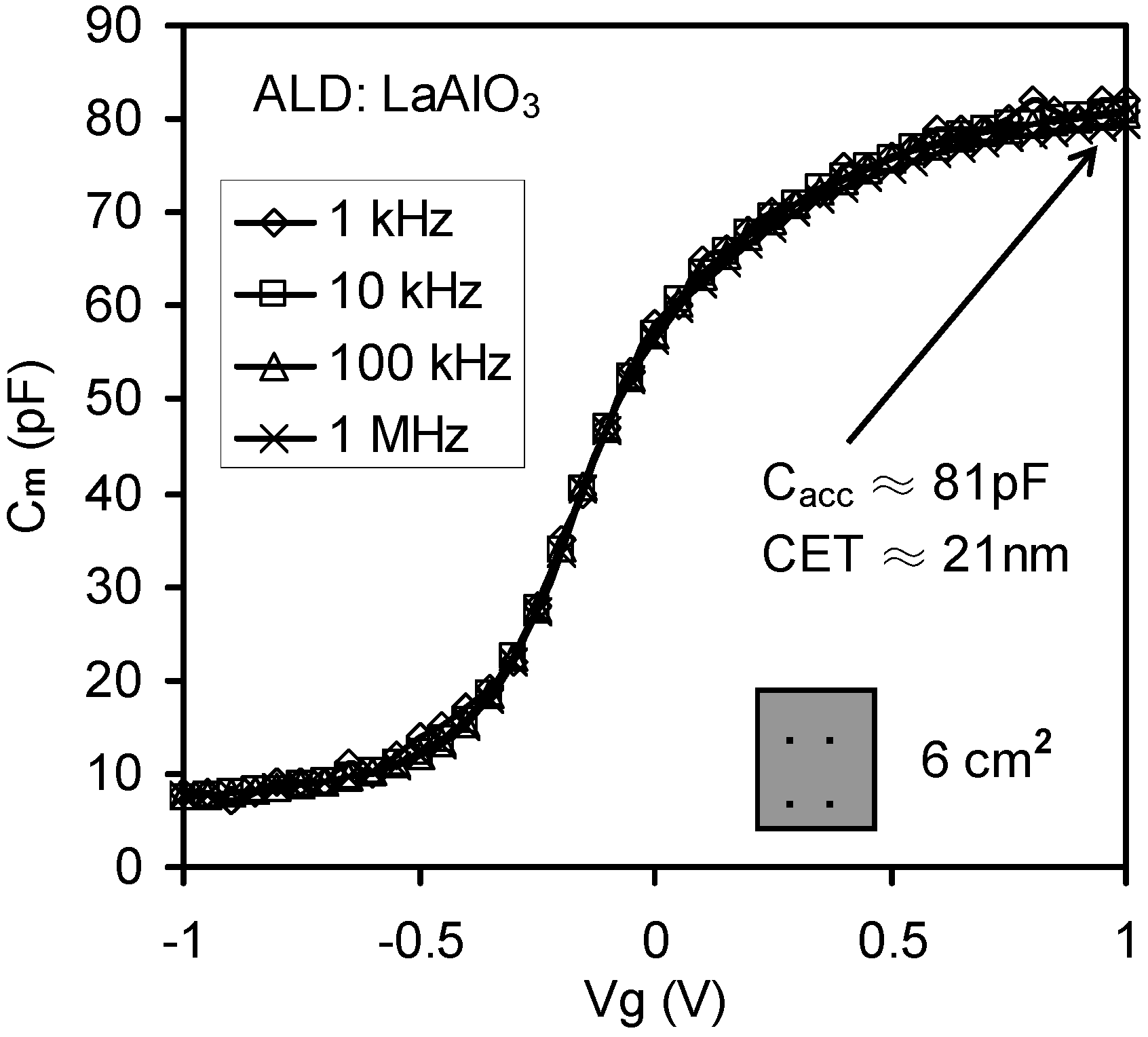
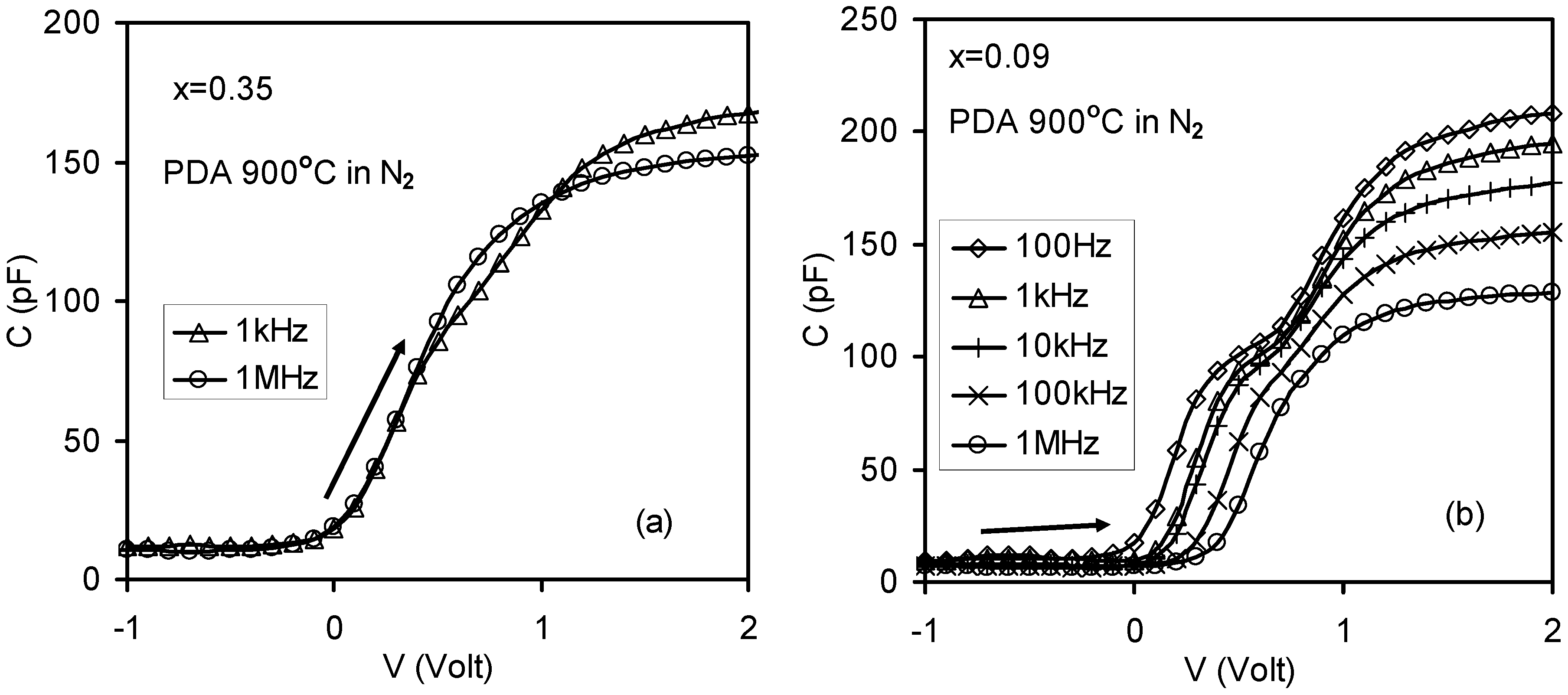
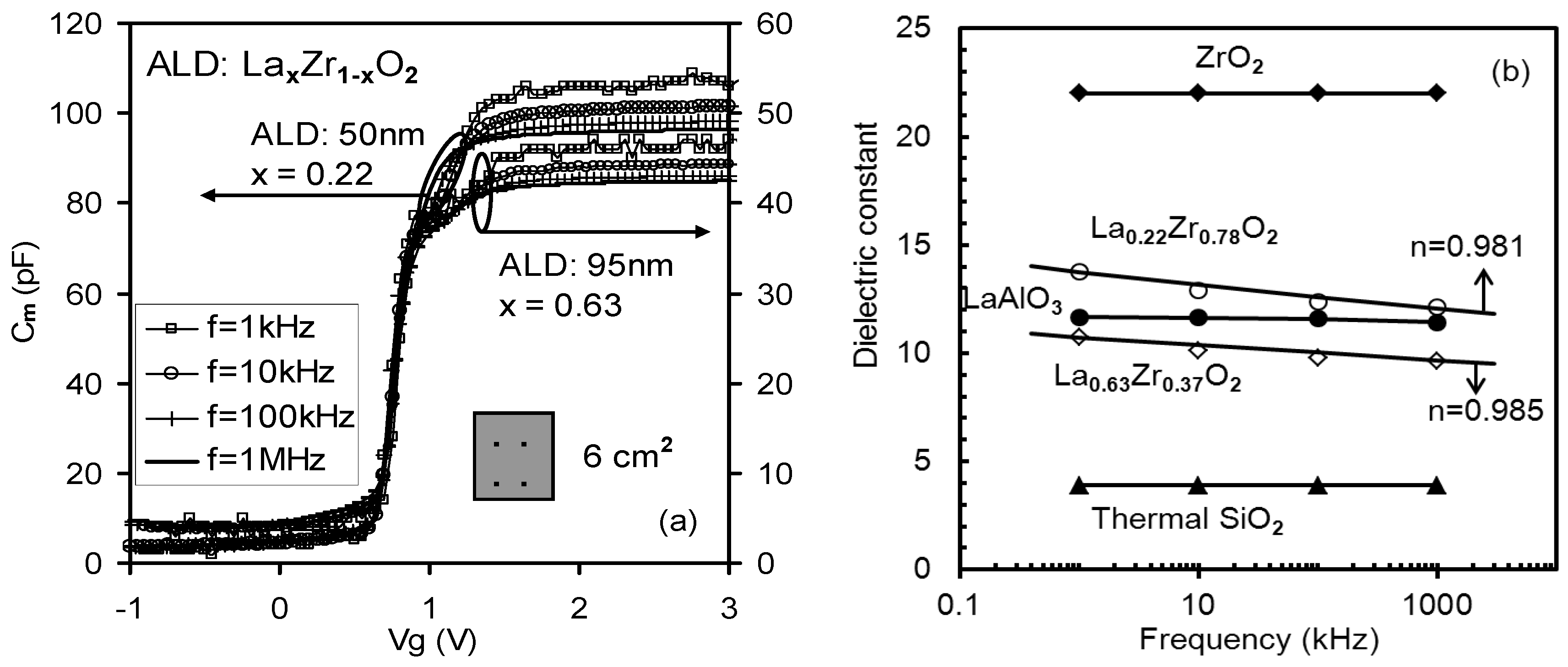
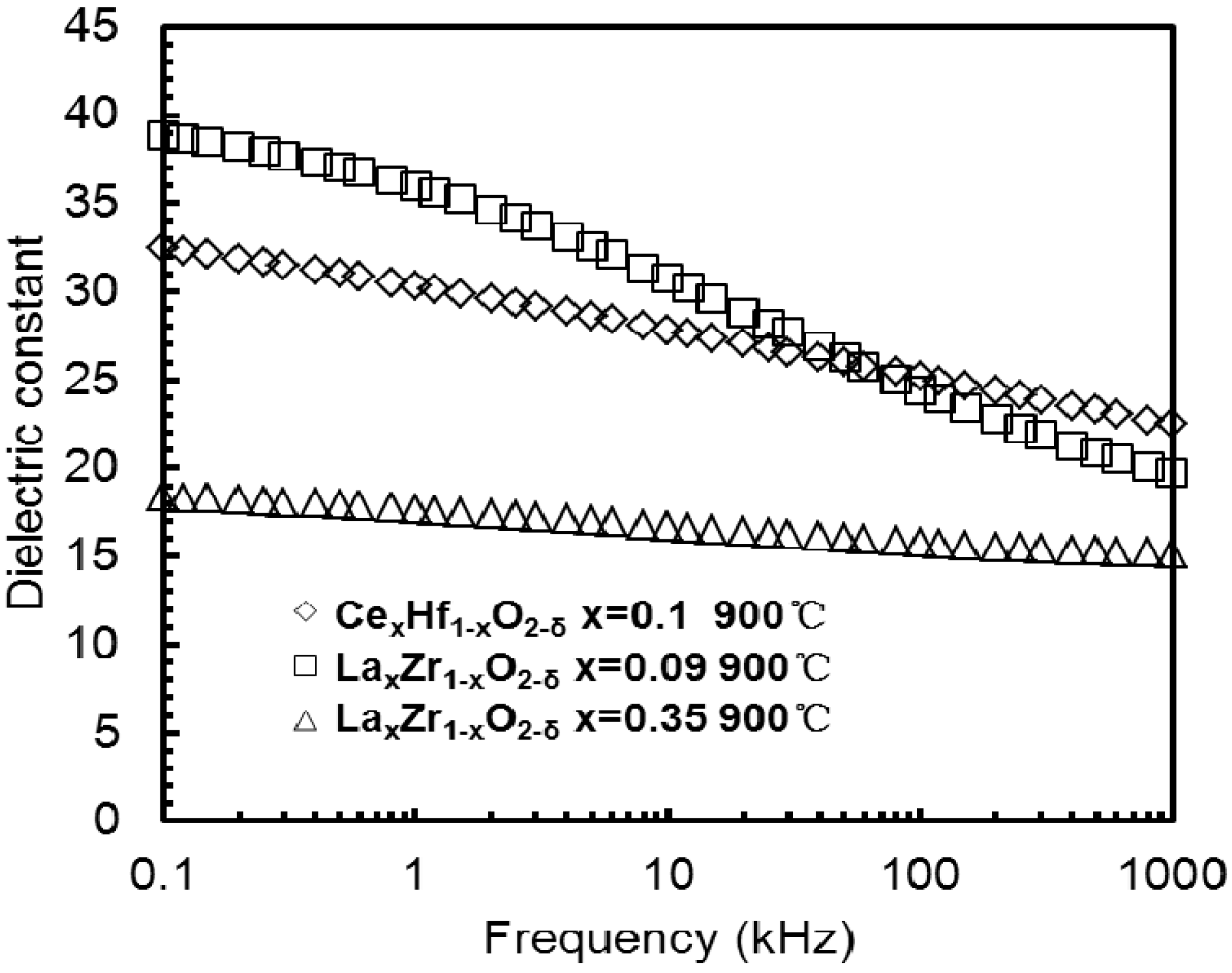
3.2.1. Frequency Dependence of k-Value


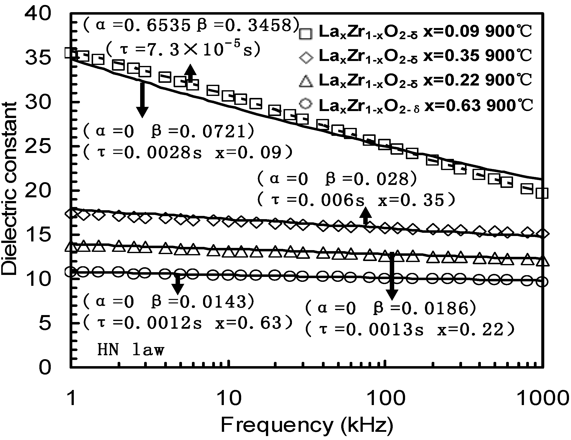
| Models | Cole-Cole | Cole-Davidson | Havriliak-Negami | ||||
|---|---|---|---|---|---|---|---|
| Parameters | α | τ (s) | β | τ (s) | α | β | τ (s) |
| LaxZr1–xO2–δ | 0.75 | 3.9 × 10⁻⁷ | 0.0721 | 0.0028 | 0.6535 | 0.3458 | 7.3 × 10⁻⁵ |
| x=0.09 | |||||||
| LaxZr1–xO2–δ | 0.866 | 4.6 × 10⁻¹¹ | 0.028 | 0.006 | 0 | 0.028 | 0.006 |
| x=0.35 | |||||||
| LaxZr1–xO2–δ | 0.815 | 3.8 × 10⁻¹¹ | 0.0186 | 0.0013 | 0 | 0.0186 | 0.0013 |
| x=0.22 | |||||||
| LaxZr1–xO2–δ | 0.82 | 5.2 × 10⁻¹² | 0.0143 | 0.0012 | 0 | 0.0143 | 0.0012 |
| x=0.63 | |||||||
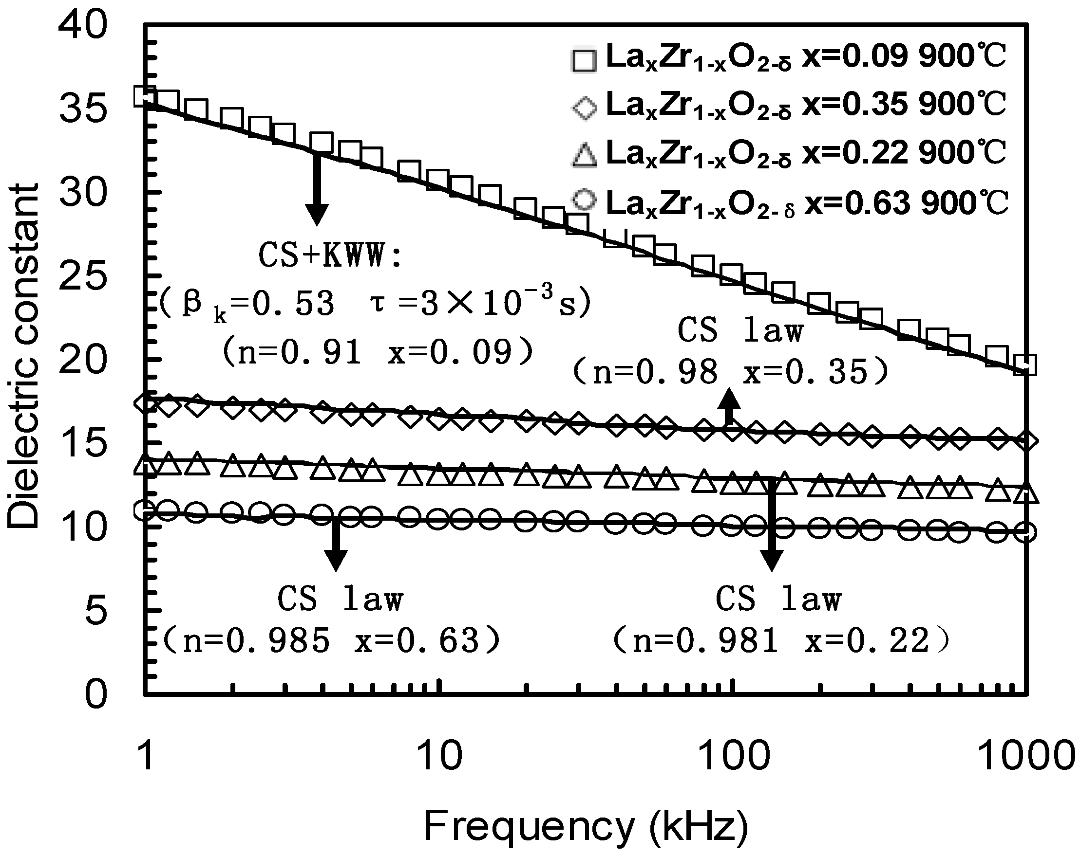
3.2.2. Dielectric Relaxation Models and Data Fitting

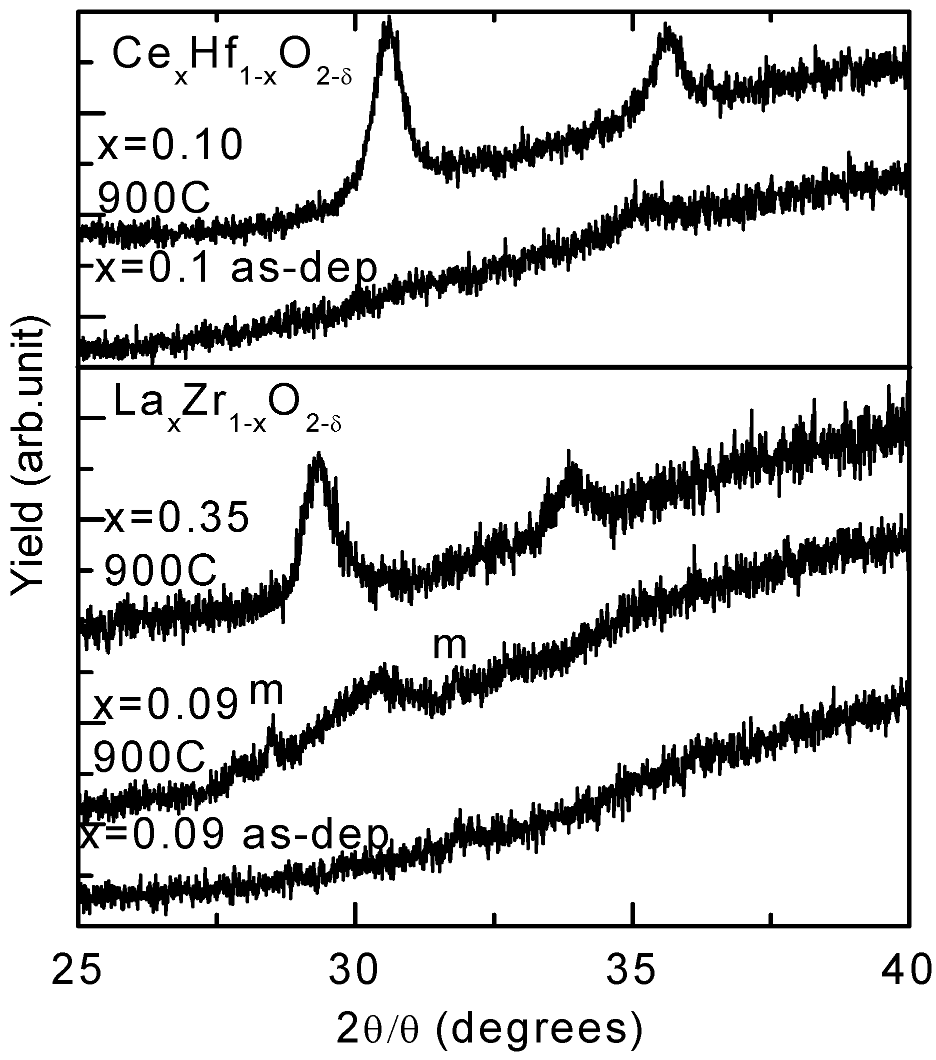
3.2.3. Dielectric Relaxation Mechanisms

4. Conclusions
Acknowledgement
References
- Juan, P.C.; Liu, C.H.; Lin, C.L.; Ju, S.C.; Chen, M.G.; Chang, I.Y.K.; Lu, J.H. Electrical characterization and dielectric property of MIS capacitors using a high-k CeZrO4 ternary oxide as the gate dielectric. Jpn. J. Appl. Phys. 2009, 48, 1–5. [Google Scholar]
- Dong, G.F.; Qiu, Y. Pentacene thin-film transistors with Ta2O5 as the gate dielectric. J. Korean Phys. Soc. 2009, 54, 493–497. [Google Scholar] [CrossRef]
- Zhu, X.H.; Zhu, J.M.; Li, A.D.; Liu, Z.G.; Ming, N.B. Challenges in atomic-scale characterization of high-k dielectrics and metal gate electrodes for advanced CMOS gate stacks. J. Mater. Sci. Technol. 2009, 25, 289–313. [Google Scholar] [CrossRef]
- International Technology Roadmap for Semiconductors Home page. Available online: http://public.itrs.net/ (accessed on 17 May 2012).
- Ricco, B.; Olivo, P.; Nguyen, T.N.; Kuan, T.S.; Ferriani, G. Oxide-thickness determination in thin-insulator MOS structures. IEEE Trans. Electron Devices 1988, 35, 432–438. [Google Scholar] [CrossRef]
- Terman, L.M. An investigation of surface states at a silicon/silicon oxide interface employing metal-oxide-silicon diodes. Solid State Electron. 1962, 5, 285–299. [Google Scholar] [CrossRef]
- Lee, S.W. A capacitance-based method for experimental determination of metallurgical channel length of submicron LDD MOSFET’s. IEEE Trans. Electron Devices 1964, 41, 403–412. [Google Scholar]
- Huang, C.L.; Faricelli, J.V.; Arora, N.D. A new technique for measuring MOSFET inversion layer mobility. IEEE Trans. Electron Devices 1993, 40, 1134–1139. [Google Scholar] [CrossRef]
- Sze, S.M. Physics of Semiconductor Devices; Wiley: New York, NY, USA, 1981. [Google Scholar]
- Yang, K.J.; Chenming, H. MOS capacitance measurements for high-leakage thin dielectrics. IEEE Trans. Electron Devices 1999, 46, 1500–1501. [Google Scholar] [CrossRef]
- Choi, C.H.; Wu, Y.; Goo, J.S.; Yu, Z.; Dutton, R.W. Capacitance reconstruction from measured C-V in high leakage nitride/oxide MOS. IEEE Trans. Electron Devices 2000, 47, 1843–1850. [Google Scholar] [CrossRef]
- Nicollian, E.H.; Brews, J.R. MOS (metal oxide semiconductor) physics and technology. In MOS (Metal Oxide Semiconductor) Physics and Technology; Wiley: NewYork, NY, USA, 2003. [Google Scholar]
- Kwa, K.S.K.; Chattopadhyay, S.; Jankovic, N.D.; Olsen, S.H.; Driscoll, L.S.; O’Neill, A.G. A model for capacitance reconstruction from measured lossy MOS capacitance-voltage characteristics. Semicond. Sci. Technol. 2003, 18, 82–87. [Google Scholar] [CrossRef]
- Hirose, M.; Hiroshima, M.; Yasaka, T.; Miyazaki, S. Characterization of silicon surface microroughness and tunneling transport through ultrathin gate oxide. J. Vac. Sci. Technol. A 1994, 12, 1864–1868. [Google Scholar] [CrossRef]
- Schuegraf, K.F.; King, C.C.; Hu, C. Impact of polysilicon depeletion in thin oxide MOS technology. In International Symposium on VLSI Technology, Systems and Applications-VLSI-TSA, Taipei, Taiwan, 12–14 May 2012; VLSI Technology: Seattle, WA, USA; pp. 86–90.
- Lee, S.W.; Liang, C.; Pan, C.S.; Lin, W.; Mark, J.B. A study on the physical mechanism in the recovery of gate capacitance to COX in implant polysilicon MOS structure. IEEE Electron Device Lett. 1992, 13, 2–4. [Google Scholar] [CrossRef]
- Spinelli, A.S.; Pacelli, A.; Lacaita, A.L. An improved formula for the determination of the polysilicon doping. IEEE Electron Device Lett. 2001, 22, 281–283. [Google Scholar] [CrossRef]
- Hauser, J.R.; Ahmed, K. Characterization of ultra-thin oxides using electrical C-V and I-V measurements. In AIP Conference Proceedings, Gaithersburg, MD, USA, November 1998; AIP: College Park, MD, USA; pp. 235–239.
- Pregaldiny, F.; Lallement, C.; Mathiot, D. Accounting for quantum mechanical effects from accumulation to inversion, in a fully analytical surface potential-based MOSFET model. Solid State Electron. 2004, 48, 781–787. [Google Scholar] [CrossRef]
- Sune, J.; Olivo, P.; Ricco, B. Quantum-mechanical modeling of accumulation layers in MOS structure. IEEE Trans. Electron Devices 1992, 39, 1732–1739. [Google Scholar] [CrossRef]
- Pregaldiny, F.; Lallement, C.; van Langevelde, R.; Mathiot, D. An advanced explicit surface potential model physically accounting for the quantization effects in deep-submicron. Solid State Electron. 2004, 48, 427–435. [Google Scholar] [CrossRef]
- Satter, M.M.; Haque, A. Modeling effects of interface trap states on the gate C-V characteristics of MOS devices on alternative high-mobility. Solid State Electron. 2010, 54, 621–627. [Google Scholar] [CrossRef]
- jiong, L.Z.; Ma, T.P. A new method to extract EOT of ultrathin gate dielectric with high leakage current. IEEE Electron Device Lett. 2004, 25, 655–657. [Google Scholar] [CrossRef]
- Bierwagen, O.; Geelhaar, L.; Gay, X.; Piešinš, M.; Riechert, H.; Jobst, B.; Rucki, A. Leakage currents at crystallites in ZrAlxOy thin films measured by conductive atomic-force microscopy. Appl. Phys. Lett. 2007, 90, 232901:1–232901:3. [Google Scholar]
- Böscke, T.S.; Govindarajan, S.; Kirsch, P.D.; Hung, P.Y.; Krug, C.; Lee, B.H. Stabilization of higher-tetragonal HfO2 by SiO2 admixture enabling thermally stable metal-insulator-metal capacitors. Appl. Phys. Lett. 2007, 91, 072902:1–072902:3. [Google Scholar] [CrossRef]
- Zhao, C.Z.; Taylor, S.; Werner, M.; Chalker, P.R.; Murray, R.T.; Gaskell, J.M.; Jones, A.C. Dielectric relaxation of lanthanum doped zirconium oxide. J. Appl. Phys. 2009, 105, 044102:1–044102:8. [Google Scholar]
- Gaskell, J.M.; Jones, A.C.; Aspinall, H.C.; Przybylak, S.; Chalker, P.R.; Black, K.; Davies, H.O.; Taechakumput, P.; Taylor, S.; Critchlow, G.W. Liquid injection ALD and MOCVD of lanthanum aluminate using a bimetallic alkoxide precursor. J. Mater. Chem. 2006, 26, 3854–3860. [Google Scholar] [CrossRef]
- Niwa, M.; Kouzaki, T.; Okada, K.; Udagawa, M.; Sinclair, R. Atomic-order planarization of ultrathin SiO2/Si (001) interfaces. Jpn. J. Appl. Phys. 1994, 33, 388–394. [Google Scholar] [CrossRef]
- Shiau, J.J.; Fahrenbruch, A.L.; Bube, R.H. Influence of ac contact impedance on high-frequency, low-temperature, or fast-transient junction measurements in semiconductors. J. Appl. Phys. 1987, 61, 1556–1561. [Google Scholar] [CrossRef]
- Venkatesan, V.; Das, K.; von-Windheim, J.A.; Geis, M.W. Effect of back contact impedance on frequency dependence of capacitance-voltage measurements on metal/diamond diodes. Appl. Phys. Lett. 1993, 63, 1065–1067. [Google Scholar] [CrossRef]
- Lo, S.H.; Buchanan, D.A.; Taur, Y.; Wang, W. Quantum-mechanical modeling of electron tunneling current from the inversion layer of ultra-thin-oxide nMOSFET’s. IEEE Electron Device Lett. 1997, 18, 209–211. [Google Scholar] [CrossRef]
- Taechakumput, P.; Zhao, C.Z.; Taylor, S.; Werner, M.; Pham, N.; Chalker, P.R.; Murray, R.T.; Gaskell, J.M.; Aspinall, H.C.; Jones, A.C. Origin of frequency of dispersion in high-k dielectrics. In Proceedings of 7th International Semiconductor Technology Conference ISTC2008, Shanghai, China, 15–17 March 2008; Electrochemical Society-Asia: Hong Kong, China; pp. 20–26.
- Zhao, X.; Vanderbilt, D. First-principles study of structural vibrational and lattice dielectric properties of hafnium oxide. Phys. Rev. B 2002, 65, 1–4. [Google Scholar]
- Wu, W.H.; Tsui, B.Y.; Huang, Y.P.; Hsieh, F.C.; Chen, M.C.; Hou, Y.T.; Jin, Y.; Tao, H.J.; Chen, S.C.; Liang, M.S. Two-frequency C-V correction using five-element circuit model for high-k gate dielectric and ultrathin oxide. IEEE Electron Device Lett. 2006, 27, 399–401. [Google Scholar] [CrossRef]
- Lerner, E.J. The end of the road for Moore’s law. IBM J. Res. Develop. 1999, 6, 6–11. [Google Scholar]
- Ahmed, K.; Ibok, E.; Yeap, G.C.F.; Qi, X.; Ogle, B.; Wortman, J.J.; Hauser, J.R. Impact of tunnel currents and channel resistance on the characterization of channel inversion layer charge and polysilicon-gate depletion of sub-20-A gate oxide MOSFET’s. IEEE Trans. Electron Devices 1999, 46, 1650–1655. [Google Scholar] [CrossRef]
- Choi, C.H.; Jung-Suk, G.; Tae-Young, O.; Yu, Z.P.; Dutton, R.W.; Bayoumi, A.; Min, C.; Voorde, P.V.; Vook, D.; Diaz, C.H. MOS C-V characterization of ultrathin gate oxide thickness (1.3–1.8 nm). IEEE Electron Device Lett. 1999, 20, 292–294. [Google Scholar] [CrossRef]
- Zhang, J.L.; Yuan, J.S.; Ma, Y.; Oates, A.S. Modeling of direct tunneling and surface roughness on C-V charateristics of ultra-thin gate MOS capacitors. Solid State Electron. 2001, 45, 373–377. [Google Scholar] [CrossRef]
- Arora, N.D.; Rios, R.; Huang, C.L. Modeling the polysilicon depletion effect and its impact on submicrometer CMOS circuit performance. IEEE Trans. Electron Devices 1995, 42, 935–943. [Google Scholar] [CrossRef]
- Rios, R.; Arora, N.D.; Huang, C.L. An analytic polysilicon depletion effect model for MOSFET's. IEEE Electron Device Lett. 1994, 15, 129–131. [Google Scholar] [CrossRef]
- Gupta, A.; Fang, P.; Song, M.; Lin, M.R.; Wollesen, D.; Chen, K.; Hu, C. Accurate determination of ultrathin gate oxide thickness and effective polysilicon doping of CMOS devices. IEEE Electron Device Lett. 1997, 18, 580–582. [Google Scholar] [CrossRef]
- Takeuchi, K.; Kasai, N.; Terada, K. A new effective channel length determination method for LDD MOSFETs. In IEEE 1991 International Conference on Microelectronic Test Structure, Kyoto, Japan, 18–20 March 1991; IEEE: New York, NY, USA; pp. 215–220.
- Cumberbatch, E.; Abebe, H.; Morris, H.; Tyree, V. Aanalytical surface potential model with polysilicon gate depletion effect for NMOS. In Proceedings of 2005 Nanotechnology conference, Anaheim, CA, USA, 8–12 May 2005; CRC Press: Boca Raton, FL, USA; pp. 57–60.
- Abebe, H.; Cumberbatch, E.; Morris, H.; Tyree, V. Numerical and analytical results for the polysilicon gate depletion effect on MOS gate capacitance. In Proceedings University/Government/Industry Microelectronics Symposium, San Jose, CA, USA, 25–28 June 2006; IEEE: New York, NY, USA; pp. 113–117.
- Lin, W.W. A simple method for extracting average doping concentration in the polysilicon and silicon surface layer near the oxide in polysilicon-gate MOS structures. IEEE Electron Device Lett. 1994, 15, 51–53. [Google Scholar] [CrossRef]
- Ohkura, Y. Quantum effects in Sin-MOS inversion layer at high substrate concentration. Solid State Electron. 1990, 33, 1581–1585. [Google Scholar] [CrossRef]
- Yeo, Y.C.; Ranade, P.; King, T.J.; Hu, C. Effects of high-k gate dielectric materials on metal and silicon gate work function. IEEE Electron Device Lett. 2002, 23, 342–344. [Google Scholar] [CrossRef]
- Sue, J.; Olivo, P.; Riccb, B. Quantum-mechanical modeling of accumulation layers in MOS structure. IEEE Electron Device Lett. 1992, 39, 1732–1739. [Google Scholar] [CrossRef]
- Moglestue, C. Self-consistent calculation of electron and hole inversion charges at silicon-silicon dioxide interfaces. J. Appl. Phys. 1986, 59(5), 3175–3183. [Google Scholar]
- Richter, C.A.; Hefner, A.R.; Vogel, E.M. A comparison of quantum-mechanical capacitance-voltage simulators. IEEE Electron Device Lett. 2001, 22, 35–37. [Google Scholar] [CrossRef]
- Debye, P. Polar Molecules; Chemical Catalogue Company: New York, NY, USA, 1929. [Google Scholar]
- Cole, K.S.; Cole, R.H. Dispersion and absorption in dielectrics. J. Chem. Phys. 1941, 9, 341–351. [Google Scholar] [CrossRef]
- Davidson, D.W.; Cole, R.H. Dielectric relaxation in glycerol, propylene glycol and n-propanol. J. Chem. Phys. 1951, 19, 1484–1490. [Google Scholar] [CrossRef]
- Raju, G.G. Dielectrics in Electric Fields; CRC Press: Boca Raton, FL, USA, 2003. [Google Scholar]
- Davidson, D.W.; Cole, R.H. Dielectric relaxation in glycerine. J. Chem. Phys. 1950, 18. [Google Scholar] [CrossRef]
- Bello, A.; Laredo, E. Distribution of relaxation times from dielectric spectroscopy using Monte Carlo simulated annealing: Application to α-PVDF. Phys. Rev. B 1999, 60, 12764–12774. [Google Scholar]
- Kliem, H.; Arlt, G. A relation between dielectric distribution functions and structural properties of amorphous matter. Annu. Rep. Conf. Electr. Insul. Dielectr. Phenom. 1987, 56, 325. [Google Scholar]
- Cabeza, M.; Keddam, M.; Novoa, X.R.; Sanchez, I.; Takenouti, H. Impedance spectroscopy to characterize the pore structure during the hardening process of Portland cement paste. Electrochim. Acta 2006, 51, 1831–1841. [Google Scholar] [CrossRef]
- Havriliak, S.; Negami, S. A complex plane analysis of α-dispersions in some polymer systems. J. Polym. Sci. Pt. C 1966, 14, 99–117. [Google Scholar] [CrossRef]
- Havriliak, S.; Negami, S. A complex plane representation of dielectric mechanical relaxation processes in some polymers. Polymer 1967, 8, 161–210. [Google Scholar] [CrossRef]
- Kalgaonkar, R.A.; Nandi, S.; Tambe, S.S.; Jog, J.P. Analysis of viscoelastic behavior and dynamic mechanical relaxation of copolyester based layered silicate nanocomposites using Havriliak-Negami model. J. Polym. Sci. B Polym. Phys. 2004, 42, 2657–2666. [Google Scholar] [CrossRef]
- Hartmann, B.; Lee, G.F.; Lee, J.D. Loss factor height and width limits for polymer relaxations. J. Acoust. Soc. Am. 1994, 95(1), 226–233. [Google Scholar]
- Jonscher, A.K. Dielectric Relaxation in Solids; Chelsea Dielectric Press: London, UK, 1983. [Google Scholar]
- Williams, G.; Watts, D.C. Non-symmetrical dielectric relaxation behaviour arising from a simple empirical decay function. Trans. Faraday Soc. 1969, 66, 80–85. [Google Scholar] [CrossRef]
- Bokov, A.A.; Ye, Z.G. Double freezing of dielectric response in relaxor Pb(Mg1/3Nb2/3)O3 crystals. Phys. Rev. B 2006, 74. [Google Scholar] [CrossRef]
- Ngai, K.L.; Plazek, D.J. A quantitative explanation of the difference in the temperature dependences of the viscoelastic softening and terminal dispersions of linear amorphous polymers. J. Polym. Sci. Polym. Phys. 1986, 24, 619–632. [Google Scholar] [CrossRef]
- Rendell, R.W.; Ngai, K.L.; Rajagopal, A.K. Volume recovery near the glass transition temperature in poly(vinyl acetate): predictions of a coupling model. Macromolecules 1987, 20, 1070–1083. [Google Scholar] [CrossRef]
- Ngai, K.L.; Fytas, G. Interpretation of differences in temperature and pressure dependences of density and concentration fluctuations in amorphous poly(phenylmethyl siloxane). J. Polym. Sci. Polym. Phys. 1986, 24, 1683–1694. [Google Scholar]
- Yoshihara, M.; Work, R.N. Dielectric relaxation in undiluted poly(4-chlorostyrene). II. Characteristics of the high-frequency tail. J. Chem. Phys. 1981, 74, 5872–5876. [Google Scholar] [CrossRef]
- Shioya, Y.; Mashimo, S. Comparison between interpretations of dielectric behavior of poly (vinyl acetate) by the coupling model and the Havriliak-Negami equation. J. Chem. Phys. 1987, 87, 3173–3177. [Google Scholar] [CrossRef]
- Boese, D.; Kremer, F.; Fetters, F.J. Molecular dynamics in bulk cis-polyisoprene as studied by dielectric spectroscopy. Macromolecules 1990, 23, 829–835. [Google Scholar] [CrossRef]
- Boese, D.; Momper, B.; Meier, G.; Kremer, F.; Hagenah, J.U.; Fischer, E.W. Molecular dynamics in poly(methylphenylsiloxane) as studied by dielectric relaxation spectroscopy and quasielastic light scattering. Macromolecules 1989, 22, 4416–4421. [Google Scholar] [CrossRef]
- Alvarez, F.; Alegria, A. Relationship between the time-domain Kohlrausch-Williams-Watts and frequency-domain Havriliak-Negami relaxation functions. Phys. Rev. B 1991, 44, 7306–7312. [Google Scholar] [CrossRef]
- Bokov, A.A.; Kumar, M.M.; Xu, Z.; Ye, Z.G. Non-arrhenius stretched exponential dielectric relaxation in antiferromagnetic TiBO3 single crystals. Phys. Rev. B 2001, 64. [Google Scholar] [CrossRef]
- Curie, J. Recherches sur le pouvoir inducteur specifique et sur la conductibilite des corps cristallises. Ann. Chim. Phys. 1889, 18, 385–434. [Google Scholar]
- Von Schweidler, E. Studien uber die anomalien im verhalten der dielektrika. Ann. Phys. 1907, 24, 711–770. [Google Scholar] [CrossRef]
- Lee, B.; Moon, T.; Kim, T.; Choi, D. Dielectric relaxation of atomic-layer-deposited HfO2 thin films from 1 kHz to 5 GHz. Appl. Phys. Lett. 2005, 87, 012901:1–012901:3. [Google Scholar]
- Costa, L.C.; Henry, F. Dielectric universal law of lead silicate glasses doped with neodymium oxide. J. Non-Cryst. Solids 2007, 353, 4380–4383. [Google Scholar] [CrossRef]
- Hoerman, B.H.; Ford, G.M.; Wessels, B.W. Dielectric properties of epitaxial BaTiO3 thin films. Appl. Phys. Lett. 1998, 73(16), 2248–2250. [Google Scholar]
- Horikawa, T.; Makita, T.; Kuriowa, T.; Mikami, N. Dielectric Relaxation of (Ba, Sr)TiO3 thin films. Jpn. J. Appl. Phys. 1995, 34. [Google Scholar] [CrossRef]
- Werner, M.; Zhao, C.Z.; Taylor, S.; Chalker, P.R.; Potter, R.J.; Gaskell, J. Permittivity enhancement and dielectric relaxation of doped hafnium and zirconium oxide. In IEEE 16th International Symposium on the Physical and Failure Analysis of Integrated Circuits, Suzhou, China, 6–10 July 2009; IEEE: New York, NY, USA; pp. 625–627.
- Fischer, D.; Kersch, A. The effect of dopants on the dielectric constant of HfO2 and ZrO2 from first principles. Appl. Phys. Lett. 2008, 92, 012908:1–012908:3. [Google Scholar] [CrossRef]
- Dervos, C.T.; Thirios, E.; Novacovich, J.; Vassiliou, P.; Skafidas, P. Permittivity properties of thermally treated TiO2. Mater. Lett. 2004, 58, 1502–1507. [Google Scholar] [CrossRef]
- Choosuwan, H.; Guo, R.; Bhalla, A.S.; Balachandran, U. Low-temperature dielectric behavior of Nb2O5-SiO2 solid solutions. J. Appl. Phys. 2003, 93, 2876–2879. [Google Scholar] [CrossRef]
- Yu, H.; Liu, H.; Hao, H.; Guo, L.; Jin, C.; Yu, Z.; Cao, M. Grain size dependence of relaxor in CaCu3Ti4O12 ceramics. Appl. Phys. Lett. 2007, 91, 222911:1–222911:3. [Google Scholar]
- Sivakumar, N.; Narayanasamy, A.; Chinnasamy, C.N.; Jeyadevan, B. Influence of thermal annealing on the dielectric properties and electrical relaxation behavior in nanostructured CoFe2O4. J. Phys. Condens. Matter 2007, 19. [Google Scholar] [CrossRef]
- Zhao, C.Z.; Werner, M.; Taylor, S.; Chalker, P.R.; Jones, A.C.; Zhao, C. Dielectric relaxation of La-doped Zirconia caused by annealing ambient. Nanoscale Res. Lett. 2011, 6, 1–6. [Google Scholar]
© 2012 by the authors; licensee MDPI, Basel, Switzerland. This article is an open access article distributed under the terms and conditions of the Creative Commons Attribution license (http://creativecommons.org/licenses/by/3.0/).
Share and Cite
Tao, J.; Zhao, C.Z.; Zhao, C.; Taechakumput, P.; Werner, M.; Taylor, S.; Chalker, P.R. Extrinsic and Intrinsic Frequency Dispersion of High-k Materials in Capacitance-Voltage Measurements. Materials 2012, 5, 1005-1032. https://doi.org/10.3390/ma5061005
Tao J, Zhao CZ, Zhao C, Taechakumput P, Werner M, Taylor S, Chalker PR. Extrinsic and Intrinsic Frequency Dispersion of High-k Materials in Capacitance-Voltage Measurements. Materials. 2012; 5(6):1005-1032. https://doi.org/10.3390/ma5061005
Chicago/Turabian StyleTao, J., C. Z. Zhao, C. Zhao, P. Taechakumput, M. Werner, S. Taylor, and P. R. Chalker. 2012. "Extrinsic and Intrinsic Frequency Dispersion of High-k Materials in Capacitance-Voltage Measurements" Materials 5, no. 6: 1005-1032. https://doi.org/10.3390/ma5061005