
Oxides for Rectenna Technology
by
Ivona Z. Mitrovic
1,*, 
Saeed Almalki
1,
Serdar B. Tekin
1,*,
Naser Sedghi
1,
Paul R. Chalker
2 and
Stephen Hall
1 1
Department of Electrical Engineering and Electronics, University of Liverpool, Liverpool L69 3GJ, UK
2
School of Engineering, University of Liverpool, Liverpool L69 3GH, UK
*
Authors to whom correspondence should be addressed.
Materials 2021, 14(18), 5218; https://doi.org/10.3390/ma14185218
Submission received: 24 July 2021
/
Revised: 29 August 2021
/
Accepted: 1 September 2021
/
Published: 10 September 2021
(This article belongs to the Special Issue Physics, Electrical and Structural Properties of Dielectric Layers)
Abstract
:The quest to harvest untapped renewable infrared energy sources has led to significant research effort in design, fabrication and optimization of a self-biased rectenna that can operate without external bias voltage. At the heart of its design is the engineering of a high-frequency rectifier that can convert terahertz and infrared alternating current (AC) signals to usable direct current (DC). The Metal Insulator Metal (MIM) diode has been considered as one of the ideal candidates for the rectenna system. Its unparalleled ability to have a high response time is due to the fast, femtosecond tunneling process that governs current transport. This paper presents an overview of single, double and triple insulator MIM diodes that have been fabricated so far, in particular focusing on reviewing key figures of merit, such as zero-bias responsivity (β0), zero-bias dynamic resistance (R0) and asymmetry. The two major oxide contenders for MInM diodes have been NiO and Al2O3, in combination with HfO2, Ta2O5, Nb2O5, ZnO and TiO2. The latter oxide has also been used in combination with Co3O4 and TiOx. The most advanced rectennas based on MI2M diodes have shown that optimal (β0 and R0) can be achieved by carefully tailoring fabrication processes to control oxide stoichiometry and thicknesses to sub-nanometer accuracy.
1. Introduction
Renewable energy sources are a key element in the drive towards zero-carbon economy targets worldwide in the decades to come. There has been unprecedented research activity towards sustainable energy materials and devices. Our earth receives ~1000 W/m2 at sea level during clear weather conditions. The major component of this solar energy of over 50% is in the infrared region (IR). The mid-IR wavelength range from 1.5 to 20 μm is the most important since it is re-emitted from the earth’s surface as IR radiation from 8 to 14 μm with maximum emissivity at 10.6 µm (28.3 THz). It is this energy that remains untapped by current solar cell-based harvesting sources. Conventional photovoltaic (PV) renewable technology has been used to harvest only the energy from the visible spectrum (400 to 750 nm) of the sun. Furthermore, unlike the energy of solar panels being limited by daylight and climate conditions, the energy of infrared heat can be harvested day and night. The concept of a rectifying antenna (rectenna) is not new [1,2], and its efficient design and operation in the IR region has been intriguing scientists for several decades. The use of an antenna and rectifying diode has only been successfully demonstrated for energy collection at microwave and radio frequencies [3]. An important point is that contrary to the photovoltaic technology where the conversion efficiency is limited by the semiconductor band gap, rectennas can, theoretically, achieve 100% conversion efficiency [4,5,6]. As such, the rectenna technology sits at the frontiers of high-frequency electronic devices and nanophotonics applications, to name just a few: optical transceivers in communication systems [7], IR and optical detection [8,9], and biosensors [10].
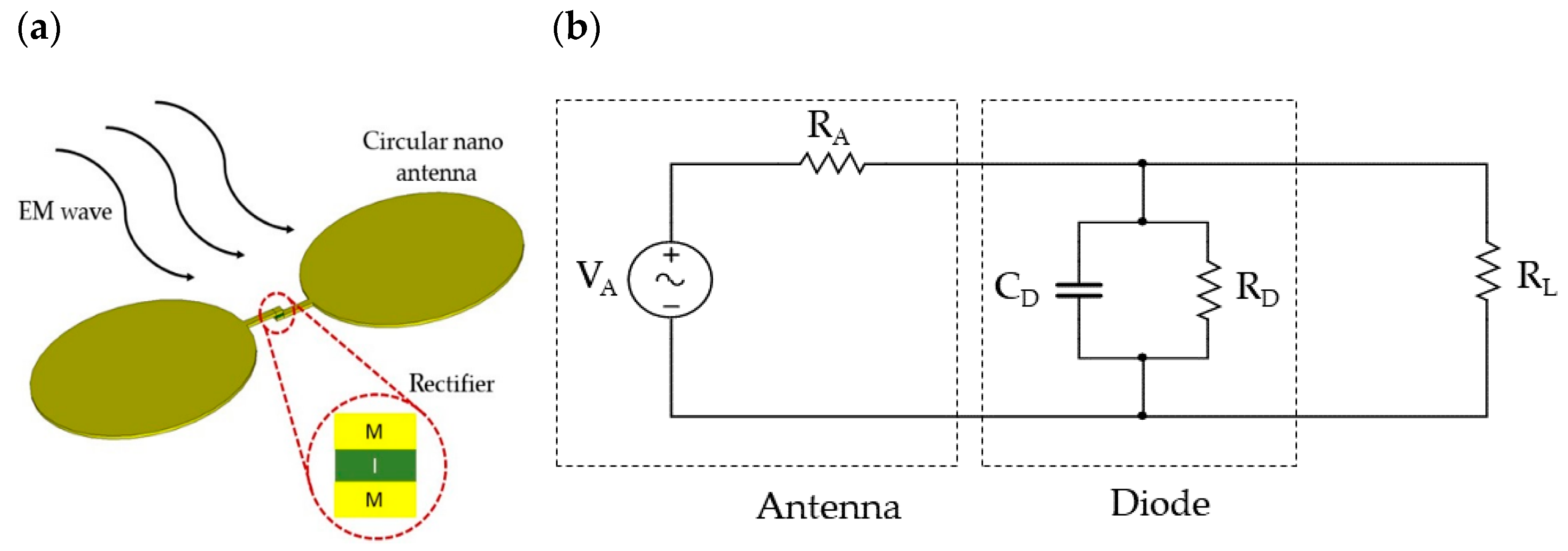
An optical rectenna consists of a receiving nano-antenna and a rectifying diode, as illustrated in Figure 1a. A metal-insulator-metal (MIM) diode has been considered as a prime contender for the rectenna system, and it is the main focus of review in this paper. The MIM diode can operate at terahertz (1 THz = 1012 Hz) frequencies due to the tunneling current mechanism having the electron transit time in femtoseconds (10−15 s). The rectification involves converting the oscillating charges (the alternating current (AC) electromagnetic signal), provided by the antenna arms flowing through the insulating thin film of a MIM rectifier, into a direct current (DC) signal. A simple equivalent circuit of a rectenna is shown in Figure 1b. It consists of an alternating voltage source (VA) with associated antenna resistance (RA) in series with the diode part comprising of the dynamic resistance (RD) and diode capacitance (CD) in parallel with the load resistance RL.
For efficient terahertz rectification, low diode capacitance and dynamic resistance are mandatory. The cut-off frequency (fc) can be calculated as:
Lowering the diode capacitance can be achieved by fabricating an MIM diode with minimal area or using a thick dielectric, since
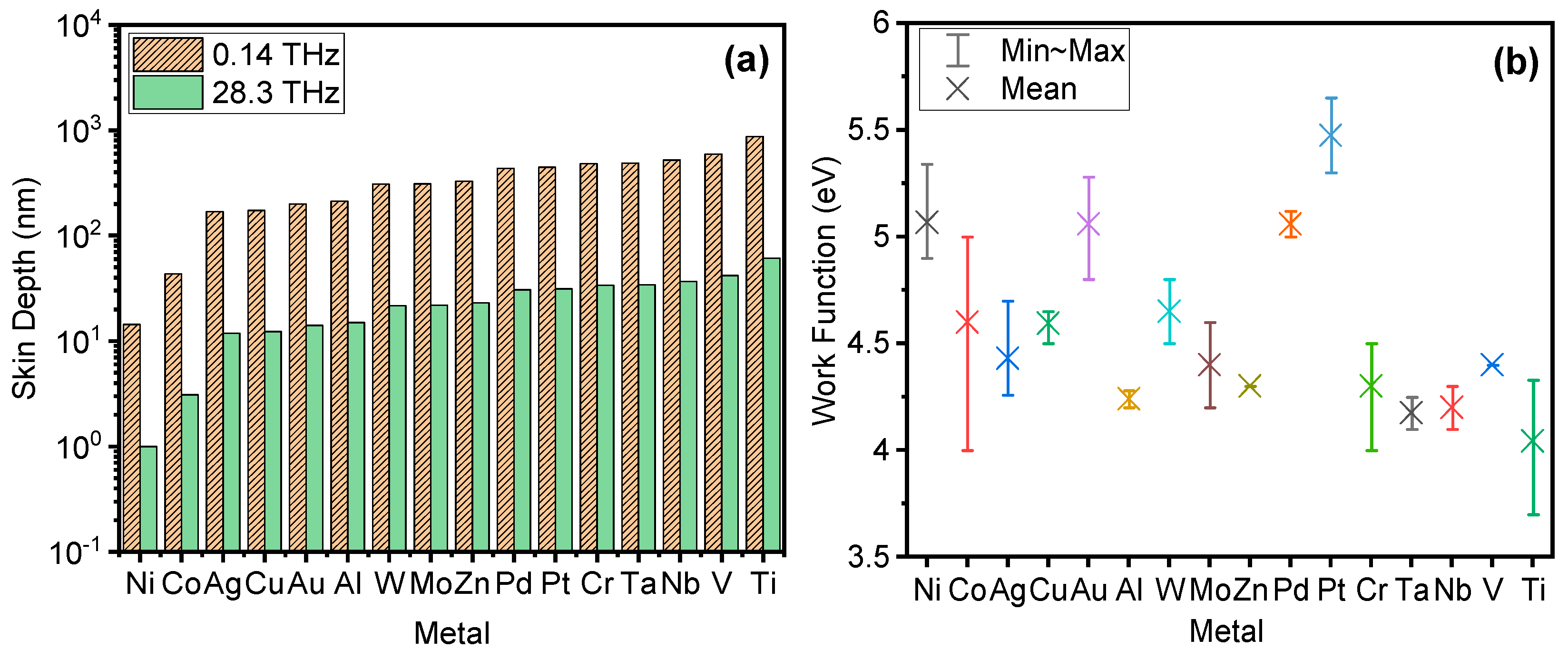
where is the thickness of the insulator, —its relative permittivity, —permittivity of vacuum and A is the diode area. However, increasing the oxide thickness will increase the diode resistance, which leads to a reduction of the electron tunneling probability through a wider energy barrier. Moreover, the insulator thickness should be in the range of a few nanometers so that electron tunneling dominates other parasitic transport mechanisms. The selection of materials for both metals and insulators as well as the insulator thickness control the diode electrical characteristics. A selection of typical metals that have been used in MIM diode fabrication is shown in Figure 2 and Table 1 with values of work function as reported in the literature [11,12,13,14,15,16,17,18,19,20]. At terahertz frequencies, the metal conductivity decreases, hence the skin effect should be considered. It can be calculated using Equation (3) for each metal, where the thickness of metal should be about five times the skin depth value to maintain good conductivity in the metal at a high-frequency regime:
where is the skin depth, is the resistivity of metal, is relative magnetic permeability of the metal, is the magnetic permeability of vacuum and f is the operating frequency. The skin depths for frequently used metals in rectennas that can operate at 0.14 and 28.3 THz are shown in Figure 2a and calculated using and in [21,22,23,24,25,26]. It can be seen that Ni has the smallest skin depth, and some of the first successful demonstrations of bowtie rectenna designs were realized using Ni-NiO-Ni diodes [27,28]. In terms of work function, the lowest values have Co, Cr and Ti, although there is a large range of values reported, especially for the former two metals (Table 1, Figure 2b) [11,13,15,16]. Furthermore, conductive oxides (indium tin oxide (ITO) and SrRuO3 (SRO)) and nitrides (TiN and NbN, see References in [29]) as well as multicomponent amorphous metals (ZCAN (ZrCuAlNi) and TiAl3) [18,30,31] can also act as electrodes in MIM diodes.
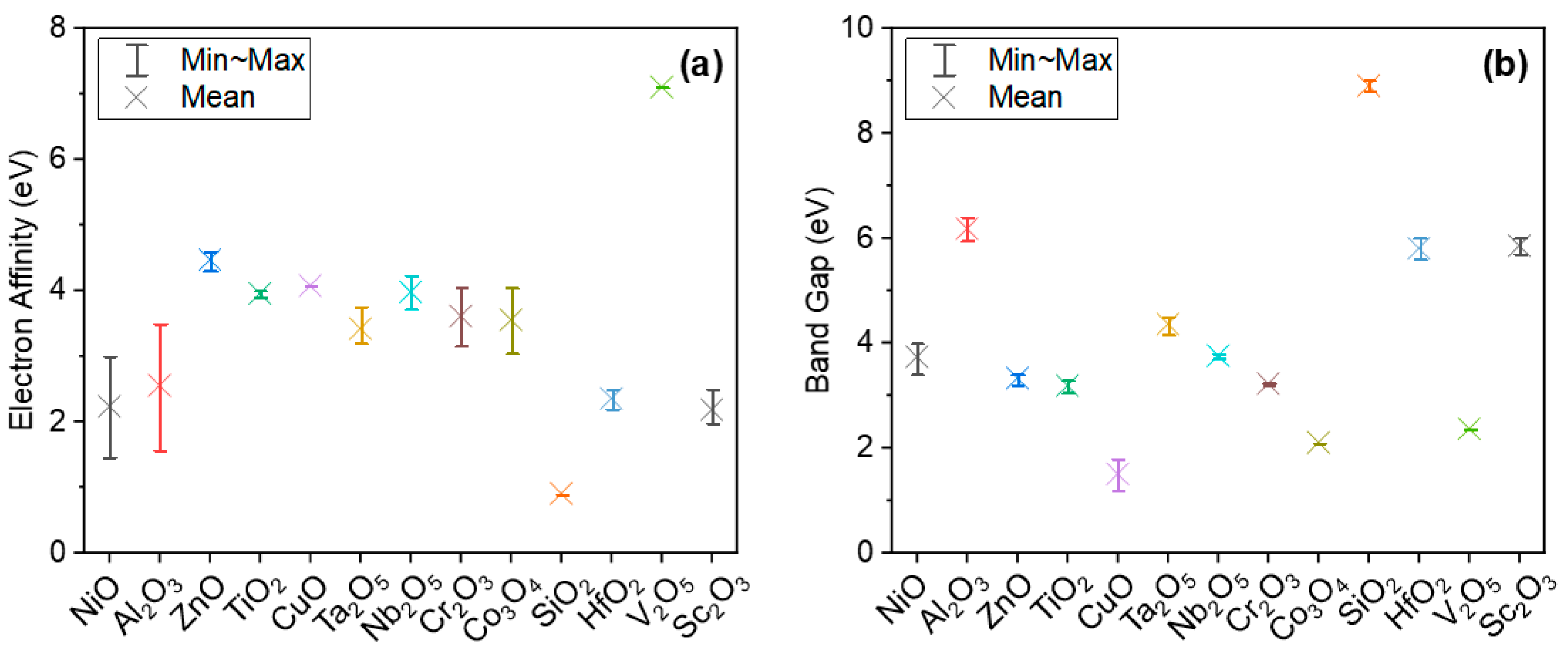
Figure 3a,b present electron affinities [9,17,32,33,34,35,36,37,38,39,40,41,42,43,44] and band gap [33,35,36,38,43,45,46,47,48,49,50,51,52,53,54,55] of typical oxides that have been used in the design and fabrication of MIM diodes. Full details are listed in Table 1 for completeness. Note that the large variation of reported values for electron affinity for Al2O3, NiO, Co3O4 and Cr2O3 is likely to be related to the variations in fabrication conditions. Changes in work function and χ can be up to 1 eV for metals and semiconductors depending on the surface conditions. These changes are likely to be due to the formation of electronic dipoles at the surface, changing the minimum energy for an electron to leave the sample [45]. Furthermore, the reported measured values of oxide band gap (Table 1) are found to vary depending on the stoichiometry and structural properties (amorphous, crystalline, polycrystalline) of films fabricated by different deposition techniques. As can be seen from Table 1, the band gap of amorphous Al2O3 thin films prepared by atomic layer deposition (ALD) [38] or molecular beam epitaxy [47] is found to be ~6.4 eV, while non-stoichiometric AlOx prepared by radio frequency (RF) sputtering exhibits a smaller band gap of 5.95 eV [45]. Another example is crystalline Sc2O3 films measured to have a band gap of 6.0 eV, while amorphous films have smaller values of ~5.7–5.8 eV [43]. Crystalline NiO was found to have a band gap of ~4.0 eV [46], while the most recent study shows a much smaller value of 3.4 eV for an RF-sputtered, 2 nm NiO film [45]. It is worth mentioning also that the variation of ±0.25 eV in reported band gap values in Table 1 could also be due to tolerances in using different characterization techniques to measure the band gap; that is, for Ta2O5, 4.2 eV from UV-vis (ultra violet-visible) absorbance spectra [35] in comparison to ~4.4 eV measured by reflection electron energy loss spectroscopy [38] or variable angle spectroscopic ellipsometry [51].
As stated in Equation (1), to achieve very small resistance × capacitance (RC) time constant and harvest IR energy, a trade-off between different physical parameters of diodes often limits practical implementation in rectennas. A number of significant issues need to be overcome, including (i) a precise manufacturing process with smooth metal electrodes and high-quality ultra-thin oxides, (ii) patterning of nano-scale devices as well as (iii) coupling efficiency and diode integration with the antenna. A rough metal surface affects oxide uniformity and hence the diode’s electrical characteristics. This eventually reduces the yield of functioning devices. Furthermore, even a small variation in oxide thickness largely affects the tunneling probability and the resulting current density of the diode due to the exponential relationship between current and electric field. Moreover, any defects present in the oxide film in the form of pinholes or traps may also give rise to undesirable conduction mechanisms such as Schottky and Poole Frenkel (PF) emission or trap assisted tunneling (TAT). Hence, growing or depositing a uniform, thin and defect-free insulator is a crucial step for efficient and reliable operation of a diode. Among several deposition methods, atomic layer deposition offers the best quality oxides with low defect density, excellent stoichiometry and superb uniformity [56]. The nano-scale patterning, to facilitate small diode area, requires the use of the most advanced ultra-fine mask-less lithographic techniques such as electron beam lithography. The latter can allow small capacitance while keeping resistance in the order of up to 100 Ω to match the antenna.
Another important point is that it is preferable to have a self-biased rectenna that operates without any external bias, so-called zero-bias rectenna. Furthermore, in practice, arrays of rectennas will be required to increase the collected power to useful levels. This can lead to a more efficient, higher, DC output power to the load.
Efficient IR frequency rectification requires nonlinear DC current−voltage (I-V) characteristics. The key MIM diode rectification figures of merit that can be determined from I-V characteristic are asymmetry, responsivity, nonlinearity and dynamic resistance. The asymmetry (ηasym) is defined as the absolute ratio of positive () to negative current (), or vice versa at a specific bias voltage:
Small signal rectification, however, is governed by nonlinearity around the operating point and is usually realized by square law rectification. A measure of small signal nonlinearity is responsivity, defined as the ratio of DC rectified current, IDC to input AC power, Pin [57], that is
where I′ and I″ are the first and second derivatives of current and gd is dynamic conductance at operating point Vp. Maraghechi et al. [58] have defined a nonlinearity factor as the ratio of dynamic to static conductance, that is
and also used the rate of change in nonlinearity to reflect the small signal nonlinearity. The dynamic resistance is defined as the inverse of the derivative of the current with respect to the applied voltage:
For MIM diodes, a particular interest is in dynamic resistance (R0 = 1/I′) and responsivity (β0 = I″/(2I′)) near zero-bias, as the self-biasing voltage is around millivolt. The latter is small due to generally poor coupling efficiencies that reduce the input power delivered to the MIM diode. Optimizing the parameters defined by Equations (4)–(7) from the DC I-V characteristics of the MIM diode can help in an improvement in the rectenna device performance under IR illumination.
This paper will present an overview of DC rectification parameters in the state-of-the-art single, double and triple MIM diodes with the aim of providing an outlook on their feasibility in IR nano-rectennas for real-life applications.
2. Overview of Metal Insulator Metal Diodes as Terahertz Rectifiers
2.1. Single Insulator MIM Diodes
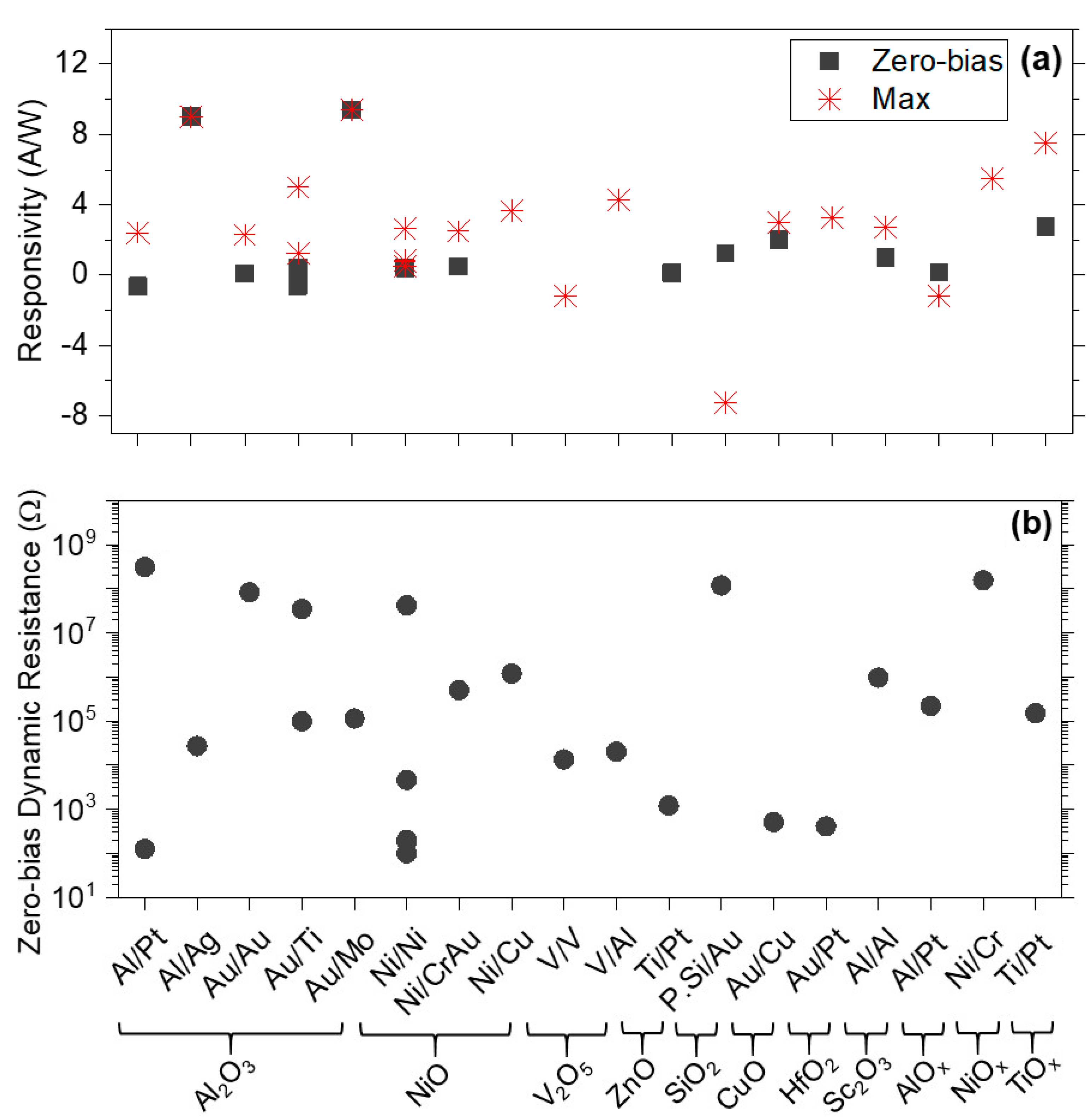
Various MIM diodes with different oxide layers and metal electrodes have been fabricated and characterized as depicted in Figure 4. A range of values for rectification figures of merit have been reported depending on the selection of materials, thickness of oxides, size of diodes and fabrication techniques, as listed in Table 2. It can be seen from Figure 4 and Table 2 that NiO [27,28,59,60,61,62,63,64,65,66,67,68,69] and Al2O3 [9,65,70,71,72,73,74,75] have been explored the most. The early work of Wilke et al. [27] and Fumeaux et al. [28] demonstrated the fabrication of ultra-small area diodes of 0.056 and 0.012 µm2, respectively, based on ~3.5 nm NiO combined with dipole, bowtie and spiral antennas. Although they demonstrated the operation of thin-film diode as mixers of 28 THz radiation for the first-time, there were issues with yield and repeatability of the fabrication process as well as low responsivity.
Hobbs et al. [76] demonstrated better responsivity and improved quantum efficiencies of 6% of waveguide-integrated near-infrared detectors based on antennas made of a multilayer Ni/Au stack that combines good IR properties of Au with the very low tunnel barrier (0.2 eV) of the Ni/NiO in MIM diodes. The geometric field enhancement technique in a Ni/NiO/Ni has been used by Choi et al. [61] to lower tunneling resistance and enhance the effective AC signal amplitude; The responsivity for this diode was superior to previously reported. Using Ni antennas makes it easy to grow NiO; However, Ni is very lossy in the infrared, especially at shorter wavelengths; Hence, there has been a resurgence of interest in fabricating NiO based diodes with other metals, such as Ag [64], Pt [65], CrAu [66,67], Cu [68] and Mo [69]. Krishnan et al. [66] realized a highly-sensitive diode (1.45 µm2 contact area) showing βMAX = 2.5 A/W at 0.1 V and zero-bias resistance of 500 kΩ using Ni/CrAu electrodes. By combining Ni/Cu electrochemical deposition and thermal oxidation for 2–12 nm NiO, Zhang et al. [68] reported diodes with a small area of 0.008 µm2, maximum responsivity of 3.65 A/W at 0.1 V but very high R0 of 1.2 MΩ. The responsivity could be further increased to 4.25 A/W by utilizing the same deposition technique for 6 nm NiO but using Ni/Ag [64]. Kaur et al. [69] reported reduced dynamic resistance to 6 kΩ when Ni/Mo electrodes were used and plasma oxidation for thin NiO film on a flexible substrate. Very high sensitivity (S = 2 × β) of 35 V−1 and resistivity of ~100 Ω at 0.6 V have been reported for Ni/NiO/Au diodes fabricated by the Langmuir–Blodgett method [63]; However, no zero-bias values are stated.
Alumina (Al2O3) is another oxide contender for MIM high-frequency applications [9,65,70,71,72,73,74,75]. Kinzel et al. [72] have demonstrated a slot-antenna-based frequency selective surface with integrated Al/Al2O3/Pt diodes showing zero-bias resistivity of 124.6 Ω. Bean et al. [71] have fabricated a dipole antenna-coupled Al/Al2O3/Pt detector using electron beam lithography and shadow evaporation metal deposition. Its specific detectivity for 28.3 THz radiation of 2.15 × 10⁶ cmHz1/2W−1 has been found to exceed IR detector performance based on Ni/NiO/Ni with 1 × 10⁶ cmHz1/2W−1 [59]. The highest zero-bias responsivity of ~9 A/W for Al2O3-based MIMs was achieved with Al/Ag [73] and Au/Mo [74] metal electrodes. Jayaswal et al. [9] designed a 28.3 THz rectenna using a bowtie nano-antenna coupled with the Au/Al2O3/Ti diode. Its zero-bias responsivity of 0.44 A/W and dynamic resistance of ~98 kΩ yielded an overall efficiency of the rectenna of 2.05 × 10⁻¹⁴.
There are a few studies of non-stoichiometric AlOx [29,77], TiOx [78,79] and NiOx [80] based MIMs, where the fabrication parameters are varied to control oxide thickness and hence optimize device responsivity and resistance. A very high asymmetry of 2500 and low zero-bias resistivity of 600 Ω have been achieved with Al/AlOx/Gr (graphene) electrodes [29]. The dipole antenna-coupled Al/AlOx/Pt has been demonstrated with associated IR detectivity of 9.65 × 10⁶ cmHz1/2W−1 [77].
Other oxides that have been considered for inclusion in MIM diodes include ZnO [81,82], V2O5 [20,83], SiO2 [84,85], Nb2O5 [86,87], CuO [8], TiO2 [69], Cr2O3 [88], HfO2 [89] and Sc2O3 [90]. A simple process for fabricating planar-type MIM tunneling diodes using electron beam writing and a boiling water oxidation process has been proposed, achieving high diode sensitivity of −31 V−1 for Poly Si/PolySi [85] and −14.5 V−1 for PolySi/Au electrodes [84] but too high R0. Very high asymmetry of 7700 at 0.5 V [87] and 9000 at 1 V [79] have been reported for Nb/Nb2O5/Pt and Gr/TiOx/Ti, respectively; however, no β0 and R0 were reported for these diodes. Gadalla et al. [8] demonstrated an Au/0.7 nm CuO/Cu diode with β0 = 2 A/W and R0 = 500 Ω. A similar low R0 of 405 Ω has been achieved by using Au/6 nm HfO2/Pt diode [89].
In summary, some diodes show high responsivity but also high dynamic resistance, which is undesirable for rectifying IR energy. An alternative way to enhance the figures of merit of MIM diodes is by using multiple insulators, which is now further discussed.
2.2. Multiple Insulator MInM Diodes, n = 2 and 3
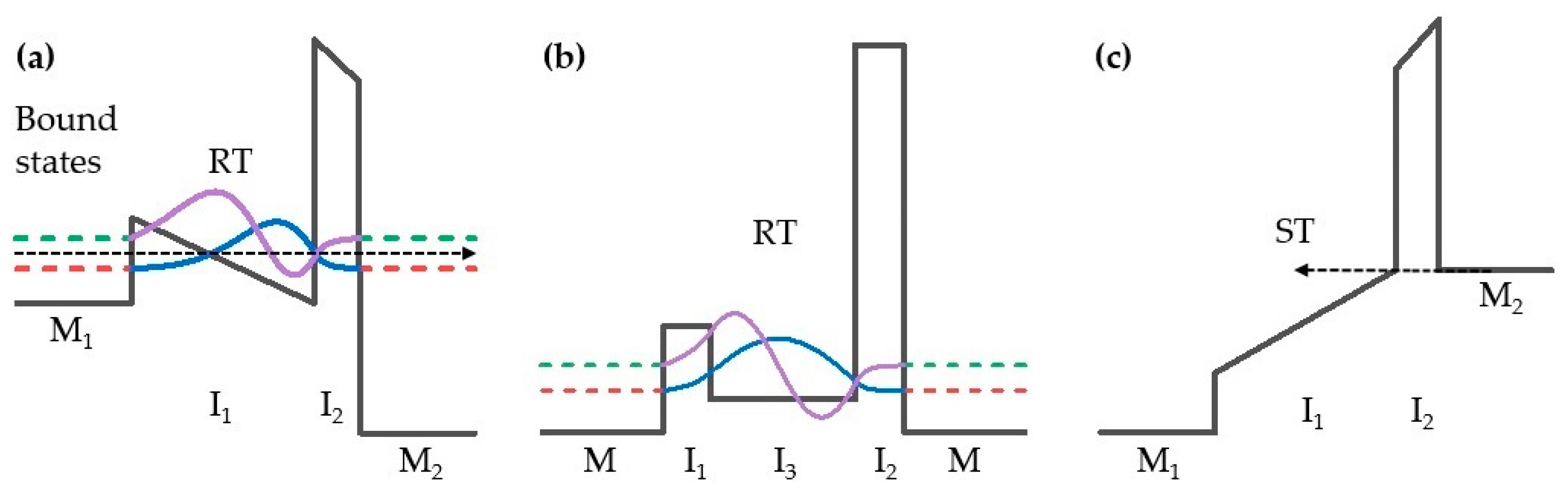
The performance of MIM diodes can be enhanced by using multiple insulator diodes (MInM) [91] that increase the nonlinearity of the I-V characteristics. There are two mechanisms that allow MInM diodes to have a high responsivity while keeping the resistance low [51,56,75,91]. First is to exploit the use of resonant tunneling (RT) of electrons through a quantum well formed between the two or three insulators (Figure 5a,b). In MI2M, this occurs when the metal Fermi level on the higher barrier side is positively biased, creating a right-triangular well at the interface of the two insulators (Figure 5a). Moreover, Figure 5b depicts a non-cascaded triple-insulator diode, where the deep quantum well already exists even at zero bias. There are localized eigenstates in this quantum well that are referred to as bound states and electrons can propagate through these energy states enhancing current transport [92,93].
On the other hand, step tunneling (ST) occurs for the opposite bias polarity in MI2M shown in Figure 5c, where an abrupt increase in current occurs when the metal Fermi level on the higher barrier side rises above the conduction band of the lower barrier, thereby decreasing the tunnel distance. In a particular device, the choice of insulator materials, metals and thicknesses determines the mechanism that dominates [18,51,56,58,94,95].
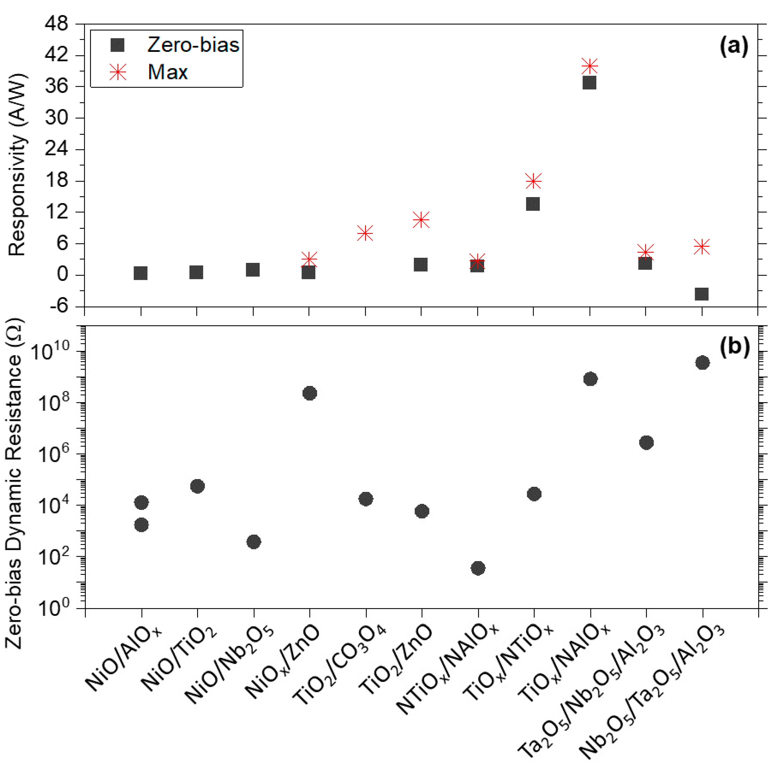
Figure 6 shows responsivity and zero-bias dynamic resistance values for MInM diodes (n = 2, 3) where both parameters have been reported.
Full details of rectification parameters, area and deposition technique for MInM diodes are listed in Table 3 for completeness. It can be seen that one of the MIM oxide contenders, Al2O3, has been explored in combination with lower band gap oxides, such as HfO2 [18,58], Ta2O5 [30,51,96], Nb2O5 [17,51], and most recently NiO [45,97]. Furthermore, NiO has been used in combination with TiO2 [14], Nb2O5 [98] and ZnO [80]. Recent work also explores MI2M diodes with TiO2 in combination with ZnO [99], TiOx [100] and Co3O4 [15], as well as nitrogen-doped TiO2 and Al2O3 films in a Pt/NTiOx/NAlOx/Al device [101].
The enhanced rectifying performance of a double insulator in comparison to single insulator diodes has been reported for Cr/Al2O3/HfO2/Cr diode by Maraghechi et al. [58]. Although promising in terms of enhanced asymmetry (>10 at 3 V), the nonlinearity at low bias was not engineered. Alimardani et al. [18,30] took a step forward in demonstrating experimentally the step tunneling mechanism in MI2M diodes based on Al2O3/HfO2 and Al2O3/Ta2O5 with a large work function difference (~0.6 eV) of metal electrodes, Al and ZCAN. Improved asymmetry and nonlinearity values were obtained at lower bias voltages (10 at 0.45 V); however, no zero-bias rectification parameters were reported. High asymmetry values of 18 at 0.35 V [51] and maximum responsivity of 6 A/W have been reported for Al/Al2O3/Ta2O5/Al, where a sharp increase in current at ~2 V has been ascribed to resonant tunneling. The latter was also observed in a Ni/NiOx/ZnO/Cr diode [80], showing high asymmetry of 16 at 0.5 V and βMAX = 8 A/W.
Mitrovic et al. [17] have further demonstrated a superior low-bias asymmetry of 35 at 0.1 V and a responsivity of 5 A/W at 0.25 V for the Nb/4 nm Nb2O5/1nm Al2O3/Ag diode. Moreover, the onset of strong resonance in the sub-V regime (<1 V) was found to be controlled by a work function difference of Nb/Ag electrodes in agreement with the experimental band alignment and theoretical model [17]. The model for calculating the bound states in a quantum well has been established [92,93], based on a modified multibarrier Tsu–Esaki method, whereby the insulator stack is assumed to consist of multiple slices with different barrier heights. The transmission amplitude at each energy level is found by solving the time-independent Schrodinger equation using the transmission matrix method. Using this model, Noureddine et al. [96] have also studied the effect of resonant tunneling on asymmetric Al/Ta2O5/Al2O3/Cr diodes with varied oxide thickness ratios 1:1, 1:2, 1:3 and 1:4 (in nm). They observed a good correlation between the thickness ratio of the insulating layers and the simulated bound states between the Ta2O5/Al2O3 conduction bands. The rectifying characteristics of the diodes have been improved at low turn-on voltages down to 0.17 V [102]. It is worth mentioning that none of the devices reported above were of adequately small area, which is required for integration with the antenna part; rather different metal/oxide configurations were used to engineer a diode with improved asymmetry and nonlinearity.
Herner et al. [15] investigated the relationship between responsivity and resistance in MI2M diodes. They fabricated Co/Co3O4/TiO2/Ti diodes of various thicknesses and under different annealing temperatures. A significant reduction in the dynamic resistance with a slight decrease in the responsivity has been observed after annealing of the samples up to 256 °C in air. The best performing diodes have β0 = 2.2 A/W and R0 = 18 kΩ (Table 3). In a later study [14], the zero-bias rectification performance of a Co3O4-based diode was compared to a Ni/NiO/TiO2/Cr structure. A theoretical quantum mechanical MIM diode simulator was used to analyze the responsivity-resistance correlation for both diodes by varying the insulator thickness. Step tunneling has been observed as the dominant conduction mechanism in both structures rather than resonant tunneling. It has been concluded that resonant tunneling is a crucial factor in reducing the dynamic resistance. The latter could be achieved by increasing the Co3O4 thickness but comes with a requirement of a higher bias voltage. Another alternative suggested in [14] is the use of a so-called geometric diode [4], but this work is outside the scope of this paper.
Pelz et al. [98] fabricated a travelling-wave diode (TWD) composed of Ni/NiO/Nb2O5/CrAu to demonstrate that the transmission line impedance can overcome the RC time constant limitations of the conventional MIM diodes at optical frequencies. According to DC I-V measurements, dynamic resistance of 380 Ω and responsivity of 0.46 A/W were achieved at zero-bias (Table 3). In the optical measurements, the TWD exhibited peak responsivity of 130 µA/W and the detectivity of 1.0 × 10⁴ jones. Elsharabasy et al. [99] demonstrated a Ti/TiO2/ZnO/Al diode with a peak responsivity of 10.6 A/W at 0.15 V, R0 = 5.9 kΩ and β0 = 1.9 A/W. Their optimized rectenna design parameters have been determined by a genetic algorithm and found to have theoretically 5.5% coupling efficiency, 6.4 A/W responsivity and 34 THz cut-off frequency.
A recent important report by Matsuura et al. [100] demonstrates Pt/TiO2/TiO1.4/Ti asymmetric diodes composed of stoichiometric and non-stoichiometric oxide layers with the aim of increasing current density and hence asymmetry. The latter increase has been found for non-stoichiometric TiOx, where the diode exhibited a current density of 4.6 × 10⁶ A/m2 and a peak asymmetry of 7.26 at 0.45 V. By exploring a similar concept as in [100], Weerakkody et al. [45] found that Ni/NiO/AlOx/CrAu diodes could achieve low R0 = 1.75 kΩ and reasonable high β0 = 0.31 A/W. This was achieved by engineering the electron affinity of Al2O3 by modifying its deposition conditions so that it comprises mostly of Al3+ ions and hence has a higher electron affinity value of 3.26 eV (the value for thin stoichiometric Al2O3 is ~1.6 eV [17]) and hence a much lower barrier with NiO. The bowtie antenna realized with this diode, designed to operate at 28.3 THz, has shown significant improvement in overall conversion efficiency of 3.7 × 10⁻⁸% and detectivity of 1.7 × 10⁵ cmHz1/2W−1. Another recent breakthrough is that resonant quasi-bound states can be reached at near 0 V, where Ni/NiO/AlOx/CrAu diodes self-bias when illuminated at 30 THz by the antenna part. By modifying the depth and width of the quantum well (Figure 5a) of a 0.035 μm2 diode by changing insulator thicknesses, low R0 = 13 kΩ and high β0 = 0.5 A/W were achieved simultaneously [97]. The resulting bowtie rectenna for diodes where RT has occurred shows improved power conversion efficiency of 1.7 × 10⁻⁸% [97]. The calculated coupling efficiency for this rectenna is found to be 5.1%, the highest achieved to date.
Another recent approach is defect engineering in MI2M diodes [101]. Nitrogen doping of TiO2 and Al2O3 using plasma-assisted ALD (PA-ALD) causes the generation of electron traps, which can assist unidirectional, defect-mediated PF transport and TAT in a multi-insulator stack. Although the latter have been found to increase rectifying performance of the doped diodes, it should be noted that the electron transport is considerably slower than tunneling, which could limit the frequency response. The best performing Pt/NTiOx/NAlOx/Al diode exhibits R0 = 36 Ω and β0 = 1.7 A/W.
The most recent theoretical study by Elsharabasy et al. [103] shows the optimization of the responsivity of MI2M diodes by considering metal/oxide properties and fixing the diode resistance to 100 Ω to match the nano-antenna impedance. The optimization has been performed to ensure zero-bias operation, and the diode configuration that fits the closest to the optimal solution has been found to be Ti/1 nm TiO2/1 nm Nb2O5/Ti, showing R0 = 108.6 Ω and β0 = 4.99 A/W from simulations. The RC time constant was found to be 9 fs for the diode area of 0.01 μm2, resulting in a 17 THz cut-off frequency.
In contrast to MI2M, there are comparatively fewer studies reported on triple-insulator diodes [56,75,104]. Maraghechi et al. [104] investigated and reported the resonant tunneling phenomenon for the first time in Cr/Cr2O3/HfO2/Al2O/Cr and Cr/Cr2O3/Al2O3/HfO2/Cr diodes in cascaded and non-cascaded configurations, respectively. Further work of Mitrovic et al. [56,75] demonstrated cascaded (Al/Nb2O5/Al2O3/Ta2O5/Al) and non-cascaded (Al/Ta2O5/Nb2O5/Al2O3/Al) diode configurations based on ultra-thin oxide films (1–3 nm) of Nb2O5, Al2O3 and Ta2O5 deposited by ALD. The diodes show strong tunneling and RT behavior at low voltages (0.35 V for non-cascaded configuration), substantiating evidence of the high-quality and uniqueness of atomic layer deposition that has been used to facilitate sub-nm thickness control, low oxide defect density, excellent stoichiometry and superb uniformity. The diodes exhibited a superior low-voltage responsivity of 5 A/W at 0.2 V and asymmetry of 12 at 0.1 V as the best performing MI3M diodes to date. The scaling of the contact area for these diodes is underway.
3. Permittivity and Scaling Issues
The quality of an oxide film determines the type and magnitude of the diode current. The majority of the fabricated MIM diodes shown in Table 2 have oxide thicknesses below 5 nm, which serves to facilitate quantum-mechanical tunneling. An uneven, non-uniform insulating layer can result in current crowding and hence variability and lack of reproducibility for MIM diodes. Other conduction mechanisms, such as PF emission or TAT, may arise due to oxide defects. Hence, the formation of a uniform, ultrathin (<10 nm) and defect-free insulator layer is essential. Several oxide deposition techniques are apparent, as listed in Table 2 and Table 3: native [65], plasma [15,60,61,62,66,67,69,73,78], thermal [29,64,68], boiling water [84,85], O2 exposure [71,72,77] and anodic [86,87] oxidation. Here, the quality of the grown oxide depends on the surface roughness of the bottom metal electrode and largely on the method of the oxide layer realization. Native oxidation is the easiest but generally yields poor-quality, non-uniform oxides due to varying conditions of humidity and partial pressure of oxygen in the air. During thermal oxidation, the bottom metal electrodes are exposed to elevated temperature to form their oxides. Such layers are also prone to the formation of pin-holes due to surface contamination. Plasma oxidation is more reliable and reproducible due to the ability to control process parameters, such as rate of oxygen flow, power and oxidation time. Anodic oxidation or anodization has also been shown to produce high-quality oxidized metal surfaces with good control of thickness [86,87]. The constraint of only growing a derivative oxide layer of the underlying polycrystalline metal can be resolved by directly depositing an insulator on the bottom metal electrode using different deposition techniques and thus facilitating the use of any type of bottom metal electrode irrespective of its native oxide formation properties. These deposition techniques include sputtering [14,17,20,27,28,45,51,59,74,80,83,90,97,98], electron beam evaporation [88] and atomic layer deposition [8,9,18,30,51,56,58,75,81,89,96,99,100,101], as listed in Table 2 and Table 3. Among these techniques, ALD offers the best quality oxides with low defect density, excellent conformality and uniformity. The ALD process involves different reactive gases used as precursors to deposit the target material. It is a self-saturating process where the insulator is grown one atomic layer at a time, providing a very precise control over thickness. Hence, it facilitates well-controlled stoichiometry and repeatability. These features have made ALD the most compatible insulator deposition technique in MIM fabrication. In addition, some other techniques have also been investigated for oxide deposition in MIM diodes, such as Langmuir–Blodgett [63,82]. Although this method facilitates easy and low-cost oxide deposition with appropriate thickness control, it has been mostly used to fabricate organic material-based insulator films [29].
Different deposition methods with associated process conditions result in variations of film homogeneity, degree of amorphousness, roughness and stoichiometry. Hence, the measured band gap and permittivity can vary even for similarly prepared oxide films. Table 4 depicts measured values of static and dynamic permittivity for most commonly used oxides in MIM diodes for rectenna, such as NiO [105,106,107,108,109], Al2O3 [110,111,112,113,114,115,116,117,118,119], ZnO [108,120,121,122], TiO2 [114,119,123,124,125,126,127,128], CuO [8,129,130], Ta2O5 [91,108,113,126,131], Nb2O5 [17,51,91,108], Cr2O3 [132,133], SiO2 [114,119], HfO2 [114,134,135], V2O5 [136] and Sc2O3 [137,138,139].
To further examine the merit of these oxides for rectifying THz signals, the dynamic permittivity should be used to model the power transfer efficiency of an AC voltage source connected to a MIM diode. The available data for NiO, Al2O3, ZnO, TiO2, CuO, Ta2O5, Nb2O5 and SiO2 from terahertz time-domain spectroscopy [108,117,118,128], spectroscopic ellipsometry [45,119,131] reflectance [122] and transmission measurements [130] are listed in Table 4. It can be seen from Table 4 that some of the oxides with extremely high static permittivity, such as CuO, exhibit very small dynamic permittivity justifying its use in rectenna devices [8]. Another observation is that the permittivity can depend on the thickness of the insulator, for example, it has been reported that a 2 nm TiOx film exhibits a permittivity of 5.1 [140] in comparison to values of 60 [123] to 100 [127] reported for thick TiO2 films.
Energy conversation through the diode rectifier occurs by means of the resistance difference between the forward and reverse bias currents. Thus, the received AC signal is converted to a DC voltage. The efficiency of a rectenna can be calculated as
where ηa is the coupling efficiency of incident electromagnetic radiation to the receiving antenna, ηs is the efficiency of collected energy in the diode-antenna junction, ηc is the power coupling efficiency between the diode and antenna and ηj is the diode rectifying efficiency, which is determined by device responsivity defined by Equation (5). The power coupling efficiency (ηc between the diode and the antenna at a specific angular frequency ω can be calculated by
where RA and RD are antenna and diode resistances, respectively, and CD is the diode capacitance, which is calculated by Equation (2). It is worth mentioning that the antenna reactance is assumed to be negligible compared to the diode reactance in this equation and at high frequencies (>1 THz), this effect can reduce the coupling efficiency by a factor of ≥10 [97].
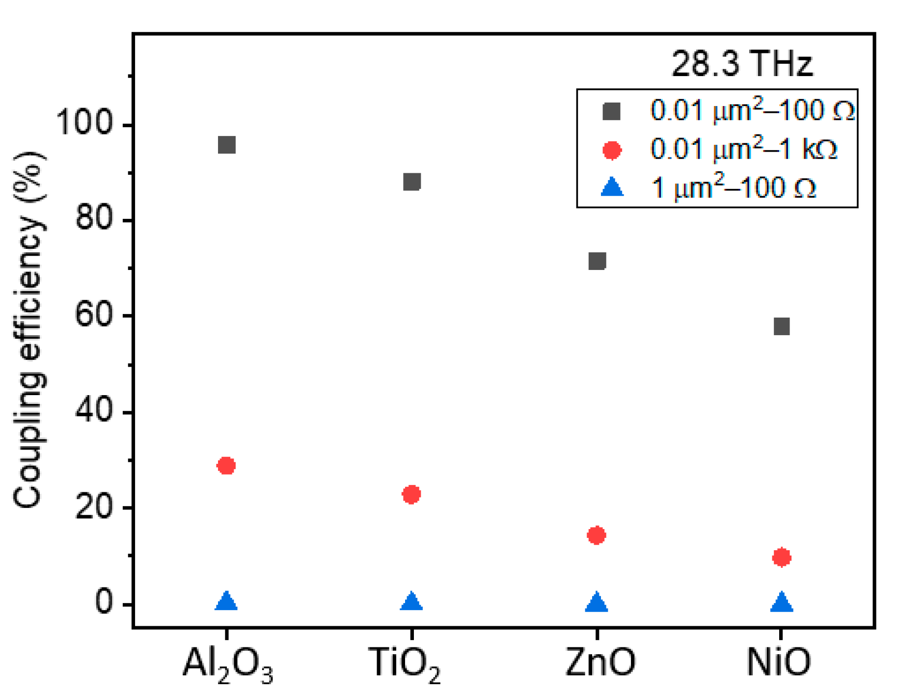
Consider that the antenna has a resistance of 100 Ω for capturing IR radiation and the case of a full impedance match between the diode and the antenna. Furthermore, let us assume the same diode resistance as the antenna. Figure 7 depicts the power coupling efficiency at 28.3 THz of a rectenna that constitutes an MIM diode incorporating four of the most commonly used oxides.
The oxide thickness was fixed at 3 nm in the calculations. The area and the dynamic resistance values were varied between 0.01 and 1 µm2 and 100 Ω–1 kΩ, respectively. The high-frequency permittivity values of oxides (ε∞ = n2, where n is the refractive index) were used for the capacitance calculations [141], as stated in Table 4. As can be seen from Figure 7, the dielectrics Al2O3 and TiO2 come out as strong contenders with the highest coupling efficiency. An interesting observation is that the area seems to be more critical than diode resistance, that is even if the latter is engineered to be 100 Ω, the increase in area to 1 µm2 results in a significant reduction of coupling efficiency.
Needless to say, Figure 7 depicts an ideal case, as fabricating reliable and fully scalable MIM diodes with capacitances of a few atto-farads to operate efficiently at 28.3 THz remains a significant challenge. An emerging novel design approach is an MIM diode engineered with a junction capacitance of ~2 aF at the tip of vertically aligned multiwalled carbon nanotubes (MW-CNTs) (~10 nm in diameter), which act as the antenna [142].
By implementing an Al2O3/ZrO2/Al2O3/ZrO2 quad-insulator laminate structure, asymmetry of 300 and βMAX = 6 A/W has been achieved for the diode and a total conversion efficiency of 3 × 10⁻⁶% for the rectenna [143]. Although very encouraging, the growth of carbon nanotubes must be further improved to obtain a well-ordered network and to favor the amplification of the electromagnetic field structure. Variability and reproducibility are also major challenges considering that the diodes will be incorporated into large arrays to enable the generation of significant power levels.
Other emerging concepts relate to surface plasmon excitation within a MIM device that produces power based on spatial confinement of electron excitation through plasmon absorption [144]. The recent work also proposes MIM-based plasmonic structures that incorporate a nanoslit for IR rectification [145].
4. Conclusions and Outlook
We have presented a review of the state-of-the-art single, double and triple MIM diodes for inclusion in IR nano-rectennas. Typical metals used in MIMs (Ni, Al, Au, Cr and Ti), their skin depths and work function have been summarized. An overview of various oxides, their electron affinity, band gap and permittivity were presented as well as a review of their use in MIM diodes. The lowest zero-bias resistances have been reported for Ni/NiO/Ni (100 Ω), Al/Al2O3/Pt (125 Ω), Al/AlOx/Gr (600 Ω), Au/HfO2/Pt (405 Ω) and Au/CuO/Cu (500 Ω). Apart from the latter diode that exhibits β0 = 2 A/W, generally, these diodes have not been optimized to achieve the high zero-bias responsivity that is required for practical high-frequency operation. Hence, there has been a considerable research effort in engineering a diode with low resistance and high responsivity by utilizing resonant or step tunneling in a double or triple insulator oxide stack. The two oxide contenders for MIM diodes, NiO and Al2O3, have been utilized the most and combined with HfO2, Ta2O5, Nb2O5, ZnO and TiO2. The latter oxide has also been used in combination with Co3O4 and TiOx. The highest zero-bias responsivities of 2.2 and −3.7 A/W have been reported for Ti/TiO2/Co3O4/Co MI2M and Al/Nb2O5/Ta2O5/Al2O3/Al MI3M diodes, respectively, while the lowest zero-bias dynamic resistance of 380 Ω was reported for Ni/NiO/Nb2O5/CrAu. The latest research shows that by modifying the depth and width of the quantum well of a 0.035 μm2 Ni/NiO/AlOx/CrAu resonant tunneling MI2M diode, relatively low R0 = 13 kΩ and high β0 = 0.5 A/W can be achieved simultaneously. The bowtie rectenna based on this diode has been found to have overall power conversion efficiency of 1.7 × 10⁻⁸% and a coupling efficiency of 5.1% when illuminated at 30 THz; the highest achieved to date. Furthermore, defect engineering by nitrogen doping in a Pt/NTiOx/NAlOx/Al diode has led recently to state-of-the-art values of R0 = 36 Ω and β0 = 1.7 A/W. The most recent theoretical work indicates that a Ti/1 nm TiO2/1 nm Nb2O5/Ti diode could achieve even higher β0 = 4.99 A/W and low R0 = 108.6 Ω and, with the diode area of 0.01 μm2, could result in an efficient IR rectenna with a cut-off frequency of 17 THz.
In summary, there is no one optimal solution of metal/oxide stack combination that can yield an efficient MIM rectifier for IR rectenna due to engineering design trade-offs. Rather, several options of MInM are becoming apparent. The latest research points to technological advancements and is focused on the control of oxide thicknesses to sub-nanometer accuracy and oxide stoichiometry by carefully devised fabrication processes, which have resulted in realizing some of the best zero-bias responsivity–resistance optimized diodes. Although there is considerable scope for refinement in device manufacturing, the latest research in this field shows that we are a step closer toward tapping into the infrared spectrum with rectennas based on MIM technology. The race, however, is still on.
Author Contributions
Conceptualization: I.Z.M., S.A., S.B.T., P.R.C. and S.H.; writing—original draft preparation: S.A., S.B.T. and I.Z.M.; figures preparation and calculations—S.B.T. and N.S.; references review—S.A. and S.B.T.; writing—review and editing: I.Z.M., N.S., P.R.C. and S.H. All authors have read and agreed to the published version of the manuscript.
Funding
This research was funded by EPSRC: UK, project number EP/K018930/1 and British Council UGC-UKIERI projects IND/CONT/G/17-18/18 and F.No.184-1/2018(IC).
Institutional Review Board Statement
Not applicable.
Informed Consent Statement
Not applicable.
Data Availability Statement
Not applicable.
Acknowledgments
J.F. Ralph is acknowledged for developing the quantum-mechanical model for prediction of bound states in MInM diodes.
Conflicts of Interest
The authors declare no conflict of interest.
References
- Bailey, R.L. A proposed new concept for a solar-energy converter. J. Eng. Power 1972, 94, 73–77. [Google Scholar] [CrossRef]
- Berland, B. Photovoltaic Technologies Beyond the Horizon: Optical Rectenna Solar Cell; Final Report; National Renewable Energy Lab.: Golden, CO, USA, 2003; NREL/SR-520-33263.
- Brown, W.C. Optimization of the efficiency and other properties of the rectenna element. In Proceedings of the 1976 IEEE-MTT-S International Microwave Symposium, Cherry Hill, NJ, USA, 14–16 June 1976; pp. 142–144. [Google Scholar]
- Moddel, G. Will rectenna solar cells be practical? In Rectenna Sol Cells; Springer: Berlin/Heidelberg, Germany, 2013; pp. 3–24. [Google Scholar]
- Hall, S.; Mitrovic, I.Z.; Sedghi, N.; Yao-chun, C.S.; Huang, Y.; Ralph, J.F. Energy harvesting using THz electronics. In Funct Nanomater Devices Electron Sensors Energy Harvest; Springer: Berlin/Heidelberg, Germany , 2014; pp. 241–265. [Google Scholar]
- Kotter, D.K.; Novack, S.D.; Slafer, W.D.; Pinhero, P.J. Theory and manufacturing processes of solar nanoantenna electromagnetic collectors. J. Sol. Energy Eng. 2010, 132, 11014. [Google Scholar] [CrossRef]
- Hashem, I.E.; Rafat, N.H.; Soliman, E.A. Nanocrescent antenna as a transceiver for optical communication systems. In Proceedings of the 2014 IEEE International Symposium on Electromagnetic Compatibility (EMC), Raleigh, NC, USA, 4–8 August 2014; pp. 39–45. [Google Scholar]
- Gadalla, M.N.; Abdel-Rahman, M.; Shamim, A. Design, optimization and fabrication of a 28.3 THz nano-rectenna for infrared detection and rectification. Sci. Rep. 2014, 4, 1–9. [Google Scholar] [CrossRef] [PubMed]
- Jayaswal, G.; Belkadi, A.; Meredov, A.; Pelz, B.; Moddel, G.; Shamim, A. Optical rectification through an Al2O3 based MIM passive rectenna at 28.3 THz. Mater. Today Energy 2018, 7, 1–9. [Google Scholar] [CrossRef]
- Kausar, A.S.M.Z.; Reza, A.W.; Latef, T.A.; Ullah, M.H.; Karim, M.E. Optical nano antennas: State of the art, scope and challenges as a biosensor along with human exposure to nano-toxicology. Sensors 2015, 15, 8787–8831. [Google Scholar] [CrossRef] [PubMed] [Green Version]
- Gale, W.F.; Totemeier, T.C. Smithells Metals Reference Book; Elsevier: Amsterdam, The Netherlands, 2003. [Google Scholar]
- Nieuwenhuys, B.E.; Bouwman, R.; Sachtler, W.M.H. The changes in work function of group Ib and VIII metals on xenon adsorption, determined by field electron and photoelectron emission. Thin Solid Films 1974, 21, 51–58. [Google Scholar] [CrossRef]
- Greiner, M.T.; Lu, Z.-H. Thin-film metal oxides in organic semiconductor devices: Their electronic structures, work functions and interfaces. NPG Asia Mater. 2013, 5, e55. [Google Scholar] [CrossRef]
- Herner, S.B.; Belkadi, A.; Weerakkody, A.; Pelz, B.; Moddel, G. Responsivity–resistance relationship in MIIM diodes. IEEE J. Photovolt. 2018, 8, 499–504. [Google Scholar] [CrossRef]
- Herner, S.B.; Weerakkody, A.D.; Belkadi, A.; Moddel, G. High performance MIIM diode based on cobalt oxide/titanium oxide. Appl. Phys. Lett. 2017, 110, 223901. [Google Scholar] [CrossRef] [Green Version]
- Michaelson, H.B. The work function of the elements and its periodicity. J. Appl. Phys. 1977, 48, 4729–4733. [Google Scholar] [CrossRef] [Green Version]
- Mitrovic, I.Z.; Weerakkody, A.D.; Sedghi, N.; Ralph, J.F.; Hall, S.; Dhanak, V.R.; Luo, Z.; Beeby, S. Controlled modification of resonant tunneling in metal-insulator-insulator-metal structures. Appl. Phys. Lett. 2018, 112, 012902. [Google Scholar] [CrossRef] [Green Version]
- Alimardani, N.; Conley, J.F., Jr. Step tunneling enhanced asymmetry in asymmetric electrode metal-insulator-insulator-metal tunnel diodes. Appl. Phys. Lett. 2013, 102, 143501. [Google Scholar] [CrossRef] [Green Version]
- Hopkins, B.J.; Rivière, J.C. The work function of polycrystalline tungsten foil. Proc. Phys. Soc. 1963, 81, 590. [Google Scholar] [CrossRef]
- Abdel-Rahman, M.; Issa, K.; Zia, M.F.; Alduraibi, M.; Siraj, M.; Ragheb, A.; Alshebeili, S. High sensitivity vanadium–vanadium pentoxide–aluminium metal–insulator–metal diode. Micro Nano Lett. 2018, 13, 680–683. [Google Scholar] [CrossRef]
- Kretsinger, R.H.; Uversky, V.N.; Permyakov, E.A. Encyclopedia of Metalloproteins; Springer: Berlin/Heidelberg, Germany, 2013. [Google Scholar]
- Matula, R.A. Electrical resistivity of copper, gold, palladium, and silver. J. Phys. Chem. Ref. Data 1979, 8, 1147–1298. [Google Scholar] [CrossRef] [Green Version]
- Radi, H.A.; Rasmussen, J.O. Principles of Physics; Springer: Berlin/Heidelberg, Germany, 2013; Volume 10, pp. 973–978. [Google Scholar]
- Edwards, T.C.; Steer, M.B. Foundations for Microstrip Circuit Design; John Wiley & Sons: Hoboken, NJ, USA, 2016. [Google Scholar]
- Desai, P.D.; Chu, T.K.; James, H.M.; Ho, C.Y. Electrical resistivity of selected elements. J. Phys. Chem. Ref. Data 1984, 13, 1069–1097. [Google Scholar] [CrossRef]
- Maglić, K.D.; Perović, N.L.; Vuković, G.S.; Zeković, L.P. Specific heat and electrical resistivity of niobium measured by subsecond calorimetric technique. Int. J. Thermophys. 1994, 15, 963–972. [Google Scholar] [CrossRef]
- Wilke, I.; Oppliger, Y.; Herrmann, W.; Kneubühl, F.K. Nanometer thin-film Ni-NiO-Ni diodes for 30 THz radiation. Appl. Phys. A 1994, 58, 329–341. [Google Scholar] [CrossRef]
- Fumeaux, C.; Herrmann, W.; Kneubühl, F.K.; Rothuizen, H. Nanometer thin-film Ni-NiO-Ni diodes for detection and mixing of 30 THz radiation. Infrared. Phys. Technol. 1998, 39, 123–183. [Google Scholar] [CrossRef] [Green Version]
- Shriwastava, S.; Tripathi, C.C. Metal–insulator–metal diodes: A potential high frequency rectifier for rectenna application. J. Electron. Mater. 2019, 48, 2635–2652. [Google Scholar] [CrossRef]
- Alimardani, N.; Conley, J.F., Jr. Enhancing metal-insulator-insulator-metal tunnel diodes via defect enhanced direct tunneling. Appl. Phys. Lett. 2014, 105, 082902. [Google Scholar] [CrossRef] [Green Version]
- Cowell, E.W., III; Wager, J.F.; Gibbons, B.J.; Keszler, D.A. Amorphous Multi-Component Metallic Thin Films for Electronic Devices. U.S. Patent No 8,436,337, May, 2013. [Google Scholar]
- Wu, H.; Wang, L.-S. A study of nickel monoxide (NiO), nickel dioxide (ONiO), and Ni(O2) complex by anion photoelectron spectroscopy. J. Chem. Phys. 1997, 107, 16–21. [Google Scholar] [CrossRef] [Green Version]
- Robertson, J. Band offsets, Schottky barrier heights, and their effects on electronic devices. J. Vac. Sci. Technol. A 2013, 31, 50821. [Google Scholar] [CrossRef]
- Huang, M.L.; Chang, Y.C.; Chang, C.H.; Lin, T.D.; Kwo, J.; Wu, T.B.; Hong, M. Energy-band parameters of atomic-layer-deposition Al2O3/InGaAs heterostructure. Appl. Phys. Lett. 2006, 89, 012903. [Google Scholar] [CrossRef]
- Liu, Z.; Liu, Y.; Wang, X.; Li, W.; Zhi, Y.; Wang, X.; Li, P.; Tang, W. Energy-band alignments at ZnO/Ga2O3 and Ta2O5/Ga2O3 heterointerfaces by X-ray photoelectron spectroscopy and electron affinity rule. J. Appl. Phys. 2019, 126, 045707. [Google Scholar] [CrossRef] [Green Version]
- Robertson, J. Band offsets of wide-band-gap oxides and implications for future electronic devices. J. Vac. Sci. Technol. B 2000, 18, 1785–1791. [Google Scholar] [CrossRef]
- Koffyberg, F.P.; Benko, F.A. A photoelectrochemical determination of the position of the conduction and valence band edges of p-type CuO. J. Appl. Phys. 1982, 53, 1173–1177. [Google Scholar] [CrossRef]
- Alimardani, N.; King, S.W.; French, B.L.; Tan, C.; Lampert, B.P.; Conley, J.F., Jr. Investigation of the impact of insulator material on the performance of dissimilar electrode metal-insulator-metal diodes. J. Appl. Phys. 2014, 116, 024508. [Google Scholar] [CrossRef] [Green Version]
- Gutsev, G.L.; Jena, P.; Zhai, H.-J.; Wang, L.-S. Electronic structure of chromium oxides, CrOn− and CrOn (n = 1–5) from photoelectron spectroscopy and density functional theory calculations. J. Chem. Phys. 2001, 115, 7935–7944. [Google Scholar] [CrossRef]
- Miura, A.; Uraoka, Y.; Fuyuki, T.; Yoshii, S.; Yamashita, I. Floating nanodot gate memory fabrication with biomineralized nanodot as charge storage node. J. Appl. Phys. 2008, 103, 74503. [Google Scholar] [CrossRef]
- Monaghan, S.; Hurley, P.K.; Cherkaoui, K.; Negara, M.A.; Schenk, A. Determination of electron effective mass and electron affinity in HfO2 using MOS and MOSFET structures. Solid State Electron. 2009, 53, 438–444. [Google Scholar] [CrossRef] [Green Version]
- Xing, K.; Zhang, S.; Tsai, A.; Xiao, H.; Creedon, D.L.; Yianni, S.A.; McCallum, J.C.; Pakes, C.I.; Qi, D.-C. High-electron-affinity oxide V2O5 enhances surface transfer doping on hydrogen-terminated diamond. Diam. Relat. Mater. 2020, 108, 107865. [Google Scholar] [CrossRef]
- Afanas’ev, V.V.; Shamuilia, S.; Badylevich, M.; Stesmans, A.; Edge, L.F.; Tian, W.; Schlom, D.G.; Lopes, J.M.J.; Roeckerath, M.; Schubert, J. Electronic structure of silicon interfaces with amorphous and epitaxial insulating oxides: Sc2O3, Lu2O3, LaLuO3. Microelectron. Eng. 2007, 84, 2278–2281. [Google Scholar] [CrossRef]
- Hosseini, S.; Vahedpour, M.; Shaterian, M.; Rezvani, M.A. Investigation of structural and optoelectronic properties of Sc2O3 nanoclusters: A DFT study. Phys. Chem. Res. 2018, 6, 493–504. [Google Scholar]
- Weerakkody, A.; Belkadi, A.; Moddel, G. Nonstoichiometric nanolayered Ni/NiO/Al2O3/CrAu Metal-Insulator-Metal infrared rectenna. ACS Appl. Nano Mater. 2021, 4, 2470–2475. [Google Scholar] [CrossRef]
- Kurmaev, E.Z.; Wilks, R.G.; Moewes, A.; Finkelstein, L.D.; Shamin, S.N.; Kuneš, J. Oxygen x-ray emission and absorption spectra as a probe of the electronic structure of strongly correlated oxides. Phys. Rev. B 2008, 77, 165127. [Google Scholar] [CrossRef] [Green Version]
- Mitrovic, I.Z.; Althobaiti, M.; Weerakkody, A.D.; Dhanak, V.R.; Linhart, W.M.; Veal, T.D.; Sedghi, N.; Hall, S.; Chalker, P.R.; Tsoutsou, D.; et al. Ge interface engineering using ultra-thin La2O3 and Y2O3 films: A study into the effect of deposition temperature. J. Appl. Phys. 2014, 115, 114102. [Google Scholar] [CrossRef] [Green Version]
- Sun, S.-M.; Liu, W.-J.; Xiao, Y.-F.; Huan, Y.-W.; Liu, H.; Ding, S.-J.; Zhang, D.W. Investigation of energy band at atomic-layer-deposited ZnO/β-Ga2O3 heterojunctions. Nanoscale. Res. Lett. 2018, 13, 1–6. [Google Scholar] [CrossRef] [PubMed]
- Aarik, J.; Aidla, A.; Kiisler, A.-A.; Uustare, T.; Sammelselg, V. Effect of crystal structure on optical properties of TiO2 films grown by atomic layer deposition. Thin Solid Films 1997, 305, 270–273. [Google Scholar] [CrossRef]
- Valladares, L.D.L.S.; Salinas, D.H.; Dominguez, A.B.; Najarro, D.A.; Khondaker, S.I.; Mitrelias, T.; Barnes, C.H.W.; Aguiar, J.A.; Majima, Y. Crystallization and electrical resistivity of Cu2O and CuO obtained by thermal oxidation of Cu thin films on SiO2/Si substrates. Thin Solid Films 2012, 520, 6368–6374. [Google Scholar] [CrossRef]
- Weerakkody, A.D.; Sedghi, N.; Mitrovic, I.Z.; Van Zalinge, H.; Noureddine, I.N.; Hall, S.; Wrench, J.S.; Chalker, P.R.; Phillips, L.J.; Treharne, R.; et al. Enhanced low voltage nonlinearity in resonant tunneling metal–insulator–insulator–metal nanostructures. Microelectron. Eng. 2015, 147, 298–301. [Google Scholar] [CrossRef]
- Abdullah, M.M.; Rajab, F.M.; Al-Abbas, S.M. Structural and optical characterization of Cr2O3 nanostructures: Evaluation of its dielectric properties. AIP Adv. 2014, 4, 27121. [Google Scholar] [CrossRef]
- Singh, J.; Verma, V.; Kumar, R.; Kumar, R. Structural, optical and electrical characterization of epitaxial Cr2O3 thin film deposited by PLD. Mater. Res. Express 2019, 6, 106406. [Google Scholar] [CrossRef]
- Shinde, V.R.; Mahadik, S.B.; Gujar, T.P.; Lokhande, C.D. Supercapacitive cobalt oxide (Co3O4) thin films by spray pyrolysis. Appl. Surf. Sci. 2006, 252, 7487–7492. [Google Scholar] [CrossRef]
- Thiagarajan, S.; Thaiyan, M.; Ganesan, R. Physical property exploration of highly oriented V2O5 thin films prepared by electron beam evaporation. New J. Chem. 2015, 39, 9471–9479. [Google Scholar] [CrossRef]
- Mitrovic, I.Z.; Weerakkody, A.D.; Sedghi, N.; Hall, S.; Ralph, J.F.; Wrench, J.S.; Chalker, P.R.; Luo, Z.; Beeby, S. Tunnel-barrier rectifiers for optical nantennas. ECS Trans. 2016, 72, 287. [Google Scholar] [CrossRef] [Green Version]
- Sollner, T.; Goodhue, W.D.; Tannenwald, P.E.; Parker, C.D.; Peck, D.D. Resonant tunneling through quantum wells at frequencies up to 2.5 THz. Appl. Phys. Lett. 1983, 43, 588–590. [Google Scholar] [CrossRef] [Green Version]
- Maraghechi, P.; Foroughi-Abari, A.; Cadien, K.; Elezzabi, A.Y. Enhanced rectifying response from metal-insulator-insulator-metal junctions. Appl. Phys. Lett. 2011, 99, 253503. [Google Scholar] [CrossRef]
- Abdel-Rahman, M.R.; Gonzalez, F.J.; Boreman, G.D. Antenna-coupled metal-oxide-metal diodes for dual-band detection at 92.5 GHz and 28 THz. Electron. Lett. 2004, 40, 116–118. [Google Scholar] [CrossRef] [Green Version]
- Hobbs, P.C.D.; Laibowitz, R.B.; Libsch, F.R.; LaBianca, N.C.; Chiniwalla, P.P. Efficient waveguide-integrated tunnel junction detectors at 1.6 µm. Opt. Express. 2007, 15, 16376–16389. [Google Scholar] [CrossRef]
- Choi, K.; Yesilkoy, F.; Ryu, G.; Cho, S.H.; Goldsman, N.; Dagenais, M.; Peckerar, M. A focused asymmetric metal–insulator–metal tunneling diode: Fabrication, DC characteristics and RF rectification analysis. IEEE Trans Electron Devices 2011, 58, 3519–3528. [Google Scholar] [CrossRef]
- Hoofring, A.B.; Kapoor, V.J.; Krawczonek, W. Submicron nickel-oxide-gold tunnel diode detectors for rectennas. J. Appl. Phys. 1989, 66, 430–437. [Google Scholar] [CrossRef]
- Azad, I.; Ram, M.K.; Goswami, D.Y.; Stefanakos, E. Fabrication and characterization of NiO based metal− insulator− metal diode using Langmuir-Blodgett method for high frequency rectification. AIP Adv. 2018, 8, 45219. [Google Scholar] [CrossRef]
- Zhuang, C.; Wang, L.; Dai, Z.; Yang, D. High frequency Ni-NiO-Ag metal-insulator-metal tunnel diodes fabricated via anodic aluminum oxide templates. ECS Solid State Lett. 2015, 4, P39. [Google Scholar] [CrossRef]
- Esfandiari, P.; Bernstein, G.; Fay, P.; Porod, W.; Rakos, B.; Zarandy, A.; Berland, B.; Boloni, L.; Boreman, G.; Lail, B.; et al. Tunable antenna-coupled metal-oxide-metal (MOM) uncooled IR detector. Infrared. Technol. Appl. XXXI 2005, 5783, 470. [Google Scholar]
- Krishnan, S.; La Rosa, H.; Stefanakos, E.; Bhansali, S.; Buckle, K. Design and development of batch fabricatable metal–insulator–metal diode and microstrip slot antenna as rectenna elements. Sens. Actuators A Phys. 2008, 142, 40–47. [Google Scholar] [CrossRef]
- Krishnan, S.; Stefanakos, E.; Bhansali, S. Effects of dielectric thickness and contact area on current-voltage characteristics of thin film metal-insulator-metal diodes. Thin Solid Films 2008, 516, 2244–2250. [Google Scholar] [CrossRef]
- Zhang, S.; Wang, L.; Xu, C.; Li, D.; Chen, L.; Yang, D. Fabrication of Ni-NiO-Cu metal-insulator-metal tunnel diodes via anodic aluminum oxide templates. ECS Solid State Lett. 2012, 2, Q1. [Google Scholar] [CrossRef]
- Kaur, A.; Chahal, P. RF characterization of NiO and TiO2 based metal-insulator-metal (MIM) diodes on flexible substrates. IEEE Access 2018, 6, 55653–55660. [Google Scholar] [CrossRef]
- Bareis, M.; Tiwari, B.N.; Hochmeister, A.; Jegert, G.; Zschieschang, U.; Klauk, H.; Fabel, B.; Scarpa, G.; Koblmüller, G.; Bernstein, G.H.; et al. Nano antenna array for terahertz detection. IEEE Trans Microw. Theory Tech. 2011, 59, 2751–2757. [Google Scholar]
- Bean, J.A.; Tiwari, B.; Bernstein, G.H.; Fay, P.; Porod, W. Thermal infrared detection using dipole antenna-coupled metal-oxide-metal diodes. J. Vac. Sci. Technol. B 2009, 27, 11–14. [Google Scholar] [CrossRef]
- Kinzel, E.C.; Brown, R.L.; Ginn, J.C.; Lail, B.A.; Slovick, B.A.; Boreman, G.D. Design of an MOM diode-coupled frequency-selective surface. Microw. Opt. Technol. Lett. 2013, 55, 489–493. [Google Scholar] [CrossRef]
- Bhatt, K.; Kumar, S.; Tripathi, C.C. Highly sensitive Al/Al2O3/Ag MIM diode for energy harvesting applications. AEU Int. J. Electron. Commun. 2019, 111, 152925. [Google Scholar] [CrossRef]
- Shriwastava, S.; Arya, D.S.; Sharma, S.; Singh, K.; Singh, P.; Tripathi, C.C. A laser patterned zero bias Au/Al2O3/Mo metal-insulator-metal diode rectifier for RF detection. Solid State Electron. 2020, 171, 107870. [Google Scholar] [CrossRef]
- Tekin, S.B.; Weerakkody, A.D.; Sedghi, N.; Hall, S.; Werner, M.; Wrench, J.S.; Chalker, P.R.; Mitrovic, I.Z. Single and triple insulator Metal-Insulator-Metal diodes for infrared rectennas. Solid State Electron. 2021, 185, 108096. [Google Scholar] [CrossRef]
- Hobbs, P.C.D.; Laibowitz, R.B.; Libsch, F.R. Ni–NiO–Ni tunnel junctions for terahertz and infrared detection. Appl. Opt. 2005, 44, 6813–6822. [Google Scholar] [CrossRef] [Green Version]
- Bean, J.A.; Weeks, A.; Boreman, G.D. Performance optimization of antenna-coupled Al/AlOx/Pt tunnel diode infrared detectors. IEEE J. Quantum Electron. 2010, 47, 126–135. [Google Scholar] [CrossRef]
- Dodd, L.E.; Wood, D.; Gallant, A.J. Optimizing MOM diode performance via the oxidation technique. In Sensors; IEEE: New York, NY, USA, 2011; pp. 176–179. [Google Scholar]
- Urcuyo, R.; Duong, D.L.; Jeong, H.Y.; Burghard, M.; Kern, K. High performance graphene–oxide–metal diode through bias-induced barrier height modulation. Adv. Electron. Mater. 2016, 2, 1–6. [Google Scholar] [CrossRef]
- Singh, A.; Ratnadurai, R.; Kumar, R.; Krishnan, S.; Emirov, Y.; Bhansali, S. Fabrication and current–voltage characteristics of NiOx/ZnO based MIIM tunnel diode. Appl. Surf. Sci. 2015, 334, 197–204. [Google Scholar] [CrossRef]
- Khan, A.A.; Jayaswal, G.; Gahaffar, F.A.; Shamim, A. Metal-insulator-metal diodes with sub-nanometre surface roughness for energy-harvesting applications. Microelectron. Eng. 2017, 181, 34–42. [Google Scholar] [CrossRef] [Green Version]
- Azad, I.; Ram, M.K.; Goswami, D.Y.; Stefanakos, E. Fabrication and characterization of ZnO Langmuir–Blodgett film and its use in metal–insulator–metal tunnel diode. Langmuir 2016, 32, 8307–8314. [Google Scholar] [CrossRef]
- Zia, M.F.; Abdel-Rahman, M.R.; Al-Khalli, N.F.; Debbar, N.A. Fabrication and characterization of vanadium/vanadium pentoxide/vanadium (V/V2O5/V) tunnel junction diodes. Acta Phys. Pol. A 2015, 127, 1289–1291. [Google Scholar] [CrossRef]
- Dagenais, M.; Choi, K.; Yesilkoy, F.; Chryssis, A.N.; Peckerar, M.C. Solar spectrum rectification using nano-antennas and tunneling diodes. In Optoelectronic Integrated Circuits XII; International Society for Optics and Photonics: Bellingham, WA, USA, 2010; p. 76050E. [Google Scholar]
- Choi, K.; Yesilkoy, F.; Chryssis, A.; Dagenais, M.; Peckerar, M. New process development for planar-type CIC tunneling diodes. IEEE Electron. Device Lett. 2010, 31, 809–811. [Google Scholar] [CrossRef]
- Periasamy, P.; Berry, J.J.; Dameron, A.A.; Bergeson, J.D.; Ginley, D.S.; O’Hayre, R.P. Fabrication and characterization of MIM diodes based on Nb/Nb2O5 via a rapid screening technique. Adv. Mater. 2011, 23, 3080–3085. [Google Scholar] [CrossRef] [PubMed]
- Chin, M.L.; Periasamy, P.; O’Regan, T.P.; Amani, M.; Tan, C.; O’Hayre, R.P.; Berry, J.J.; Osgood III, R.M.; Parilla, P.A.; Ginley, D.S.; et al. Planar metal–insulator–metal diodes based on the Nb/Nb2O5/X material system. J. Vac. Sci. Technol. B 2013, 31, 051204. [Google Scholar] [CrossRef]
- Inac, M.; Shafique, A.; Ozcan, M.; Gurbuz, Y. Device characteristics of antenna-coupled metal-insulator-metal diodes (rectenna) using Al2O3, TiO2, and Cr2O3 as insulator layer for energy harvesting applications. In Thin Film Sol Energy Technol VII; International Society for Optics and Photonics: Bellingham, WA, USA, 2015; p. 95610M. [Google Scholar]
- Aldrigo, M.; Dragoman, M.; Modreanu, M.; Povey, I.; Iordanescu, S.; Vasilache, D.; Dinescu, A.; Shanawani, M.; Masotti, D. Harvesting electromagnetic energy in the V-band using a rectenna formed by a bow tie integrated with a 6-nm-thick Au/HfO2/Pt Metal–Insulator–Metal diode. IEEE Trans Electron. Devices 2018, 65, 2973–2980. [Google Scholar] [CrossRef]
- Almalki, S.; Tekin, S.B.; Sedghi, N.; Hall, S.; Mitrovic, I.Z. Applicability of Sc2O3 versus Al2O3 in MIM rectifiers for IR rectenna. Solid State Electron. 2021, 184, 108082. [Google Scholar] [CrossRef]
- Grover, S.; Moddel, G. Engineering the current–voltage characteristics of metal–insulator–metal diodes using double-insulator tunnel barriers. Solid State Electron. 2012, 67, 94–99. [Google Scholar] [CrossRef]
- Sedghi, N.; Ralph, J.F.; Mitrovic, I.Z.; Chalker, P.R.; Hall, S. Electron trapping at the high-κ/GeO2 interface: The role of bound states. Appl. Phys. Lett. 2013, 102, 092103. [Google Scholar] [CrossRef]
- Sedghi, N.; Zhang, J.W.; Ralph, J.F.; Huang, Y.; Mitrovic, I.Z.; Hall, S. Towards rectennas for solar energy harvesting. In Proceedings of the 2013 European Solid-State Device Research Conference (ESSDERC), Bucharest, Romania, 16–20 September 2013; pp. 131–134. [Google Scholar]
- Mistry, K.; Yavuz, M.; Musselman, K.P. Simulated electron affinity tuning in metal-insulator-metal (MIM) diodes. J. Appl. Phys. 2017, 121, 184504. [Google Scholar] [CrossRef]
- Weerakkody, D.A.D.C. Engineered High-K Oxides. Ph.D. Thesis, University of Liverpool, Liverpool, UK, 2016. [Google Scholar]
- Noureddine, I.N.; Sedghi, N.; Mitrovic, I.Z.; Hall, S. Barrier tuning of atomic layer deposited Ta2O5 and Al2O3 in double dielectric diodes. J. Vac. Sci. Technol. B 2017, 35, 01A117. [Google Scholar] [CrossRef] [Green Version]
- Belkadi, A.; Weerakkody, A.; Moddel, G. Demonstration of resonant tunneling effects in metal-double-insulator-metal (MI2M) diodes. Nat. Commun. 2021, 12, 1–6. [Google Scholar] [CrossRef]
- Pelz, B.; Moddel, G. Demonstration of distributed capacitance compensation in a metal-insulator-metal infrared rectenna incorporating a traveling-wave diode. J. Appl. Phys. 2019, 125, 234502. [Google Scholar] [CrossRef] [Green Version]
- Elsharabasy, A.Y.; Negm, A.S.; Bakr, M.H.; Deen, M.J. Global optimization of rectennas for IR energy harvesting at 10.6 μm. IEEE J. Photovolt. 2019, 9, 232–239. [Google Scholar] [CrossRef]
- Matsuura, D.; Shimizu, M.; Yugami, H. High-current density and high-asymmetry MIIM diode based on oxygen-non-stoichiometry controlled homointerface structure for optical rectenna. Sci. Rep. 2019, 9, 1–7. [Google Scholar]
- Alshehri, A.H.; Shahin, A.; Mistry, K.; Ibrahim, K.H.; Yavuz, M.; Musselman, K.P. Metal-Insulator-Insulator-Metal diodes with responsivities greater than 30 AW−1 based on nitrogen-doped TiOx and AlOx insulator layers. Adv. Electron. Mater. 2021, 2021, 2100467. [Google Scholar] [CrossRef]
- Noureddine, I.N.; Sedghi, N.; Wrench, J.; Chalker, P.; Mitrovic, I.Z.; Hall, S. Fabrication and modelling of MInM diodes with low turn-on voltage. Solid State Electron. 2021, 184, 108053. [Google Scholar] [CrossRef]
- Elsharabasy, A.Y.; Bakr, M.H.; Deen, M.J. Towards an optimal MIIM diode for rectennas at 10.6 μml MIIM diode for rectennas at 10.6 μm. Results Mater. 2021, 11, 100204. [Google Scholar] [CrossRef]
- Maraghechi, P.; Foroughi-Abari, A.; Cadien, K.; Elezzabi, A.Y. Observation of resonant tunneling phenomenon in metal-insulator-insulator-insulator-metal electron tunnel devices. Appl. Phys. Lett. 2012, 100, 113503. [Google Scholar] [CrossRef]
- Xie, L.Y.; Xiao, D.Q.; Pei, J.X.; Huo, J.; Wu, X.; Liu, W.J.; Ding, S.J. Growth, physical and electrical characterization of nickel oxide thin films prepared by plasma-enhanced atomic layer deposition using nickelocene and oxygen precursors. Mater. Res. Express. 2020, 7, 046401. [Google Scholar] [CrossRef]
- Cho, W.; Lee, S.S.; Chung, T.M.; Kim, C.G.; An, K.S.; Ahn, J.P.; Lee, J.Y.; Lee, W.W.; Hwang, J.H. Nonvolatile memory effects of NiO layers embedded in Al2O3 high-k dielectrics using atomic layer deposition. Electrochem. Solid State Lett. 2010, 13, 6–9. [Google Scholar] [CrossRef]
- Kashir, A.; Jeong, H.W.; Lee, G.H.; Mikheenko, P.; Jeong, Y.H. Dielectric properties of strained nickel oxide thin films. J. Korean Phys. Soc. 2019, 74, 984–988. [Google Scholar] [CrossRef]
- Thacker, Z.; Pinhero, P.J. Terahertz spectroscopy of candidate oxides in MIM diodes for terahertz detection. IEEE Trans. Terahertz. Sci. Technol. 2016, 6, 414–419. [Google Scholar] [CrossRef]
- Abdel-Rahman, M.R.; Monacelli, B.; Weeks, A.R.; Zummo, G.; Boreman, G.D. Design, fabrication, and characterization of antenna-coupled metal-oxide-metal diodes for dual-band detection. Opt. Eng. 2005, 44, 066401. [Google Scholar] [CrossRef]
- Das, P.; Jones, L.A.H.; Gibbon, J.T.; Dhanak, V.R.; Partida-Manzanera, T.; Roberts, J.W.; Potter, R.; Chalker, P.R.; Cho, S.J.; Thayne, I.; et al. Band line-up investigation of atomic layer deposited TiAlO and GaAlO on GaN. ECS J. Solid State Sci. Technol. 2020, 9, 63003. [Google Scholar] [CrossRef]
- Groner, M.D.; Elam, J.W.; Fabreguette, F.H.; George, S.M. Electrical characterization of thin Al2O3 films grown by atomic layer deposition on silicon and various metal substrates. Thin Solid Films 2002, 413, 186–197. [Google Scholar] [CrossRef]
- Argall, F.; Jonscher, A.K. Dielectric properties of thin films of aluminium oxide and silicon oxide. Thin Solid Films 1968, 2, 185–210. [Google Scholar] [CrossRef]
- Smith, S.W.; McAuliffe, K.G.; Conley, J.F., Jr. Atomic layer deposited high-k nanolaminate capacitors. Solid State Electron. 2010, 54, 1076–1082. [Google Scholar] [CrossRef]
- Wilk, G.D.; Wallace, R.M.; Anthony, J. High-κ gate dielectrics: Current status and materials properties considerations. J. Appl. Phys. 2001, 89, 5243–5275. [Google Scholar] [CrossRef]
- Ye, P.D.; Yang, B.; Ng, K.K.; Bude, J.; Wilk, G.D.; Halder, S.; Hwang, J.C.M. GaN metal-oxide-semiconductor high-electron-mobility-transistor with atomic layer deposited Al2O3 as gate dielectric. Appl. Phys. Lett. 2005, 86, 063501. [Google Scholar] [CrossRef] [Green Version]
- Yota, J.; Shen, H.; Ramanathan, R. Characterization of atomic layer deposition HfO2, Al2O3, and plasma-enhanced chemical vapor deposition Si3N4 as metal–insulator–metal capacitor dielectric for GaAs HBT technology. J. Vac. Sci. Technol. A 2013, 31, 01A134. [Google Scholar] [CrossRef] [Green Version]
- Rajab, K.Z.; Naftaly, M.; Linfield, E.H.; Nino, J.C.; Arenas, D.; Tanner, D.; Mittra, R.; Lanagan, M. Broadband dielectric characterization of aluminum oxide (Al2O3). J. Microelectron. Electron. Packag. 2008, 5, 2–7. [Google Scholar] [CrossRef]
- Kim, Y.; Yi, M.; Kim, B.G.; Ahn, J. Investigation of THz birefringence measurement and calculation in Al2O3 and LiNbO3. Appl. Opt. 2011, 50, 2906–2910. [Google Scholar] [CrossRef]
- Kischkat, J.; Peters, S.; Gruska, B.; Semtsiv, M.; Chashnikova, M.; Klinkmüller, M.; Fedosenko, O.; Machulik, S.; Aleksandrova, A.; Monastyrskyi, G.; et al. Mid-infrared optical properties of thin films of aluminum oxide, titanium dioxide, silicon dioxide, aluminum nitride, and silicon nitride. Appl. Opt. 2012, 51, 6789–6798. [Google Scholar] [CrossRef] [PubMed]
- Hutson, A.R. Hall effect studies of doped zinc oxide single crystals. Phys Rev. 1957, 108, 222–230. [Google Scholar] [CrossRef]
- Langton, N.H.; Matthews, D. The dielectric constant of zinc oxide over a range of frequencies. Br. J. Appl. Phys. 1958, 9, 453. [Google Scholar] [CrossRef]
- Querry, M.R. Optical Constants, Report No.AD-A158 623, CR-85034:1–413. 1985. Available online: https://apps.dtic.mil/dtic/tr/fulltext/u2/a158623.pdf (accessed on 3 September 2021).
- Stamate, M.D. Dielectric properties of TiO2 thin films deposited by a DC magnetron sputtering system. Thin Solid Films 2000, 372, 246–249. [Google Scholar] [CrossRef]
- Rausch, N.; Burte, E.P. Thin TiO2 films prepared by low pressure chemical vapor deposition. J. Electrochem. Soc. 1993, 140, 145–149. [Google Scholar] [CrossRef]
- Shvets, V.A.; Kruchinin, V.N.; Gritsenko, V.A. Dispersion of the refractive index in high-k dielectrics. Opt. Spectrosc. 2017, 123, 728–732. [Google Scholar] [CrossRef]
- Andrés, E.S.; Toledano-Luque, M.; del Prado, A.; Navacerrada, A.; Mártil, I.; González-Díaz, G.; Bohne, W.; Röhrich, J.; Strub, E. Physical properties of high pressure reactively sputtered TiO2. J. Vac. Sci. Technol. A 2005, 23, 1523–1530. [Google Scholar] [CrossRef]
- Takeuchi, M.; Itoh, T.; Nagasaka, H. Dielectric properties of sputtered TiO2 films. Thin Solid Films 1978, 51, 83–88. [Google Scholar] [CrossRef]
- Matsumoto, N.; Hosokura, T.; Kageyama, K.; Takagi, H.; Sakabe, Y.; Hangyo, M. Analysis of dielectric response of TiO2 in terahertz frequency region by general harmonic oscillator model. Jpn. J. Appl. Phys. 2008, 47, 7725–7728. [Google Scholar] [CrossRef]
- Wang, D.D.; Zhou, F.Z.; Cao, J.X.; Li, L.B.; Li, G.L. Impact of Cu2O doping on high dielectric properties of CuO ceramics. Current Appl. Phys. 2017, 17, 781–784. [Google Scholar] [CrossRef]
- Parretta, A.; Jayaraj, M.K.; Di Nocera, A.; Loreti, S.; Quercia, L.; Agati, A. Electrical and optical properties of copper oxide films prepared by reactive RF magnetron sputtering. Phys. Status Solidi Appl. Res. 1996, 155, 399–404. [Google Scholar] [CrossRef]
- Bright, T.J.; Watjen, J.I.; Zhang, Z.M.; Muratore, C.; Voevodin, A.A.; Koukis, D.I.; Tanner, D.B.; Arenas, D.J. Infrared optical properties of amorphous and nanocrystalline Ta2O5 thin films. J. Appl. Phys. 2013, 114, 083515. [Google Scholar] [CrossRef]
- Dube, D.C.; Agrawal, D.; Agrawal, S.; Roy, R. High temperature dielectric study of Cr2O3 in microwave region. Appl. Phys. Lett. 2007, 90, 124105. [Google Scholar] [CrossRef]
- Fang, P.H.; Brower, W.S. Dielectric constant of Cr2O3 crystals. Phys. Rev. 1963, 129, 1561. [Google Scholar] [CrossRef]
- Wheeler, V.D.; Shahin, D.I.; Tadjer, M.J.; Eddy, C.R., Jr. Band alignments of atomic layer deposited ZrO2 and HfO2 high-k dielectrics with (-201) β-Ga2O3. ECS J. Solid State Sci. Technol. 2016, 6, Q3052. [Google Scholar] [CrossRef]
- Conley, J.F.; Alimardani, N. Impact of electrode roughness on metal-insulator-metal (MIM) diodes and step tunneling in nanolaminate tunnel barrier metal-insulator-insulator-metal (MIIM) diodes. In Rectenna Solar Cells; Springer: Berlin/Heidelberg, Germany, 2013; pp. 111–134. [Google Scholar]
- Thomas, B.; Jayalekshmi, S. Dielectric properties of vanadium pentoxide thin films in the audio frequency range. J. Non Cryst. Solids 1989, 113, 65–72. [Google Scholar] [CrossRef]
- Belosludtsev, A.; Yakimov, Y.; Mroczyński, R.; Stanionytė, S.; Skapas, M.; Buinovskis, D.; Kyžas, N. Effect of annealing on optical, mechanical, electrical properties and structure of scandium oxide films. Phys. Status Solidi 2019, 216, 1900122. [Google Scholar] [CrossRef]
- Kim, J.; Mehandru, R.; Luo, B.; Ren, F.; Gila, B.P.; Onstine, A.H.; Abernathy, C.R.; Pearton, S.J.; Irokawa, Y. Inversion behavior in Sc2O3/GaN gated diodes. Appl. Phys. Lett. 2002, 81, 373–375. [Google Scholar] [CrossRef]
- Yakovkina, L.V.; Smirnova, T.P.; Borisov, V.O.; Kichai, V.N.; Kaichev, V.V. Synthesis and properties of dielectric (HfO2)1−x(Sc2O3)x films. Inorg. Mater. 2013, 49, 172–178. [Google Scholar] [CrossRef]
- Bareiß, M.; Kälblein, D.; Jirauschek, C.; Exner, A.; Pavlichenko, I.; Lotsch, B.; Zschieschang, U.; Klauk, H.; Scarpa, G.; Fabel, B.; et al. Ultra-thin titanium oxide. Appl. Phys. Lett. 2012, 101, 083113. [Google Scholar] [CrossRef] [Green Version]
- Hannachi, L.; Bouarissa, N. Band parameters for cadmium and zinc chalcogenide compounds. Phys. B Condens. Matter. 2009, 404, 3650–3654. [Google Scholar] [CrossRef]
- Sharma, A.; Singh, V.; Bougher, T.L.; Cola, B.A. A carbon nanotube optical rectenna. Nat. Nanotechnol. 2015, 10, 1027–1032. [Google Scholar] [CrossRef]
- Anderson, E.C.; Cola, B.A. Photon-assisted tunneling in carbon nanotube optical rectennas: Characterization and modeling. ACS Appl. Electron. Mater. 2019, 1, 692–700. [Google Scholar] [CrossRef]
- Wang, F.; Melosh, N.A. Plasmonic energy collection through hot carrier extraction. Nano Lett. 2011, 11, 5426–5430. [Google Scholar] [CrossRef] [PubMed]
- Ogawa, S.; Fukushima, S.; Okuda, S.; Shimatani, M. Graphene nanoribbon photogating for graphene-based infrared photodetectors. In Infrared Technology and Applications XLVII; International Society for Optics and Photonics: Bellingham, WA, USA, 2021; p. 117411H. [Google Scholar]
Figure 1.
(a) Schematic of a rectenna device and (b) its equivalent circuit.

Figure 2.
(a) Skin depth and (b) work function [11,12,13,14,15,16,17,18,19,20] for typical metals used in a rectenna.

Figure 3.
(a) Electron affinity and (b) band gap of typical oxides for MIM diodes. Full details are provided in Table 1.
Figure 3.
(a) Electron affinity and (b) band gap of typical oxides for MIM diodes. Full details are provided in Table 1.

Figure 4.
(a) Responsivity and (b) dynamic resistance for various MIM diodes. Full details are summarized in Table 2.
Figure 4.
(a) Responsivity and (b) dynamic resistance for various MIM diodes. Full details are summarized in Table 2.

Figure 5.
Schematics of band alignment for: (a) MI2M diode under positive bias on metal 2 showing bound states in a quantum well and conditions for resonant tunneling to occur; (b) MI3M diode under zero bias, depicting existence of bound states in a deep quantum well; (c) MI2M diode under negative bias on metal 2 and conditions of step tunneling.

Figure 6.
(a) Responsivity and (b) zero-bias dynamic resistance for MInM diodes. For full details, please see Table 3.
Figure 6.
(a) Responsivity and (b) zero-bias dynamic resistance for MInM diodes. For full details, please see Table 3.

Figure 7.
Calculated coupling efficiency for the MIM rectenna device at 28.3 THz using 3 nm oxide thickness and dynamic permittivity values as stated in Table 4.
Figure 7.
Calculated coupling efficiency for the MIM rectenna device at 28.3 THz using 3 nm oxide thickness and dynamic permittivity values as stated in Table 4.


Table 1.
Physical properties of metals and oxides: work function, electron affinity and band gap.
| Metal | Work Function (eV) | Oxide | Electron Affinity, χ (eV) | Band Gap (eV) |
|---|---|---|---|---|
| Ni | 4.9 [11,12], 4.99 [13], 5.04–5.35 [14] | NiO | 1.46 [32], 3.0 [33] | 3.4 [45], 3.8 [33], 4.0 [46] |
| Co | 4.00 [11], 4.8 [13], 5.00 [15] | Al2O3 | 1.57 [17], 2.58 [34], 3.50 [9] | 5.95 [45], 6.4 [38,47] |
| Ag | 4.26 [16,17], 4.33 [12], 4.7 [11] | ZnO | 4.3–4.5 [35], 4.6 [33] | 3.2 [48], 3.38 [35], 3.4 [33] |
| Cu | 4.5 [11,12], 4.63 [13], 4.65 [16] | TiO2 | 3.9 [36], 4.0 [33] | 3.05 [36], 3.2 [33], 3.3 [49] |
| Au | 4.8 [11], 5.1 [16], 5.28 [12] | CuO | 4.07 [37] | 1.2–1.8 [50] |
| Al | 4.2 [11,18], 4.28 [16,17] | Ta2O5 | 3.2 [36], 3.3 [33], 3.75 [35] | 4.17 [35], 4.4 [36,38], 4.45 [51] |
| W | 4.5 [11,19], 4.8 [13] | Nb2O5 | 3.72 [17], 4.23 [38] | 3.71 [51], 3.8 [38] |
| Mo | 4.2 [11], 4.4 [13], 4.6 [16] | Cr2O3 | 3.16–4.05 [39] | 3.2 [52], 3.24 [53] |
| Zn | 4.3 [11,16] | Co3O4 | 3.05–4.05 [40] | 2.10 [54] |
| Pd | 5.0 [11], 5.12 [12] | SiO2 | 0.9 [33,36] | 8.8 [38], 9.0 [33] |
| Pt | 5.3 [11], 5.65 [16] | HfO2 | 2.2 [33], 2.25 [41] | 5.6 [38], 6.0 [36] |
| Cr | 4.0 [13], 4.4 [11], 4.5 [16] | V2O5 | 7.1 [42] | 2.36 [55] |
| Ta | 4.1 [11,13], 4.25 [16] | Sc2O3 | 2.06 [43], 1.98–2.5 [44] | 5.7–6.0 [43] |
| Nb | 4.1 [17], 4.3 [16] | - | - | - |
| V | 4.44 [20] | - | - | - |
| Ti | 3.7 [13], 4.1 [11], 4.33 [16] | - | - | - |
Table 2.
A summary of rectification parameters for state-of-the-art MIM diodes, including the device area, oxide thickness and deposition technique.
Table 2.
A summary of rectification parameters for state-of-the-art MIM diodes, including the device area, oxide thickness and deposition technique.
| Oxides | Metals | β0 (A/W) | βMAX (A/W) | R0 (Ω) | ηasym | Area (μm2) | Thickness (nm) | Deposition Technique |
|---|---|---|---|---|---|---|---|---|
| NiO | Ni/Ni [27] | - | 0.8 | 200 | - | 0.056 | 3.3 | Sputtering |
| Ni/Ni [28] | - | - | 100 | - | 0.012 | ~3.5 | Sputtering | |
| Ni/Ni [59] | - | 0.825 | 180 | - | 0.075 | 3.5 | Sputtering | |
| Ni/Ni [60] | - | 0.5 | ~4.6 k | - | 0.01192 | 2.5 | Plasma oxidation | |
| Ni/Ni [61] | −0.41 | −2.65 | 42.4 M | - | 0.018 | <4 | Plasma oxidation | |
| Ni/Au [62] | 2.8 | 4.56 | - | - | 0.64 | 2.2 | Plasma oxidation | |
| Ni/Au [63] | - | 17.5 | - | 22 at 0.6 V | 4.4 × 10⁻⁵ | 2.6–4.2 | Langmuir-Blodgett | |
| Ni/Ag [64] | 2.9 | 4.25 | - | 4.7 at 1.0 V | 3.1 × 10⁻⁴ | 6 | Thermal oxidation | |
| Ni/Pt [65] | −1.5 | −6.5 | - | - | 0.075 | 1–2 | Native oxidation | |
| Ni/CrAu [66] | 0.5 | 2.5 | 500 k | - | 1.45 | ~3 | Plasma oxidation | |
| Ni/CrAu [67] | - | - | - | 6 at 0.2 V | 100 | 5.5 | Plasma oxidation | |
| Ni/Cu [68] | - | 3.65 | 1.2 M | - | 0.008 | 12 | Thermal oxidation | |
| Ni/Mo [69] | - | - | 6 k | - | - | 2.4 | Plasma oxidation | |
| Al2O3 | Al/Al [65] | 0.05 | −0.7 | - | - | - | 1–2 | Controlled oxidation |
| Al/Ni [65] | 0.25 | 0.5 | - | - | - | 1–2 | Controlled oxidation | |
| Al/Ti [65] | 0.3 | 1.0 | - | - | - | 1–2 | Controlled oxidation | |
| Al/Pt [65] | 0.5 | 0.65 | - | - | - | 1–2 | Controlled oxidation | |
| Al/Pt [70] | 0.5 | 2.25 | - | - | 0.0025 | 2–2.5 | Controlled oxidation | |
| Al/Pt [71] | −0.64 | 2.4 | 312 M | - | 0.004 | 1–2.5 | O2 exposure | |
| Al/Pt [72] | - | - | 125 | - | - | 1–2 | O2 exposure | |
| Al/Ag [73] | 9.0 | 9.0 | 27 k | 1.2 at 0.6 V | 1,760,000 | - | Plasma oxidation | |
| Au/Mo [74] | 9.4 | 9.4 | 113 k | - | 1.0 | ~6 | Sputtering | |
| Au/Au [75] | 0.1 | 2.3 | 83 M | 1.3 at 1.2 V | 10,000 | 3 | ALD | |
| Au/Ti [9] | 0.44 | 1.25 | 98 k | - | 0.04 * | 1.5 | ALD | |
| Au/Ti [75] | −0.6 | 5 | 35 M | 1.7 at 1.5 V | 10,000 | 3 | ALD | |
| AlOx | Al/Gr [29] | - | - | 600 | 2500 at 1 V | - | ~3 | Thermal oxidation |
| Al/Pt [77] | ~0.15 | −1.2 | ~220 k | - | 0.0056 * | ~2 nm | O2 exposure | |
| TiOx | Ti/Pt [78] | 2.75 | 7.5 | ~150 k | - | - | - | Plasma oxidation |
| Gr/Ti [79] | - | - | - | 9000 at 1 V | 12 | - | Thermal oxidation | |
| NiOx | Ni/Cr [80] | - | 5.5 | 157 M | 400 | 7 | Sputtering | |
| ZnO | Ti/Pt [81] | 0.125 | - | 1.2 k | - | 90,000 | 4 | ALD |
| AuCr/Ni [82] | - | 16 | - | 12 at 0.78 V | 100 | ~4 | Langmuir-Blodgett | |
| V2O5 | V/Al [20] | - | 4.26 | 20 k | - | 4.0 | 3 | Sputtering |
| V/V [83] | - | −1.18 | 13.4 k | - | 4.0 | 1.45 | Sputtering | |
| SiO2 | PolySi/Au [84] | ~1.25 | −7.25 | 120 M | 5 at 0.4 V | 0.35 | 1.38 | Boiling water oxidation |
| PolySi/PolySi [85] | ~1.5 | −15.5 | - | - | 6 × 10⁻⁵ | - | Boiling water oxidation | |
| Nb2O5 | Nb/Pt [86] | - | 10 | - | 1500 at 0.5 V | 45,239 * | 15 | Anodic oxidation |
| Nb/Pt [87] | - | 8.45 | - | 7700 at 0.5 V | 6400 * | 15 | Anodic oxidation | |
| CuO | Au/Cu [8] | 2.0 | 3.0 | 500 | - | 0.004489 | 0.7 | ALD |
| TiO2 | Ti/Pd [69] | - | - | 100 k | - | - | 3 | Plasma oxidation |
| Cr2O3 | Au/Cr [88] | - | 4.0 | - | - | - | 5 | Electron beam evaporation |
| HfO2 | Au/Pt [89] | - | 3.29 | 405 | - | 4.0 | 6 | ALD |
| Sc2O3 | Al/Al [90] | 1.0 | 2.7 | 960 k | 1.3 at 1.2 V | 10,000 | 3 | Sputtering |
* Device area calculated based on stated dimensions.
Table 3.
A summary of device and rectification parameters for multiple insulator MInM diodes, n = 1, 2 including device area, oxide thickness in the insulator stack and oxide deposition technique.
Table 3.
A summary of device and rectification parameters for multiple insulator MInM diodes, n = 1, 2 including device area, oxide thickness in the insulator stack and oxide deposition technique.
| Oxides | Metals | β0 (A/W) | βMAX (A/W) | R0 (Ω) | ηasym | Area (µm2) | Thickness (nm) | Deposition Technique |
|---|---|---|---|---|---|---|---|---|
| Al2O3/HfO2 | ZCAN/Al [18] | - | - | - | >10 at 0.8 V | 8 × 10⁵ | 2.5/1 | ALD |
| Cr/Cr [58] | - | ~2.5 | - | ~10 at 3 V | 2 × 10⁵ * | 2/2 | ALD | |
| Al2O3/Ta2O5 | ZCAN/Al [30] | - | - | - | 10 at 0.45 V 187 at 1.2 V | 8 × 10⁵ | 2.5/2.5 | ALD |
| Al/Al [51] | - | 6.0 | - | 18 at 0.35 V | 1 × 10⁴ | 1/4 | Sputtering/ALD | |
| Cr/Al [96] | - | - | >107 M | ~8 at ~1 V | 1 × 10⁴ | 1/4 | ALD | |
| Al2O3/Nb2O5 | Ag/Nb [17] | - | 8.0 | - | 35.2 at 0.06 V | 1 × 10⁴ | 1/4 | Sputtering |
| Al/Al [51] | - | 9.0 | - | 7.6 at ~0 V | 1 × 10⁴ | 1/4 | Sputtering/ALD | |
| NiO/AlOx | Ni/CrAu [45] | 0.31 | - | 1.75 k | - | 0.025 | 2/1.1 | Sputtering |
| Ni/CrAu [97] | 0.5 | - | 13 k | - | 0.035 | 4/1 | Sputtering | |
| NiO/TiO2 | Ni/Cr [14] | ~1.0 | - | 56 k | - | 0.071 | - | Sputtering/ O2 ambient |
| NiO/Nb2O5 | Ni/CrAu [98] | 0.46 | ~3.0 | 380 | ~1.15 at 0.2 V | 0.1552 * | 3/2 | Sputtering/ O2 ambient |
| NiOx/ZnO | Ni/Cr [80] | - | 8.0 | 234 M | 16 at 0.5 V | 400 * | 7/7 | Sputtering |
| ZnO/TiO2 | Al/Ti [99] | 1.9 | 10.6 | 5.9 k | - | 72.27 * | 0.5/1.65 | ALD |
| TiO2/Co3O4 | Ti/Co [15] | 2.2 | 4.4 | 18 k | 1.2 at 0.1 V | 0.071 | 2.7/2.5 | Plasma oxidation/sputtering |
| TiO2/TiO1.4 | Pt/Ti [100] | - | - | - | 7.26 at 0.45 V | 900 | 3/2 | Annealing/ALD |
| NTiOx/NAlOx | Pt/Al [101] | 1.7 | 2.7 | 36 | 1 at 0.5 V | 100 | 7/3 | PA-ALD |
| Ta2O5/Nb2O5/Al2O3 | Al/Al [56] | - | 5.1 | - | 12 at 0.1 V | 1 × 10⁴ | 2/2/1 | ALD |
| Ta2O5/Nb2O5/Al2O3 | Al/Al [75] | 1.2 | 4.3 | 2.8 M | 4.3 at 1.6 V | 1 × 10⁴ | 1/3/1 | ALD |
| Nb2O5/Ta2O5/Al2O3 | Al/Al [75] | −3.7 | 5.5 | 3.6 G | 117 at 1.6 V 6 at 0.1 V | 1 × 10⁴ | 1/3/1 | ALD |
* Device area calculated based on stated dimensions.
Table 4.
Static and dynamic permittivity (at ~1 THz and 28.3 THz) of most common oxides used in MIM diodes for rectennas.
Table 4.
Static and dynamic permittivity (at ~1 THz and 28.3 THz) of most common oxides used in MIM diodes for rectennas.
| Oxide | Permittivity (εr) | Dynamic Permittivity (ε∞) | |
|---|---|---|---|
| 1–3 THz | 28.3 THz | ||
| NiO | 7.9–16.7 [105], 11.9 [106,107] | 9.6 [108] | 3.24 [109] |
| Al2O3 | 7 [110], 7.6 [111], 8.3 [112], 8.9 [113], 9 [114], 10 [17,51,115,116] | ~9 [117], 11.5 [118] | 0.8 [45,119] |
| ZnO | 8.5 [120], 9.4–10.4 [121] | 7.0 [108] | 2.4 [122] |
| TiO2 | 60 [123], 70 [124], 80 [114,125], 88–102 [126], 100 [127] | ~100 [128] | 1.4 [119] |
| CuO | 103–105 [129] | - | 2.4 [8,130] |
| Ta2O5 | 20 [91], 23.9 [113], 25 [126] | ~33 [108], 22.7 [131] | - |
| Nb2O5 | 25 [17,51,91] | ~22 [108] | - |
| Cr2O3 | 10.3 [132], 11.8–13.3 [133] | - | - |
| SiO2 | 3.9 [114] | - | 4.7 [119] |
| HfO2 | 14 [134], 18 [135], 25 [114] | - | - |
| V2O5 | 11.5–22.3 [136] | ||
| Sc2O3 | 8.5–9.3 [137], 14 [138,139] | ||
Publisher’s Note: MDPI stays neutral with regard to jurisdictional claims in published maps and institutional affiliations. |
© 2021 by the authors. Licensee MDPI, Basel, Switzerland. This article is an open access article distributed under the terms and conditions of the Creative Commons Attribution (CC BY) license (https://creativecommons.org/licenses/by/4.0/).
Share and Cite
MDPI and ACS Style
Mitrovic, I.Z.; Almalki, S.; Tekin, S.B.; Sedghi, N.; Chalker, P.R.; Hall, S. Oxides for Rectenna Technology. Materials 2021, 14, 5218. https://doi.org/10.3390/ma14185218
AMA Style
Mitrovic IZ, Almalki S, Tekin SB, Sedghi N, Chalker PR, Hall S. Oxides for Rectenna Technology. Materials. 2021; 14(18):5218. https://doi.org/10.3390/ma14185218
Chicago/Turabian StyleMitrovic, Ivona Z., Saeed Almalki, Serdar B. Tekin, Naser Sedghi, Paul R. Chalker, and Stephen Hall. 2021. "Oxides for Rectenna Technology" Materials 14, no. 18: 5218. https://doi.org/10.3390/ma14185218
Note that from the first issue of 2016, this journal uses article numbers instead of page numbers. See further details here.