Electrical Properties of Low-Temperature Processed Sn-Doped In2O3 Thin Films: The Role of Microstructure and Oxygen Content and the Potential of Defect Modulation Doping

 , , and
Abstract
:
1. Introduction
2. Experimental
3. Results and Discussion
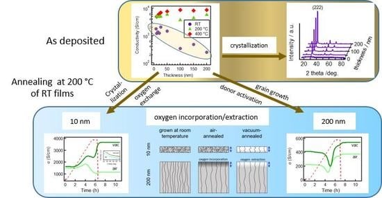
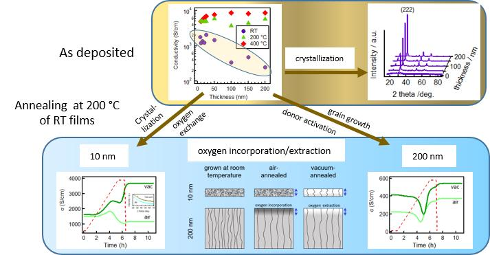
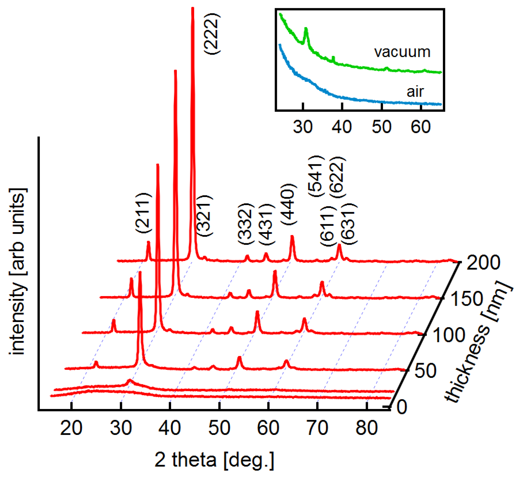
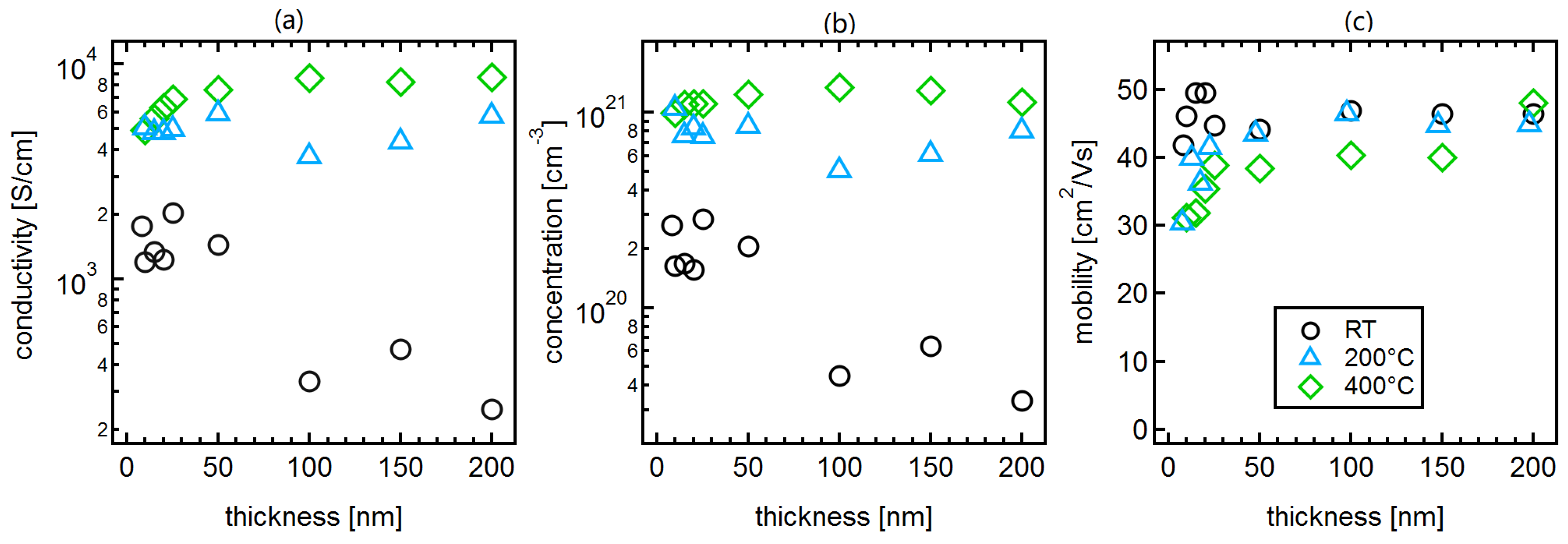
3.1. Influence of Substrate Temperature and Film Thickness
3.1.1. Microstructure of Room Temperature Deposited Films
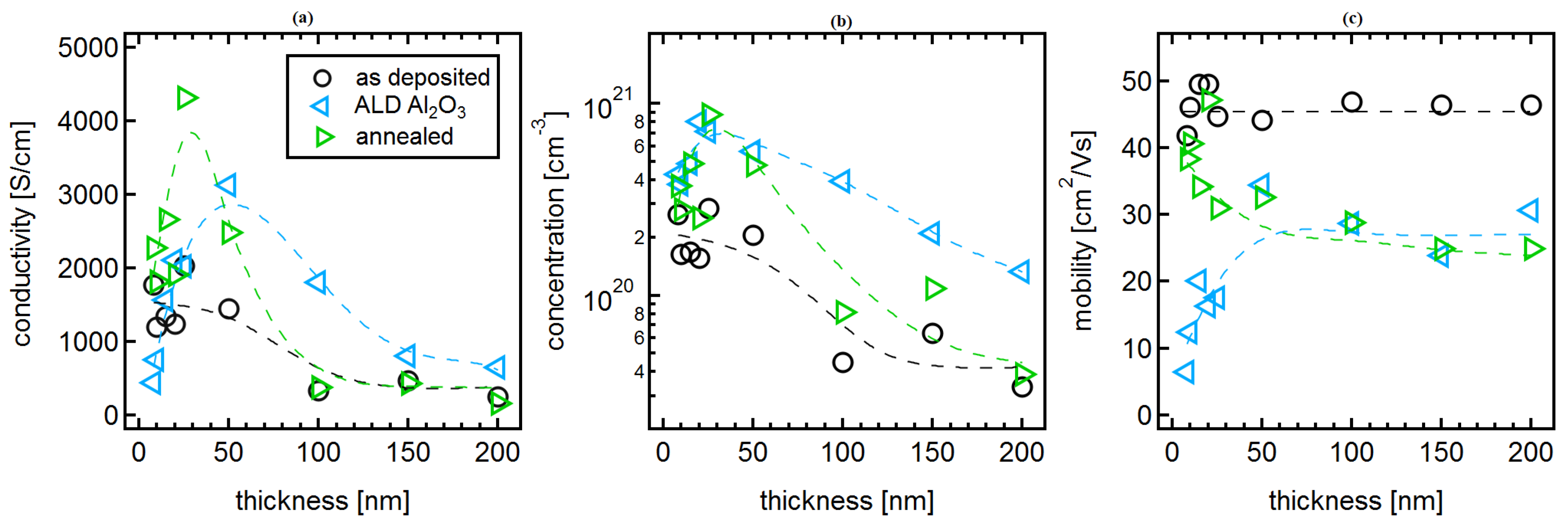
3.1.2. Electrical Properties
3.2. The Effect of Annealing
3.2.1. 200 nm-Thick Films
3.2.2. 10 nm-Thick Films
3.2.3. Extended Annealing in Vacuum
3.3. Effect of AlO Deposition
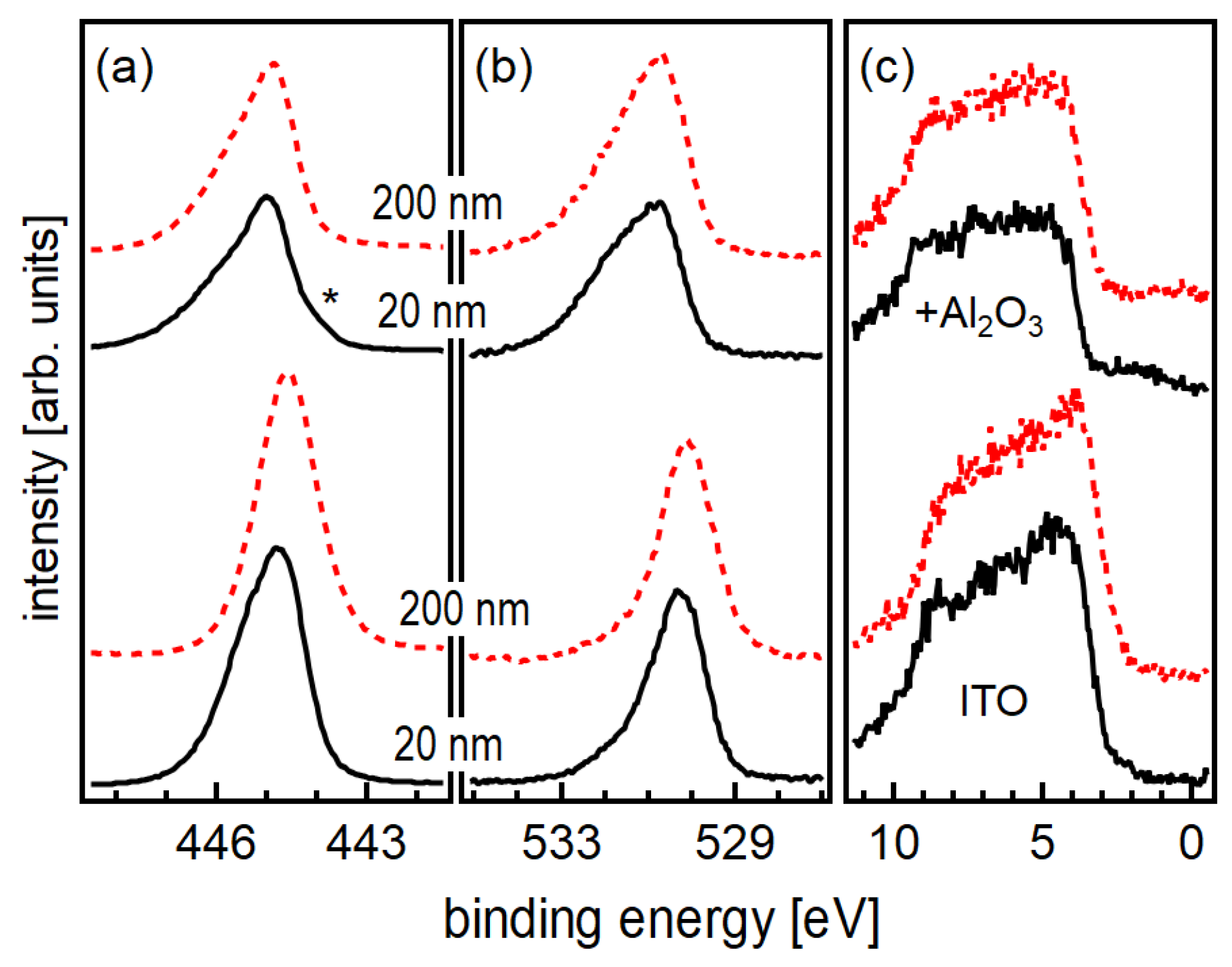
3.3.1. XPS Analysis
3.3.2. Electrical Analysis
4. Summary and Conclusions
Author Contributions
Funding
Acknowledgments
Conflicts of Interest
Abbreviations
| ITO | Sn-doped InO |
| FTO | Fluorine-doped SnO |
| AZO | Al-doped ZnO |
| ALD | atomic-layer-deposition |
| TMA | trimethylaluminium |
| XPS | X-ray photoelectron spectroscopy |
| XRD | X-ray diffraction |
| GIXRD | grazing incidence X-ray diffraction |
| RF | radio frequency |
References
- Ginley, D.S.; Hosono, H.; Paine, D.C. (Eds.) Handbook of Transparent Conductors; Springer: New York, NY, USA, 2010. [Google Scholar]
- Ellmer, K. Past achievements and future challenges in the development of optically transparent electrodes. Nat. Photonics 2012, 6, 809–817. [Google Scholar] [CrossRef]
- Battaglia, C.; Cuevas, A.; Wolf, S.D. High-efficiency crystalline silicon solar cells: Status and perspectives. Energy Environ. Sci. 2016, 9, 1552–1576. [Google Scholar] [CrossRef]
- So, F.; Kido, J.; Burrows, P. Organic Light-Emitting Devices for Solid-State Lighting. MRS Bull. 2008, 33, 663–669. [Google Scholar] [CrossRef]
- Riedl, T.; Gorrn, P.; Kowalsky, W. Transparent Electronics for See-Through AMOLED Displays. J. Disp. Technol. 2009, 5, 501–508. [Google Scholar] [CrossRef]
- Klein, A. Transparent Conducting Oxides: Electronic Structure–Property Relationship from Photoelectron Spectroscopy with in-situ Sample Preparation. J. Am. Ceram. Soc. 2013, 96, 331–345. [Google Scholar] [CrossRef]
- Tahar, R.B.H.; Ban, T.; Ohya, Y.; Takahashi, Y. Tin doped indium oxide thin films: Electrical properties. J. Appl. Phys. 1998, 83, 2631–2645. [Google Scholar] [CrossRef]
- Walukiewicz, W. Intrinsic limitations to the doping of wide-gap semiconductors. Phys. B 2001, 302, 123–134. [Google Scholar] [CrossRef]
- Robertson, J.; Clark, S.J. Limits to doping in oxides. Phys. Rev. B 2011, 83, 075205. [Google Scholar] [CrossRef] [Green Version]
- Lany, S.; Zunger, A. Dopability, Intrinsic Conductivity, and Nonstoichiometry of Transparent Conducting Oxides. Phys. Rev. Lett. 2007, 98, 045501. [Google Scholar] [CrossRef]
- Frank, G.; Köstlin, H. Electrical Properties and Defect Model of Tin-Doped Indium Oxide Layers. Appl. Phys. A 1982, 27, 197–206. [Google Scholar] [CrossRef]
- González, G.B.; Mason, T.O.; Quintana, J.P.; Warschkow, O.; Ellis, D.E.; Hwang, J.H.; Hodges, J.P. Defect structure studies of bulk and nano-indium-tin oxide. J. Appl. Phys. 2004, 96, 3912–3920. [Google Scholar] [CrossRef] [Green Version]
- Yamada, N.; Yasui, I.; Shigesato, Y.; Li, H.; Ujihira, Y.; Nomura, K. Doping Mechanisms of Sn in In2O3 Powder Studied Using 119Sn Mössbauer Spectroscopy and X-Ray Diffraction. Jpn. J. Appl. Phys. 1999, 38, 2856–2862. [Google Scholar] [CrossRef]
- Ágoston, P.; Erhart, P.; Klein, A.; Albe, K. Geometry, electronic structure and thermodynamic stability of intrinsic point defects in indium oxide. J. Phys. Condens. Matter 2009, 21, 455801. [Google Scholar] [CrossRef] [PubMed]
- Ágoston, P.; Körber, C.; Klein, A.; Puska, M.J.; Nieminen, R.M.; Albe, K. Limits for n-type doping in In2O3 and SnO2: A theoretical approach by first-principles calculations using hybrid-functional methodology. J. Appl. Phys. 2010, 108, 053511. [Google Scholar] [CrossRef]
- Gassenbauer, Y.; Schafranek, R.; Klein, A.; Zafeiratos, S.; Hävecker, M.; Knop-Gericke, A.; Schlögl, R. Surface states, surface potentials and segregation at surfaces of tin-doped In2O3. Phys. Rev. B 2006, 73, 245312. [Google Scholar] [CrossRef]
- Ágoston, P.; Albe, K. Ab initio modeling of diffusion in indium oxide. Phys. Rev. B 2010, 81, 195205. [Google Scholar] [CrossRef]
- Hohmann, M.V.; Wachau, A.; Klein, A. In situ Hall effect and conductivity measurements of ITO thin films. Solid State Ion. 2014, 262, 636–639. [Google Scholar] [CrossRef]
- Frischbier, M.V.; Wardenga, H.F.; Weidner, M.; Bierwagen, O.; Jia, J.; Shigesato, Y.; Klein, A. Influence of dopant species and concentration on grain boundary scattering in degenerately doped In2O3 thin films. Thin Solid Films 2016, 614, 62–68. [Google Scholar] [CrossRef]
- Song, P.K.; Akao, H.; Kamei, M.; Shigesato, Y.; Yasui, I. Preparation and Crystallization of Tin-doped and Undoped Amorphous Indium Oxide Films Deposited by Sputtering. Jpn. J. Appl. Phys. 1999, 38, 5224. [Google Scholar] [CrossRef]
- Nunes de Carvalho, C.; Luis, A.; Lavareda, G.; Fortunato, E.; Amaral, A. Effect of thickness on the properties of ITO thin films deposited by RF-PERTE on unheated, flexible, transparent substrates. Surf. Coat. Technol. 2002, 151, 252–256. [Google Scholar] [CrossRef]
- Kim, D.; Han, Y.; Cho, J.S.; Koh, S.K. Low temperature-deposition of ITO thin films by ion beam sputtering. Thin Solid Films 2000, 377, 81–86. [Google Scholar] [CrossRef]
- Hao, L.; Diao, X.; Xu, H.; Gu, B.; Wang, T. Thickness dependence of structural, electrical and optical properties of indium tin oxide (ITO) films deposited on PET substrates. Appl. Surf. Sci. 2008, 254, 3504–3508. [Google Scholar] [CrossRef]
- Kim, S.T.; Kim, T.G.; Cho, H.; Yoon, S.J.; Kim, H.S.; Kim, J.K. Thickness Dependence of Properties of ITO Films Deposited on PET Substrates. J. Nanosci. Nanotechnol. 2016, 16, 1852–1854. [Google Scholar] [CrossRef]
- Bellingham, J.R.; Phillips, W.A.; Adkins, C.J. Electrical and optical properties of amorphous indium oxide. J. Phys. Condens. Matter 1990, 2, 6207–6221. [Google Scholar] [CrossRef]
- Medvedeva, J.E.; Buchholz, D.B.; Chang, R.P.H. Recent advances in understanding the structure and properties of amorphous oxide semiconductors. Adv. Electr. Mater. 2017, 3, 1700082. [Google Scholar] [CrossRef]
- Lohaus, C.; Steinert, C.; Deyu, G.; Brötz, J.; Jaegermann, W.; Klein, A. Enhancing electrical conductivity of room-temperature-deposited Sn-doped In2O3 thin films by hematite seed layers. Appl. Phys. Lett. 2018, 112, 152105. [Google Scholar] [CrossRef]
- Koida, T.; Ueno, Y.; Shibata, H. In2O3-Based Transparent Conducting Oxide Films with High Electron Mobility Fabricated at Low Process Temperatures. Phys. Stat. Sol. A 2018, 215, 1700506. [Google Scholar] [CrossRef]
- Koida, T.; Fujiwara, H.; Kondo, M. Hydrogen-doped In2O33 as high-mobility transparent conductive oxide. Jpn. J. Appl. Phys. 2007, 46, L685–L687. [Google Scholar] [CrossRef]
- Koida, T.; Kondo, M.; Tsutsumi, K.; Sakaguchi, A.; Suzuki, M.; Fujiwara, H. Hydrogen-doped In2O3 transparent conducting oxide films prepared by solid-phase crystallization method. J. Appl. Phys. 2010, 107, 033514. [Google Scholar] [CrossRef]
- Weidner, M.; Fuchs, A.; Bayer, T.J.M.; Rachut, K.; Schnell, P.; Deyu, G.K.; Klein, A. Defect Modulation Doping. Adv. Funct. Mater. 2019, 29, 1807906. [Google Scholar] [CrossRef]
- Bayer, T.J.M.; Wachau, A.; Fuchs, A.; Deuermeier, J.; Klein, A. Atomic layer deposition of Al2O3 onto Sn-doped In2O3: Absence of self-limited adsorption during initial growth by oxygen diffusion from the substrate and band offset modification by Fermi level pinning in Al2O3. Chem. Mater. 2012, 24, 4503–4510. [Google Scholar] [CrossRef]
- Wardenga, H.; Frischbier, M.V.; Morales-Masis, M.; Klein, A. In-situ Hall-effect monitoring of vacuum annealing of In2O3:H thin films. Materials 2015, 91, 561–574. [Google Scholar] [CrossRef] [PubMed]
- Khanal, R.; Buchholz, D.B.; Chang, R.P.H.; Medvedeva, J.E. Composition-dependent structural and transport properties of amorphous transparent conducting oxides. Phys. Rev. B 2015, 91, 205203. [Google Scholar] [CrossRef] [Green Version]
- Park, J.O.; Lee, J.H.; Kim, J.J.; Cho, S.H.; Cho, Y.K. Crystallization of indium tin oxide thin films prepared by RF-magnetron sputtering without external heating. Thin Solid Films 2005, 474, 127–132. [Google Scholar] [CrossRef]
- Mattox, D.M. Particle bombardment effects on thin-film deposition: A review. J. Vac. Sci. Technol. A 1989, 7, 1105–1114. [Google Scholar] [CrossRef]
- Seto, J.Y.W. The electrical properties of polycrystalline silicon films. J. Appl. Phys. 1975, 46, 5247–5254. [Google Scholar] [CrossRef]
- Ellmer, K. Electrical Properties. In Transparent Conductive Zinc Oxide; Ellmer, K., Klein, A., Rech, B., Eds.; Springer: Berlin, Germany, 2008; pp. 35–78. [Google Scholar]
- Sommer, N.; Hüpkes, J.; Rau, U. Field Emission at Grain Boundaries: Modeling the Conductivity in Highly Doped Polycrystalline Semiconductors. Phys. Rev. Appl. 2016, 5, 024009. [Google Scholar] [CrossRef] [Green Version]
- Preissler, N.; Bierwagen, O.; Ramu, A.T.; Speck, J.S. Electrical transport, electrothermal transport, and effective electron mass in single-crystalline In2O3 films. Phys. Rev. B 2013, 88, 085305. [Google Scholar] [CrossRef]
- Sze, S.M.; Ng, K.K. Physics of Semiconductor Devices; John Wiley & Sons: Hoboken, NJ, USA, 2007. [Google Scholar]
- Maier, J. Physical Chemistry of Ionic Materials; Wiley-VCH: Weinheim, Germany, 2004. [Google Scholar]
- Merkle, R.; Maier, J. How Is Oxygen Incorporated into Oxides? A Comprehensive Kinetic Study of a Simple Solid-State Reaction with SrTiO3 as a Model Material. Angew. Chem. Int. Ed. 2008, 47, 3874–3894. [Google Scholar] [CrossRef]
- Crank, J. The Mathematics of Diffusion; Oxford University Press: Oxford, UK, 1975. [Google Scholar]
- Sytchkova, A.; Zola, D.; Bailey, L.R.; Mackenzie, B.; Proudfoot, G.; Tian, M.; Ulyashin, A. Depth dependent properties of ITO thin films grown by pulsed DC sputtering. Mater. Sci. Eng. B 2013, 178, 586–592. [Google Scholar] [CrossRef] [Green Version]
- King, P.D.C.; Veal, T.D.; Payne, D.J.; Bourlange, A.; Egdell, R.G.; McConville, C.F. Surface Electron Accumulation and the Charge Neutrality Level in In2O3. Phys. Rev. Lett. 2008, 101, 116808. [Google Scholar] [CrossRef] [PubMed]
- King, P.D.C.; Veal, T.D.; Fuchs, F.; Wang, C.Y.; Payne, D.J.; Bourlange, A.; Zhang, H.; Bell, G.R.; Cimalla, V.; Ambacher, O.; et al. Band gap, electronic structure, and surface electron accumulation of cubic and rhombohedral In2O3. Phys. Rev. B 2009, 79, 205211. [Google Scholar] [CrossRef]
- Bierwagen, O. Indium oxide—A transparent, wide-band gap semiconductor for (opto)electronic applications. Semicond. Sci. Technol. 2015, 30, 024001. [Google Scholar] [CrossRef]
- Berthold, T.; Rombach, J.; Stauden, T.; Polyakov, V.; Cimalla, V.; Krischok, S.; Bierwagen, O.; Himmerlich, M. Consequences of plasma oxidation and vacuum annealing on the chemical properties and electron accumulation of In2O3 surfaces. J. Appl. Phys. 2016, 120, 245301. [Google Scholar] [CrossRef]
- Hillmann, S.; Rachut, K.; Bayer, T.J.M.; Li, S.; Klein, A. Application of atomic layer deposited Al2O3 as charge injection layer for high-permittivity dielectrics. Semicond. Sci. Technol. 2015, 30, 024012. [Google Scholar] [CrossRef]
- Deuermeier, J.; Bayer, T.; Yanagi, H.; Kiazadeh, A.; Martins, R.; Klein, A.; Fortunato, E. Substrate reactivity as origin of Fermi level pinning at the Cu2O/ALD-Al2O3 interface. Mater. Res. Expr. 2016, 3, 046404. [Google Scholar] [CrossRef]
- Li, S.; Chen, F.; Schafranek, R.; Bayer, T.J.M.; Rachut, K.; Fuchs, A.; Siol, S.; Weidner, M.; Hohmann, M.; Pfeifer, V.; et al. Intrinsic energy band alignment of functional oxides. Phys. Stat. Sol. (RRL) 2014, 8, 571–576. [Google Scholar] [CrossRef]
- Siol, S.; Hellmann, J.C.; Tilley, S.D.; Graetzel, M.; Morasch, J.; Deuermeier, J.; Jaegermann, W.; Klein, A. Band Alignment Engineering at Cu2O/ZnO Heterointerfaces. Acs Appl. Mater. Interfaces 2016, 8, 21824–21831. [Google Scholar] [CrossRef]
- Giesecke, R.; Hertwig, R.; Bayer, T.; Randall, C.A.; Klein, A. Modification of the Cathodic Schottky Barrier Height at the RuO2 Cathode During Resistance Degradation of Fe-doped SrTiO3. J. Am. Ceram. Soc. 2017, 100, 4590–4601. [Google Scholar] [CrossRef]
- Gregori, G.; Merkle, R.; Maier, J. Ion conduction and redistribution at grain boundaries in oxide systems. Prog. Mater. Sci. 2017, 89, 252–305. [Google Scholar] [CrossRef]
- Groner, M.D.; Fabreguette, F.H.; Elam, J.W.; George, S.M. Low-Temperature Al2O3 Atomic Layer Deposition. Chem. Mater. 2004, 16, 639–645. [Google Scholar] [CrossRef]
- Kot, M.; Das, C.; Wang, Z.; Henkel, K.; Rouissi, Z.; Wojciechowski, K.; Snaith, H.J.; Schmeisser, D. Room-Temperature Atomic Layer Deposition of Al2O3: Impact on Efficiency, Stability and Surface Properties in Perovskite Solar Cells. ChemSusChem 2016, 9, 3401–3406. [Google Scholar] [CrossRef] [PubMed]


© 2019 by the authors. Licensee MDPI, Basel, Switzerland. This article is an open access article distributed under the terms and conditions of the Creative Commons Attribution (CC BY) license (http://creativecommons.org/licenses/by/4.0/).
Share and Cite
Deyu, G.K.; Hunka, J.; Roussel, H.; Brötz, J.; Bellet, D.; Klein, A. Electrical Properties of Low-Temperature Processed Sn-Doped In2O3 Thin Films: The Role of Microstructure and Oxygen Content and the Potential of Defect Modulation Doping. Materials 2019, 12, 2232. https://doi.org/10.3390/ma12142232
Deyu GK, Hunka J, Roussel H, Brötz J, Bellet D, Klein A. Electrical Properties of Low-Temperature Processed Sn-Doped In2O3 Thin Films: The Role of Microstructure and Oxygen Content and the Potential of Defect Modulation Doping. Materials. 2019; 12(14):2232. https://doi.org/10.3390/ma12142232
Chicago/Turabian StyleDeyu, Getnet Kacha, Jonas Hunka, Hervé Roussel, Joachim Brötz, Daniel Bellet, and Andreas Klein. 2019. "Electrical Properties of Low-Temperature Processed Sn-Doped In2O3 Thin Films: The Role of Microstructure and Oxygen Content and the Potential of Defect Modulation Doping" Materials 12, no. 14: 2232. https://doi.org/10.3390/ma12142232