
Buck Converter with Soft-Switching Cells for PV Panel Applications

Department of Electrical Engineering, National Chin-Yi University of Technology, Taichung 41170, Taiwan
*
Author to whom correspondence should be addressed.
Energies 2016, 9(3), 148; https://doi.org/10.3390/en9030148
Submission received: 24 November 2015
/
Revised: 15 February 2016
/
Accepted: 25 February 2016
/
Published: 2 March 2016
Abstract
:In power conversion of photovoltaic (PV) energy, a hard-switching buck converter always generates some disadvantages. For example, serious electromagnetic interference (EMI), high switching losses, and stresses on an active switch (metal-oxide-semiconductor-field-effect-transistor, MOSFET), and high reverse-recovery losses of a freewheeling diode result in low conversion efficiency. To release these disadvantages, a buck converter with soft-switching cells for PV panel applications is proposed. To create zero-voltage-switching (ZVS) features of the active switches, a simple active soft-switching cell with an inductor, a capacitor, and a MOSFET is incorporated into the proposed buck converter. Therefore, the switching losses and stresses of the active switches and EMI can be reduced significantly. To reduce reverse-recovery losses of a freewheeling diode, a simple passive soft-switching cell with a capacitor and two diodes is implemented. To verify the performance and the feasibility of the proposed buck converter with soft-switching cells for PV panel applications, a prototype soft-switching buck converter is built and implemented by using a maximum-power-point-tracking (MPPT) method. Simulated and experimental results are presented from a 100 W soft-switching buck converter for PV panel applications.
1. Introduction
Due to the fact that human beings overuse fossil fuels, environmental pollution and greenhouse effects of the earth occur [1].The development of renewable energies and reduction of greenhouse effects has been an important topic. Among all the renewable energies, solar energy attracts more interests owing to its noiseless, pollution-free, non-radioactive, and inexhaustible characteristics. Currently, solar energy is converted into electric power through PV panels. Due to having a very long lifetime and being a very flexible kind of energy source, PV panels have popularly applied to power system. However, with the instable and intermittent characteristics, PV panels cannot provide stable power output. Thus, PV panels often need to incorporate a MPPT algorithm and a switching power converter for providing high-quality dc power to the load [2,3,4]. Higher performance, smaller volume, and lighter weight have spurred the research of switching power converters to design converters operated at high frequency. The objective of high frequency operation in switching power converters is to reduce the size and cost of passive components.
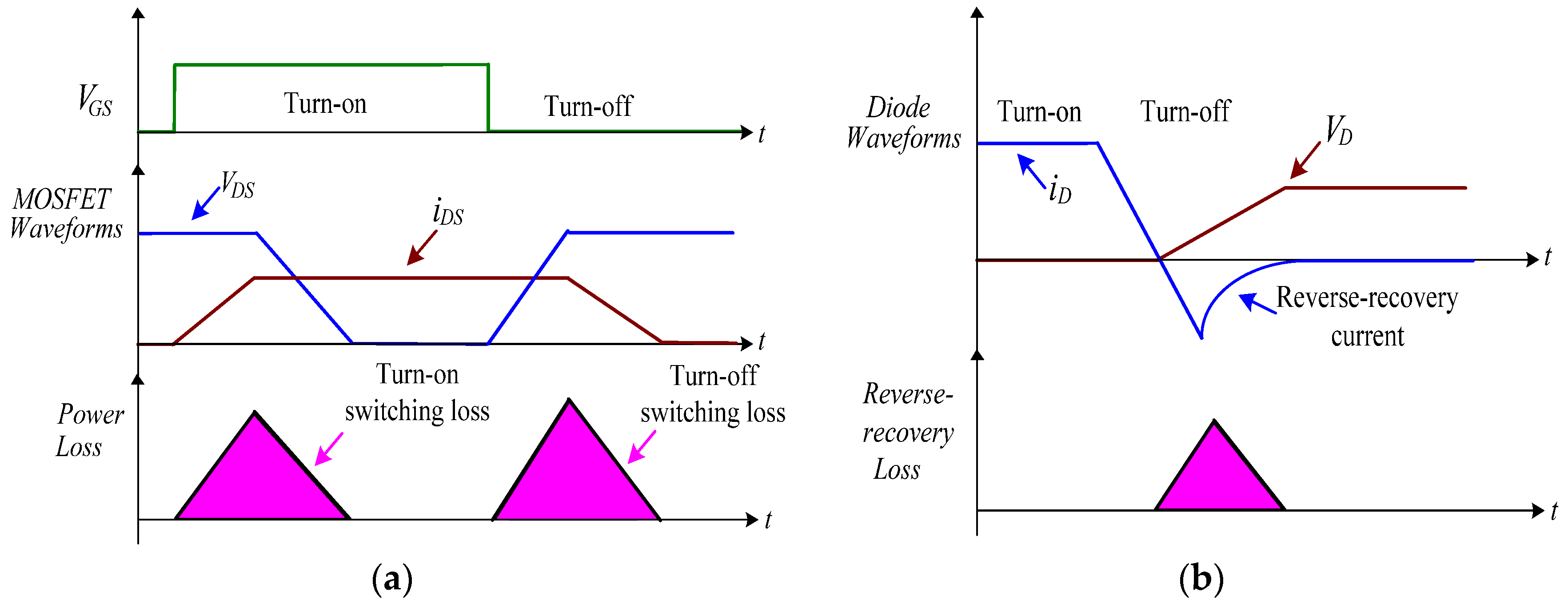
A number of non-isolated switching power converters have been developed and proposed [5]. For example: buck, boost, Ćuk, zeta, and sepic converters are attracted, which have simple constructions and are widely used in low and medium power. To step-down voltage and non-isolated applications, the buck converter is often adopted. However, the hard-switching condition of the active switch (MOSFET) and the reverse-recovery current of the freewheeling diode are major contributors to switching losses in the buck converter, resulting in high power losses, high EMI, and low conversion efficiency. The illustrations of the hard-switching for the active switch and the freewheeling diode are shown in Figure 1. As the switching frequency increases, the power losses and EMI in the buck converter increase. To overcome these problems, a relatively large number of soft-switching techniques have been proposed [6,7]. The soft-switching techniques improve the imperfect switching of the power switches and thereby eliminate switching losses and EMI.
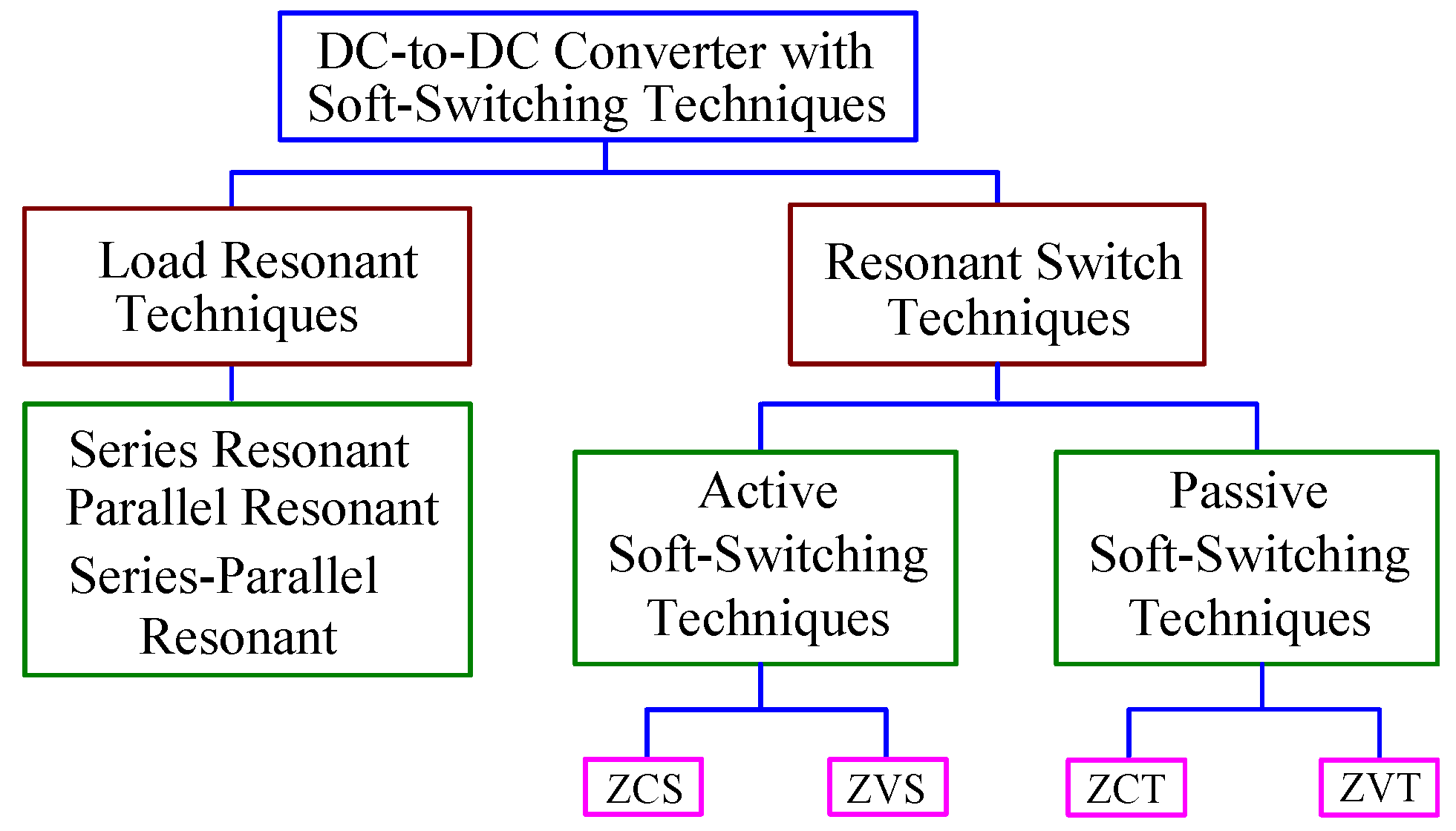
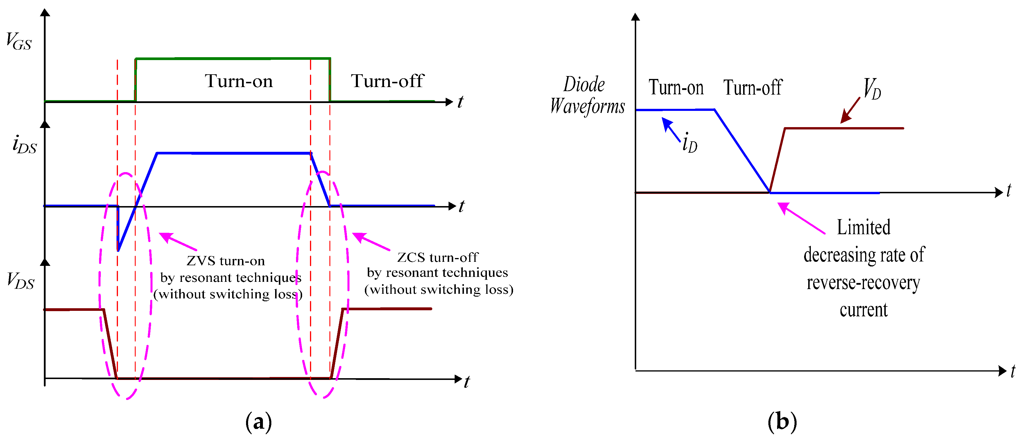
Several soft-switching techniques were developed in recent years. Figure 2 shows a classification of DC-to-DC converters with soft-switching techniques. In general, the load resonant techniques require a relatively large resonant inductor, which creates a large amount of circulation energy, resulting in more conduction loss, and their current or voltage stresses are higher than that of the resonant switch techniques. Resonant switch techniques can be categorized into active soft-switching techniques and passive soft-switching techniques. The active soft-switching techniques can be divided into ZVS and zero-current-switching (ZCS) techniques [8,9]. The ZVS or ZCS technique drives the voltage or current of the active switch to zero before any switching action, and avoids the concurrent high voltage and high current in the switching transition, as shown in Figure 3a. The passive soft-switching techniques can be divided into zero-voltage-transition (ZVT) and zero-current-transition (ZCT) techniques. The passive soft-switching techniques can limit the decreasing rate of reverse-recovery currents of the freewheeling diode, and avoid the reverse-recovery losses in the switching transition, as shown in Figure 3b. However, the auxiliary switches of the passive soft-switching techniques are still turned off in hard switching and the losses at the auxiliary switches might be significant, especially in high frequency applications. Comparing the active and passive soft-switching techniques, the active soft-switching techniques are an effective means to solve or alleviate switching losses, stresses, and EMI problems [10].
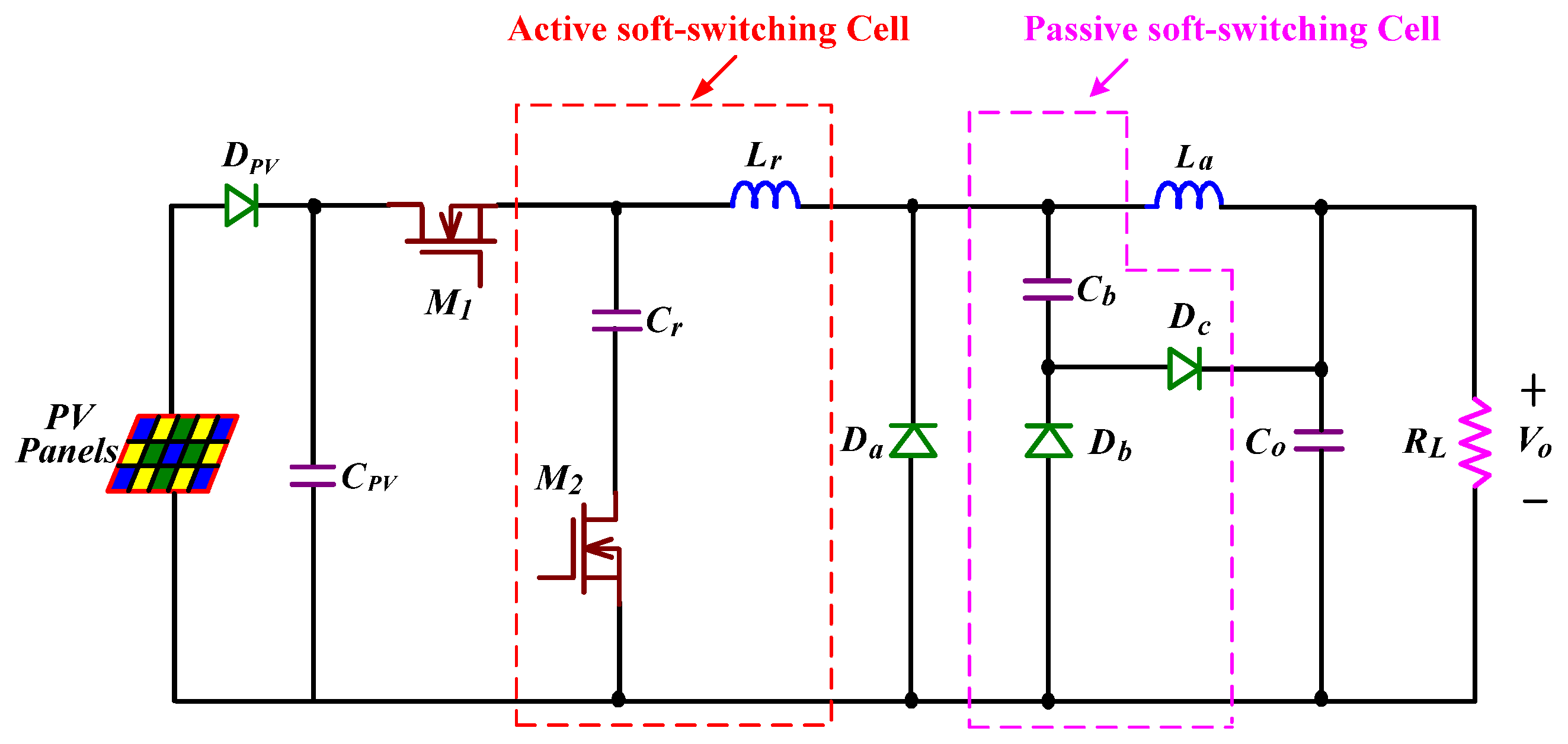
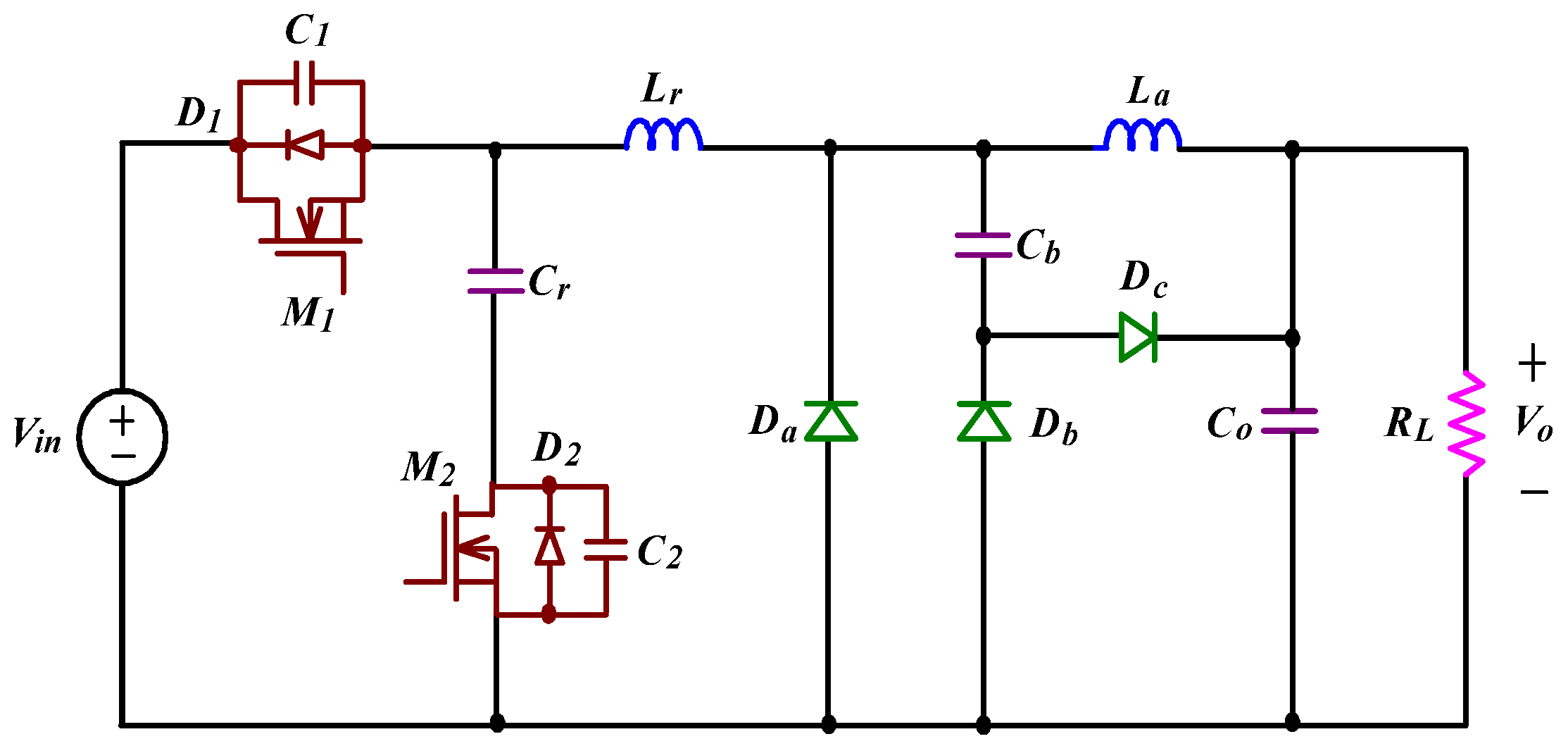
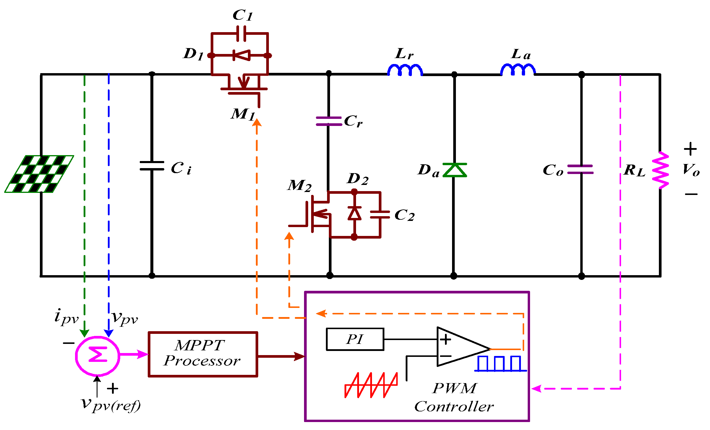
In this paper, a buck converter with soft-switching cells for PV panel applications is presented, as shown in Figure 4. The proposed buck converter incorporates an active soft-switching cell and a passive soft-switching cell. The active soft-switching cell is a simple structure, which consists of a resonant inductor (Lr), a resonant capacitor (Cr), and an auxiliary switch (M2) to implement the ZVS features of the main switch (M1) and auxiliary switch (M2). Furthermore, the passive soft-switching cell is also a simple structure, which consists of a buffer capacitor (Cb) and two diodes (Db and Dc) to limit the decreasing rate of reverse-recovery currents of the freewheeling diode (Da). The operational principles of the proposed soft-switching buck converter are described in Section 2. In order to achieve the fast dynamic response and high conversion efficiency of the proposed soft-switching buck converter, the design considerations of the soft-switching cells and the MPPT method are described in Section 3. Experimental results obtained from a prototype with the proposed soft-switching buck converter for PV panel applications are presented in Section 4. Finally, a conclusion is given in Section 5.
2. Operational Principles
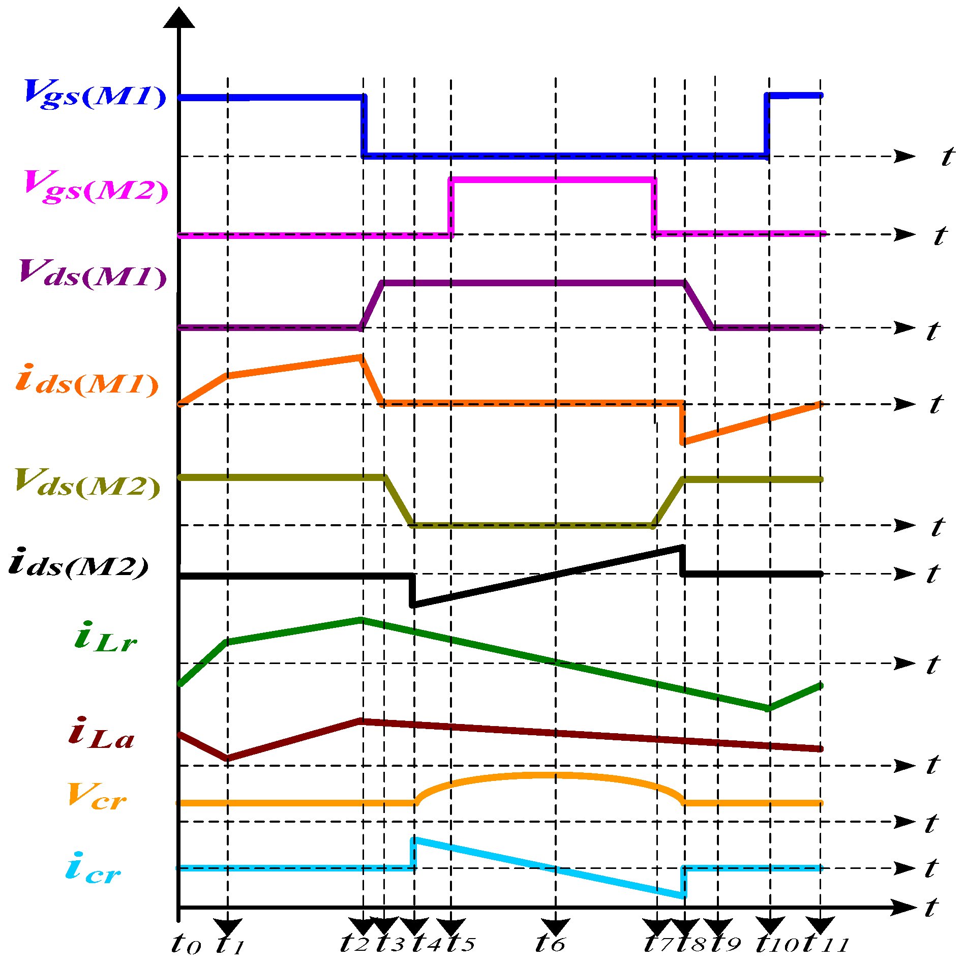
Figure 4 shows the circuit structure of the proposed buck converter with soft-switching cells for PV panel applications. For convenience of illustration and analysis, the PV panels of Figure 4 can be seen as a source of constant voltage. It is simplified and redrawn in Figure 5. To facilitate the operational principles, Figure 6 shows conceptual current and voltage waveforms of the key components and the driving signal switches (M1 and M2). Figure 7 shows the topological modes of the proposed soft-switching buck converter during a switching cycle. To simplify the description of the operational modes, the following assumptions are made:
- (1)
- To analyze the ZVS features, the body diodes (D1 and D2) and parasitic capacitors (C1 and C2) of the main and auxiliary switches (M1 and M2) will be considered at the steady-state operation of the circuit.
- (2)
- All of the components are ideal.
The operational modes of the proposed soft-switching buck converter can be divided into 11 modes and explained mode by mode as follows:
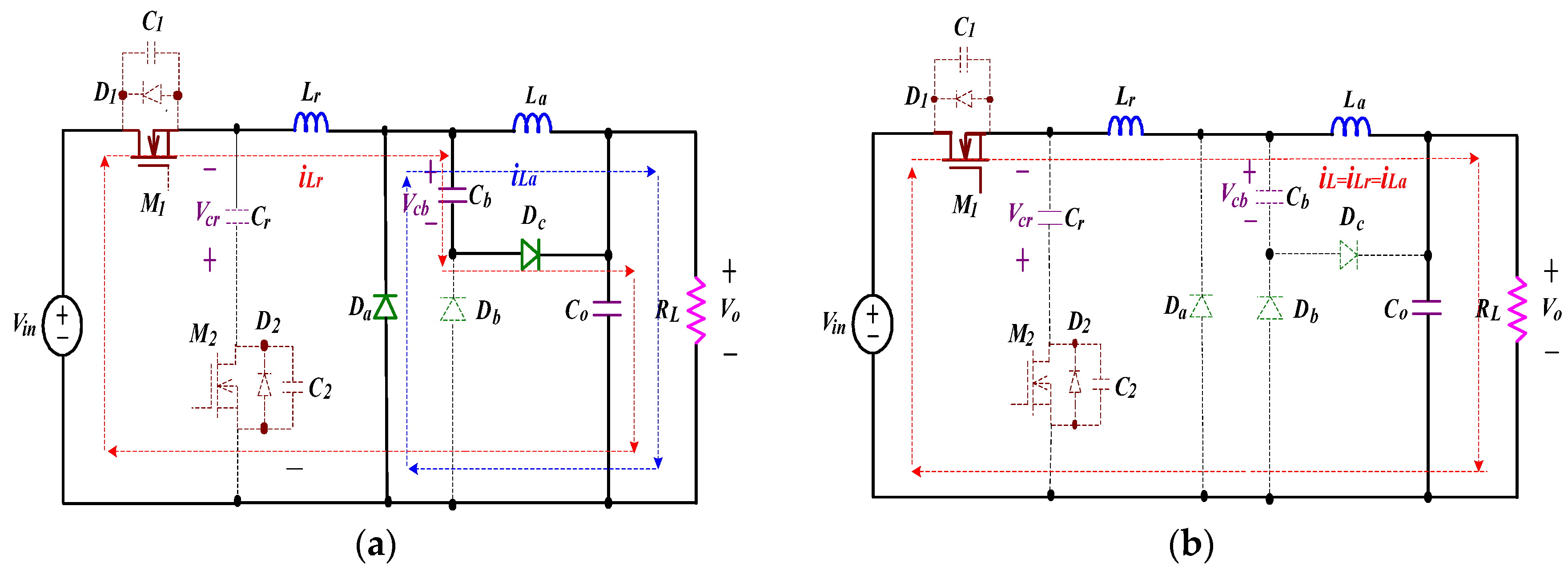
At time t0, the main switch (M1) is turned on and the auxiliary switch (M2) is turned off, continually. The current iLr of resonant inductor flowing through the resonant inductor (Lr), the buffer capacitor (Cb), diode (Dc) and load (RL) is linearly increased. During this interval, the current iLa of the storage inductor flowing through the load freewheeling diode (Da) is linearly decreased. The current iLr of the resonant inductor and the current iLa of the storage inductor can be expressed as:
and
The equivalent circuit of mode 1 is shown in Figure 7a.
At time t1, the current iLr of the resonant inductor equals the current iLa of the stored inductor, and the voltage of the buffer capacitor (Cb) is charged to VLa + Vo. Thus, the freewheeling diode (Da) is turned off. The current iL can be expressed as:
where iL = iLr = iLa. The equivalent circuit of mode 2 is shown in Figure 7b.
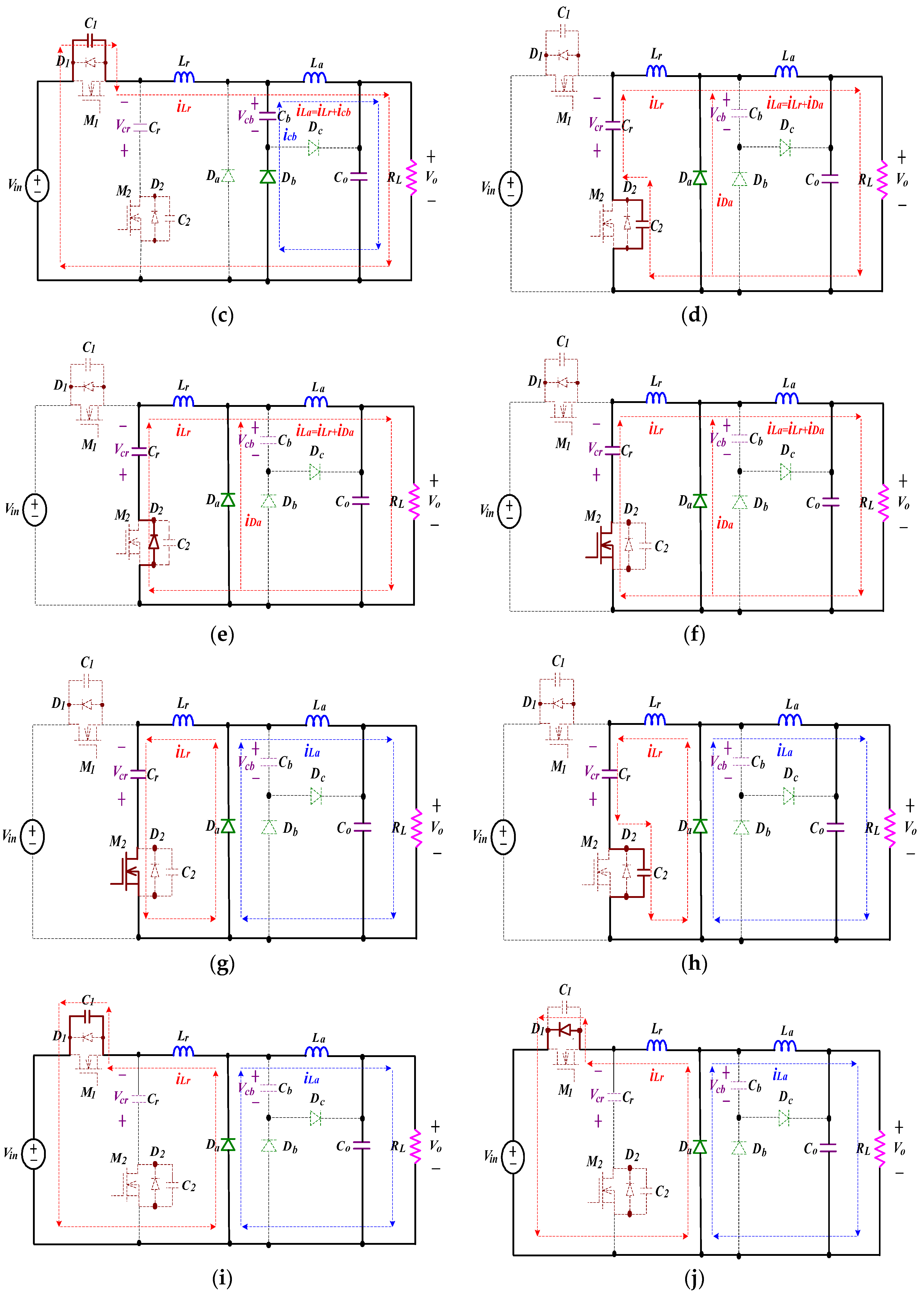
At time t2, the main switch (M1) is turned off and the auxiliary switch (M2) is maintained off. During this interval, the parasitic capacitor (C1) of the main switch (M1) is charged and the current iL is continuously increased. Simultaneously, the buffer capacitor (Cb) begins discharging by the stored inductor (La), load (RL), and diode (Db). The stored inductor current iLa can be expressed as:
The equivalent circuit of mode 3 is shown in Figure 7c.
At time t3, the drain-source voltage (VDS1) of the main switch (M1) is charged to Vin−(VLr + VLa + Vo), and the voltage of the buffer capacitor (Cb) is dropped to zero. Thus, the freewheeling diode (Da) is turned on. The current iLa is divided into two branches: one is the current iLr of the resonant inductor (Lr), and another is the current iDa of the freewheeling diode (Da).The resonant inductor (Lr)releases its energy to the parasitic capacitance(C2) of the auxiliary switch (M2). To achieve a ZVS feature for auxiliary switch (M2), the energy stored in resonant inductor (Lr) should satisfy the following inequality:
The stored inductor current iLa can be expressed as:
The equivalent circuit of mode 4 is shown in Figure 7d.
At time t4, the voltage (VDS2) of the auxiliary switch (M2) is discharged down to zero. The current iLr of the resonant inductor forces the body diode (D2) of the auxiliary switch (M2) conducting, and a ZVS feature will be created for the auxiliary switch (M2). The current iLr of the resonant inductor and the current iLa of the stored inductor can be expressed as:
and
The equivalent circuit of mode 5 is shown in Figure 7e.
At time t5, the auxiliary switch (M2) is turned on under ZVS condiction. In this operational mode, the resonant inductor (Lr) begins resonant with the resonant capacitor (Cr), while the energy trapped in the resonant inductor (Lr) is recycled to resonant capacitor (Cr).The current iLr of the resonant inductor, the voltage (VLr) of the resonant inductor and the voltage (VCr) of the resonant capacitor can be expressed as follows:
and
where characteristic impedance is and resonant frequency is . The equivalent circuit of mode 6 is shown in Figure 7f.
At time t6, the energy of the resonant inductor (Lr) is released to zero. Then, the iLr of the resonant inductor current reverses its direction and the resonant capacitor (Cr) begins to release its stored energy through (M2) and (Lr). The current iLr of the resonant inductor and the current iLa of the stored inductor can be expressed as:
and
The equivalent circuit of mode 7 is shown in Figure 7g.
At time t7, the auxiliary switch (M2) is turned off, and the parasitic capacitance (C2) of the auxiliary switch (M2) is charged. The resonant capacitor (Cr) continuously releases its stored energy through (M2) and (Lr). The current iLr of the resonant inductor and the current iLa of the stored inductor can be expressed as:
and
The equivalent circuit of mode 8 is shown in Figure 7h.
At time t8, when the voltage (VDS2) of the auxiliary switch (M2) is equal to Vin + VDS1 + VCr, the current iLr of the resonant inductor will flow through the parasitic capacitance (C1) of the main switch (M1). At this interval, the energies stored in the parasitic capacitance (C1) of the main switch (M1) begin discharging. To achieve a ZVS feature for main switch (M1), the energy stored in the resonant inductor (Lr) should satisfy the following inequality:
The current iLa of the stored inductor can be expressed as:
The equivalent circuit of mode 9 is shown in Figure 7i.
At time t9, the energies stored in the parasitic capacitance (C1) of the main switch (M1) are discharged down to zero. The current iLr of the resonant inductor forces the body diode (D1) of the main switch (M1) conducting, and a ZVS feature will be created for the main switch (M1). The current iLr of the resonant inductor and the current iLa of the stored inductor can be expressed as:
and
The equivalent circuit of mode 10 is shown in Figure 7j.
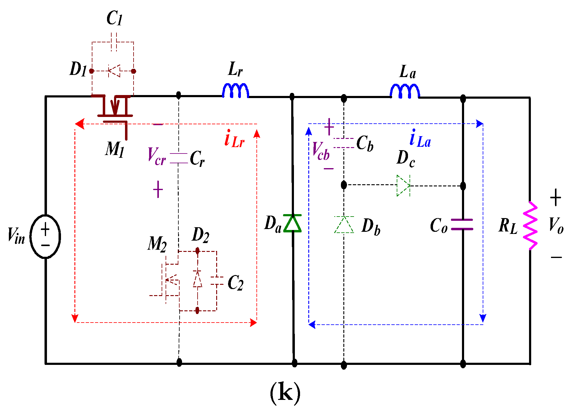
At time t10, the main switch (M1) is turned on under ZVS condiction. When the current iLr of the resonant inductor is discharged to zero at time t11, it will be forwarded and flow through the resonant inductor (Lr), the buffer capacitor (Cb), diode (Dc), and load (RL). The equivalent circuit of mode 11 is shown in Figure 6k.The operation of the proposed soft-switching buck converter over one switching cycle is completed.
3. Selections of Soft-Switching Cells and MPPT
In order to achieve the fast dynamic response and high conversion efficiency, an optimal control scheme must be integrated into the proposed soft-switching buck converter for PV panel applications. The optimal control scheme includes the selection of the MPPT method and the soft-switching cells. In this section, the selections of the design methods will be described in detail as follows.
3.1. Selection of Soft-Switching Cells
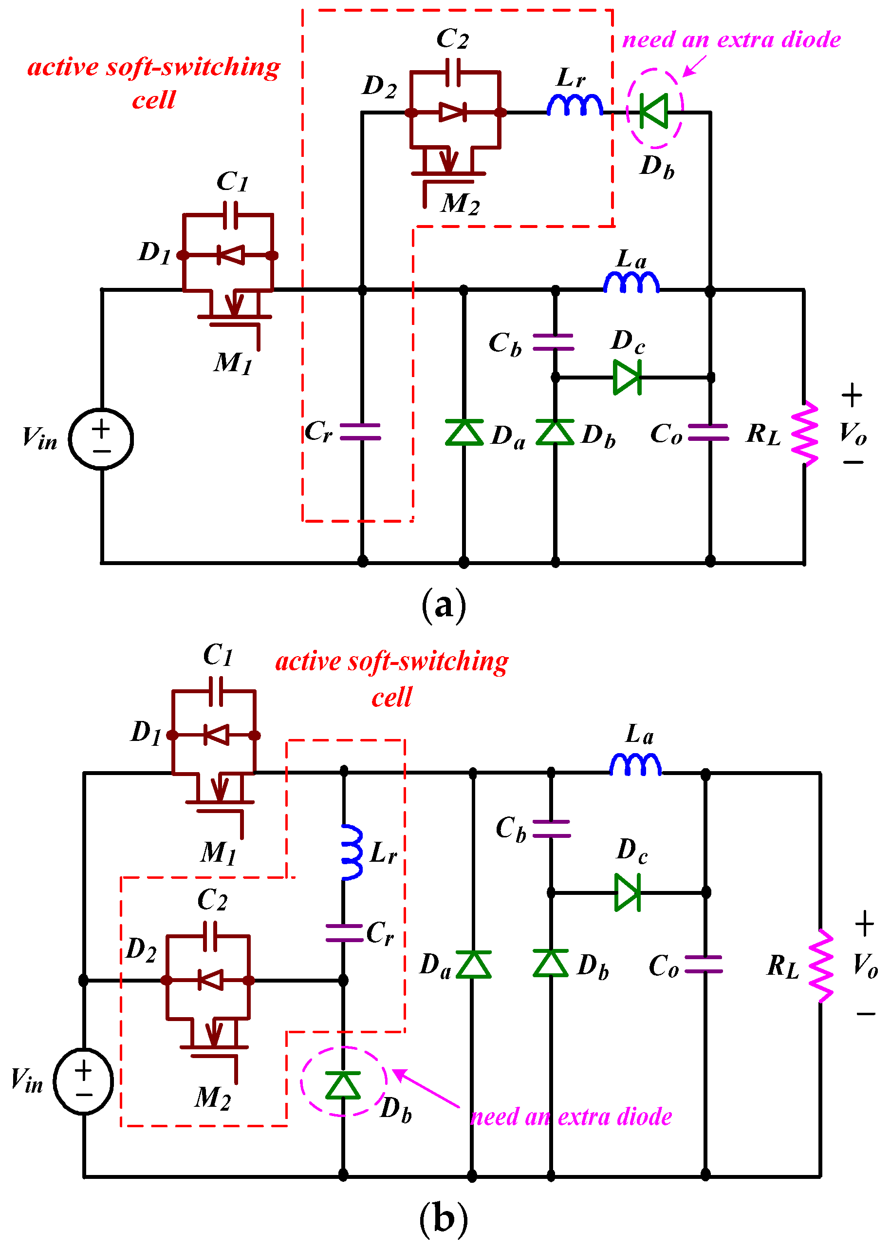
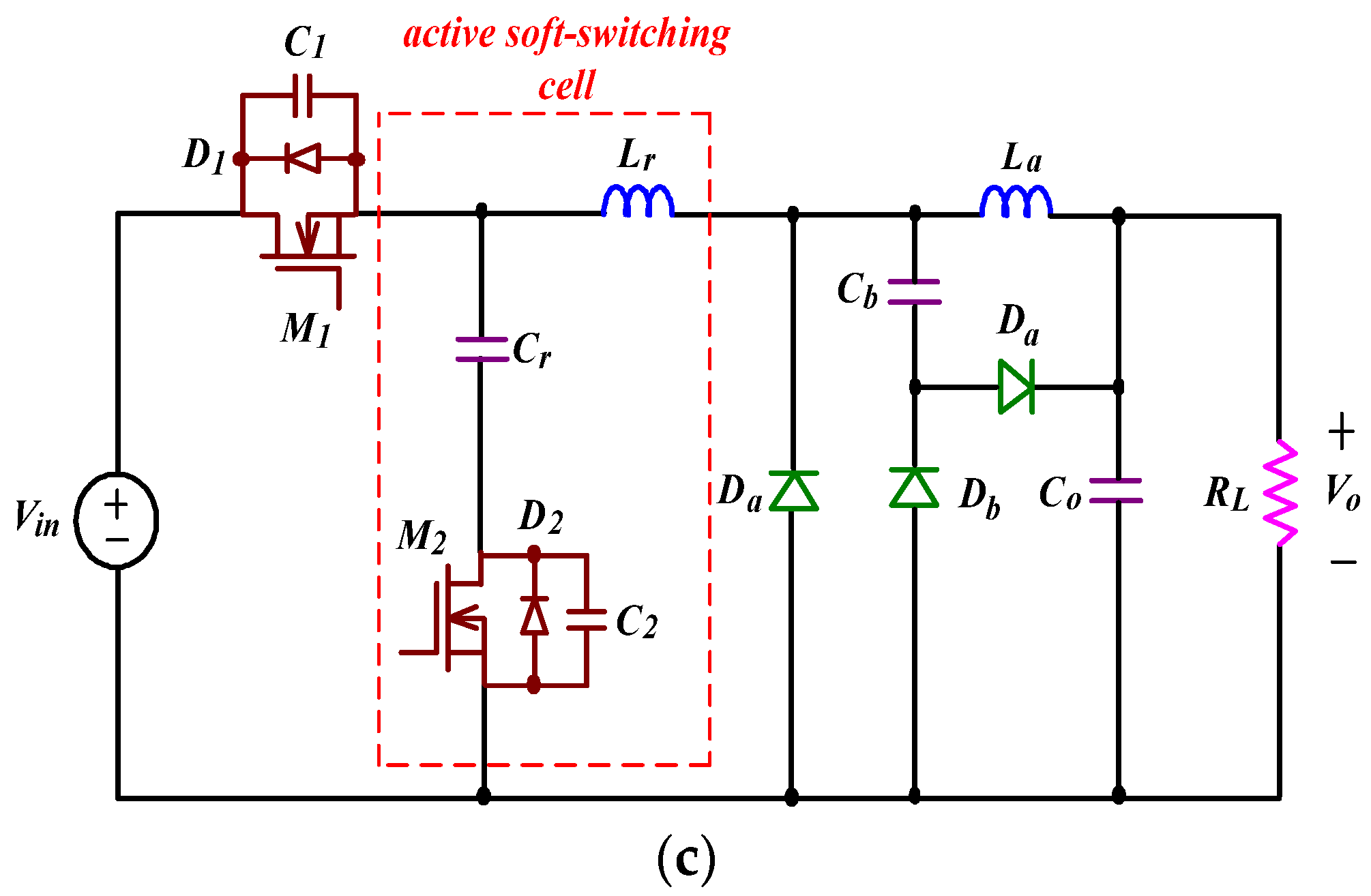
To reduce switching losses and increase conversion efficiency, a buck converter with soft-switching cells to implement ZVS features of active switches is usually adopted. The composition of the active soft-switching cell needs at least three main components, including an active switch, a resonant inductor, and a resonant capacitor [11,12]. The possible combinations of an active soft-switching cell in a typical buck converter are shown in Figure 8. In Figure 8a,b, the active soft-switching cells will need an extra diode to create ZVS features, resulting in components and cost. Based on the considerations of cost and design, the topology of type III in Figure 8c is selected.
3.2. Selection of MPPT Method
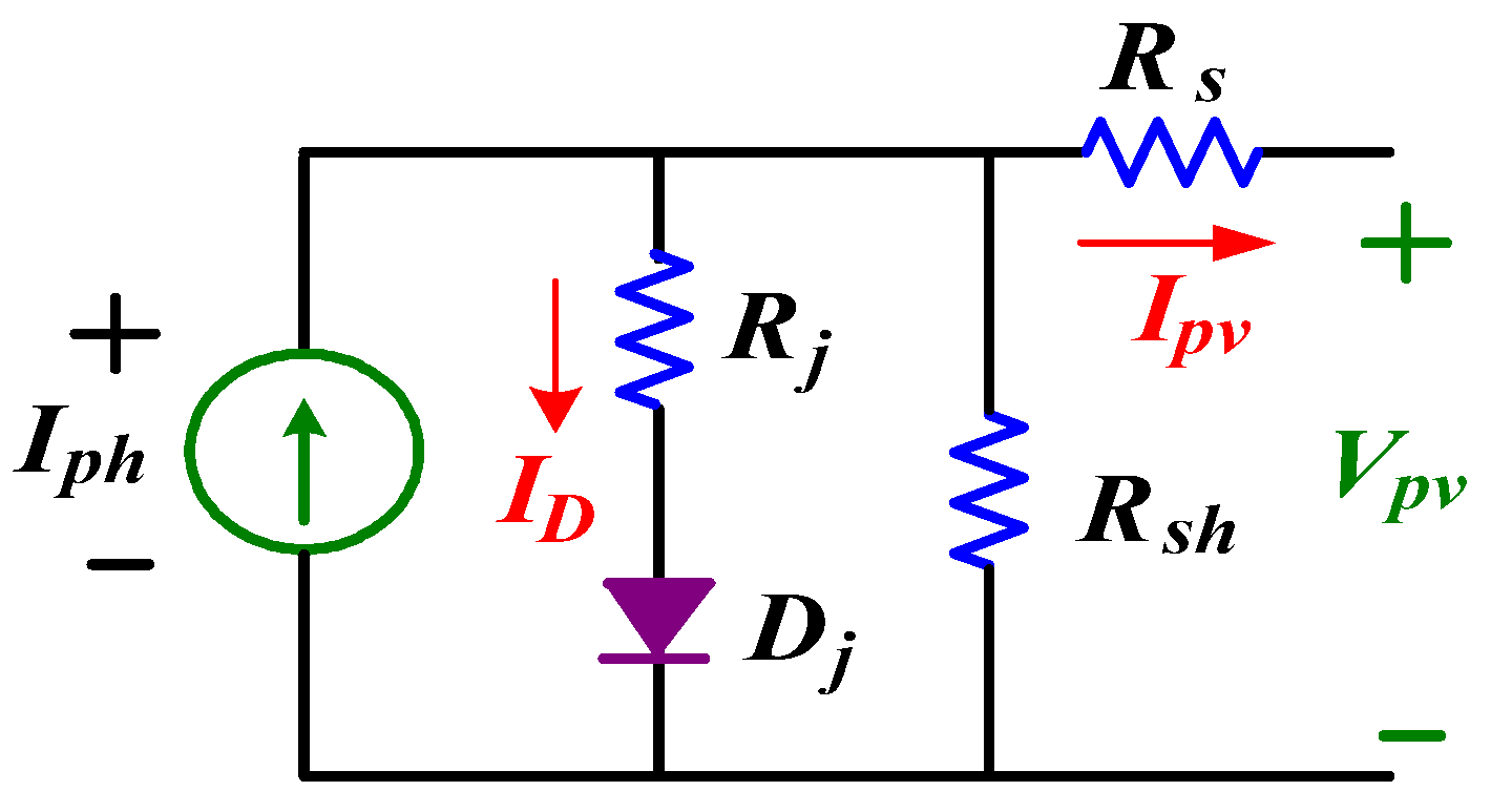
PV panels are composed of a number of PV modules, which are connected in series and/or in parallel [13]. Each PV cell is a p-n junction semi-conductor, converting solar energy into electricity. An equivalent circuit is shown in Figure 9, in which Iph stands for the cell photocurrent source, Dj represents the p-n junction, Rj, Rsh, and Rs are the p-n junction nonlinear impedance, intrinsic shunt resistance and intrinsic series resistance, respectively. Since a PV cell produces less than 3 watts at approximately 0.5 Vdc, PV cells must be connected in series-parallel configurations to produce enough power for high-power applications [14].From the Ipv-Vpv and Ppv-Vpv characteristics, the p-n junction and the equivalent circuit, the output current (IPV) and output power (Ppv) equations of PV panels can be expressed as follows:
or
and
where np is parallel number of PV cell, ns is series number of PV cell, Isat is reverse-saturation-current, Iph is output current of PV panel, q denotes the charges of an electron (1.6 × 10⁻¹⁹ coulomb), k is the Boltzmann’s constant (1.38 × 10⁻²³ J/°K), T is temperature of PV arrays (°K), and A represents ideality factor of the p-n junction (between 1 and 5) [15]. In addition, Isat is the reversed saturation current of the PV cells, which depends on temperature of PV arrays. It can be expressed by the following equation:
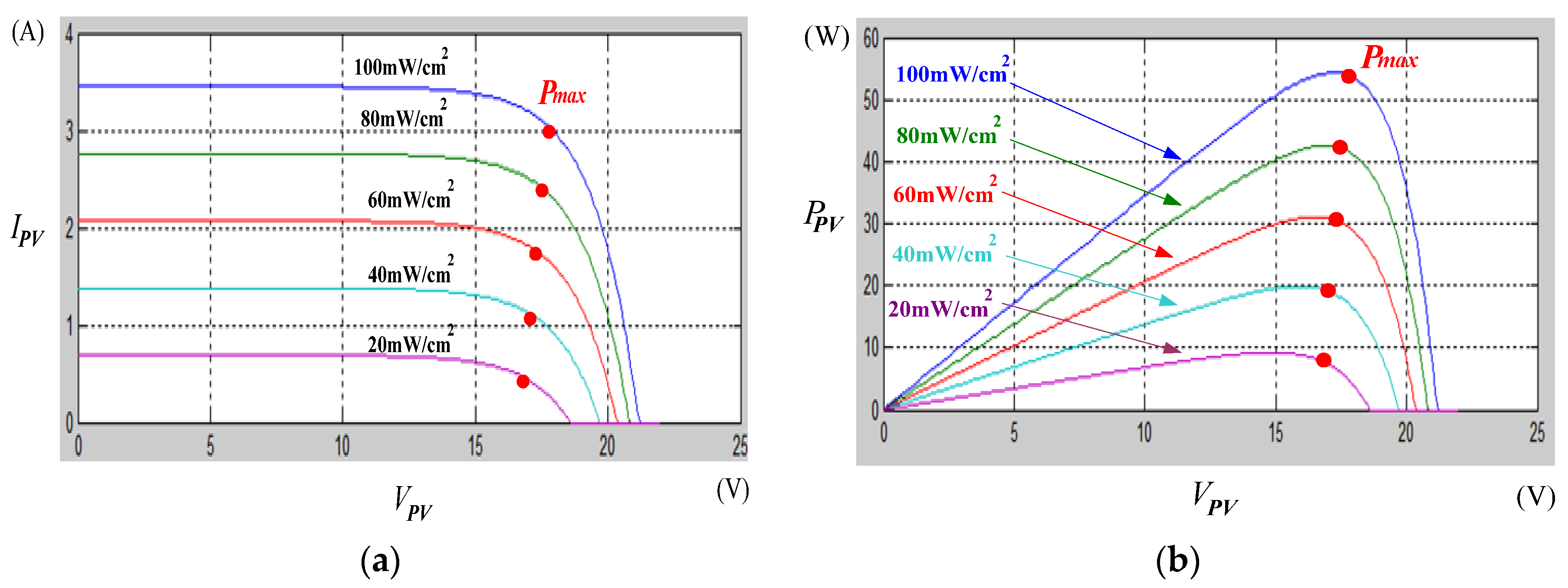
where Tr is the cell reference temperature, Irr is the corresponding reversed saturation current at Tr, and Egap stands for band-gap energy of the semiconductor in the PV cell. From the Equations (21)–(23), Ipv-Vpv and Ppv-Vpv curves can be obtained, as shown in Figure 10.
In Figure 10, it can be seen that the PV panels produce power only on illuminated isolation. There exists one operating point where the PV panels can generate their maximum output power Pmax. From Figure 10, it can be seen that a common inherent drawback of the PV panels is the intermittent nature of their power. The drawback tends to make the PV panels inefficient. However, by incorporating MPPT algorithms, the power transfer efficiency of the PV panels can be improved significantly.
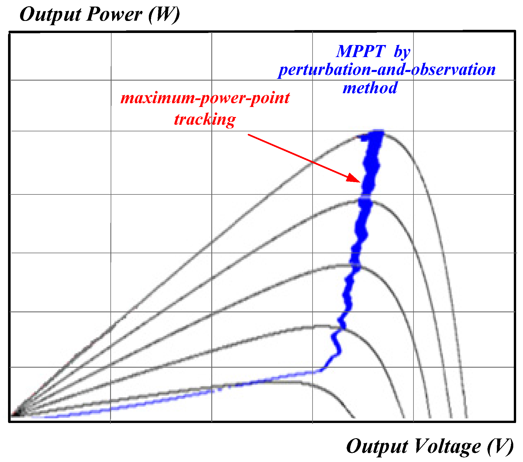
Based on the MPPT conception of the PV panels, a perturbation-and-observation method is widely used because it is easy to carry out and few measured parameters are required [16,17]. The conception circuit of the proposed soft-switching buck converter with MPPT algorithms is shown in Figure 11. In order to verify the performance and the feasibility of the perturbation-and-observation method, Figure 12 shows the MPPT curves of the PV panels by the simulation of Caspoc software, from which it can be seen that the optimum maximum-power-point of the PV panels can be precisely tracked by the perturbation-and-observation method.
4. Simulated and Experimental Results
To verify the performance of the proposed buck converter with soft-switching cells for the PV panel applications, its specifications are listed as follows:
- Voltage of PV array: Vpv = 60–80 Vdc,
- Output voltage of buck converter: Vo = 24 Vdc,
- Maximum output current of buck converter: Io = 4 A,
- Switching frequency (M1 and M2): fs = 50 kHz.
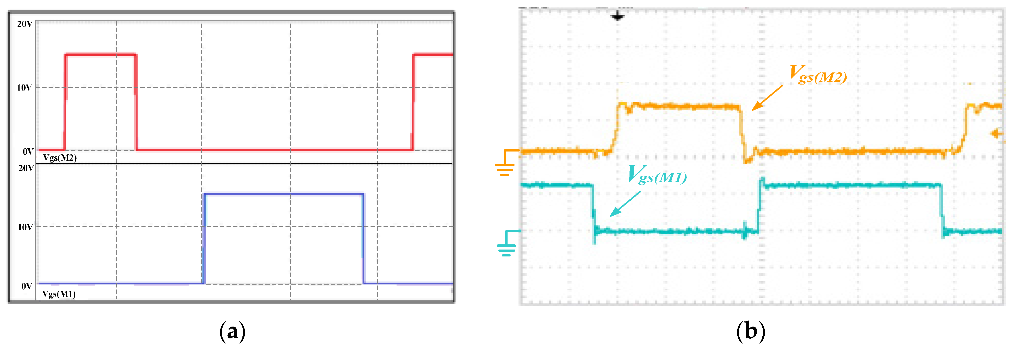
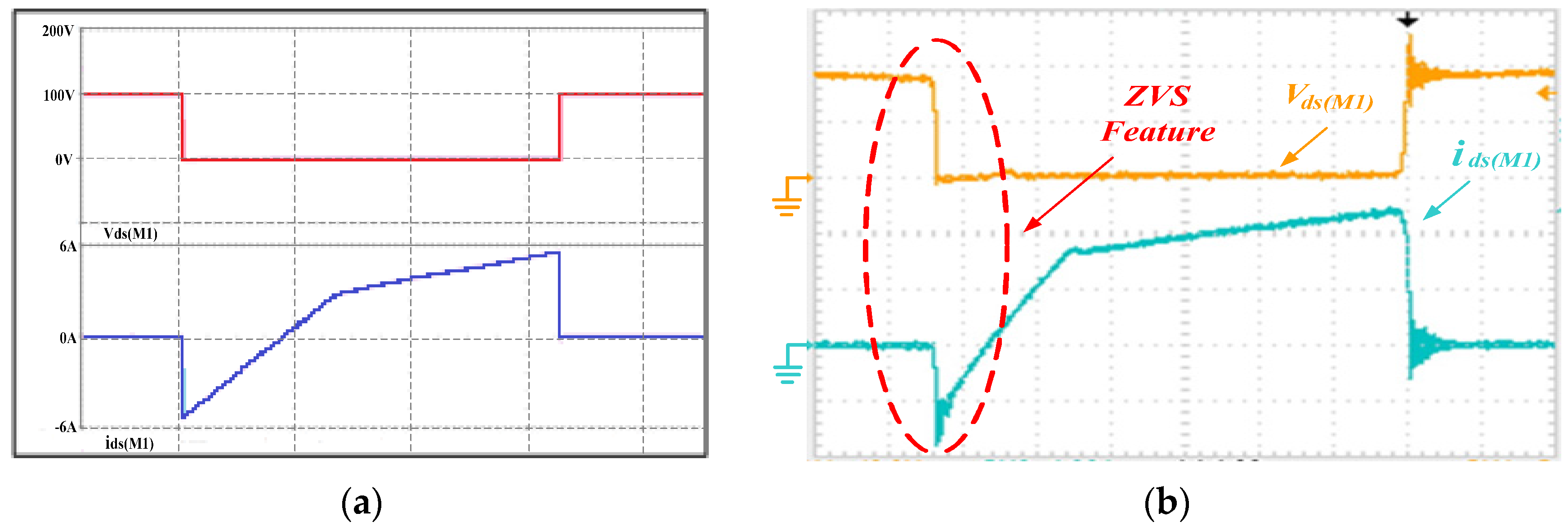
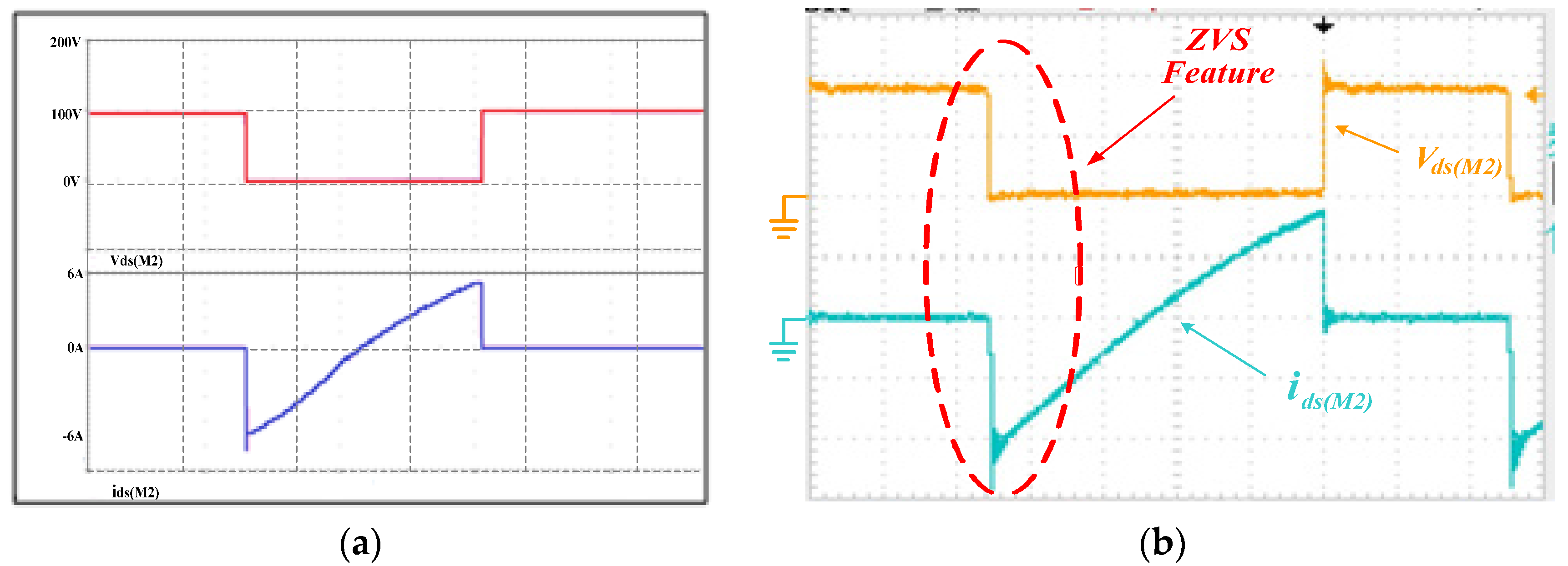
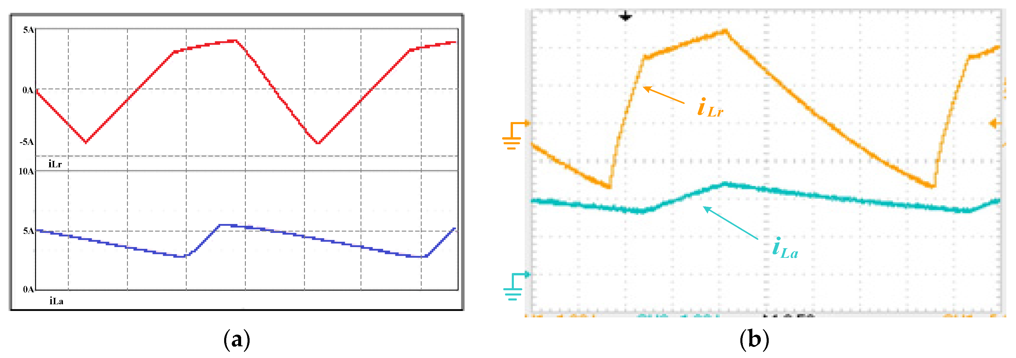
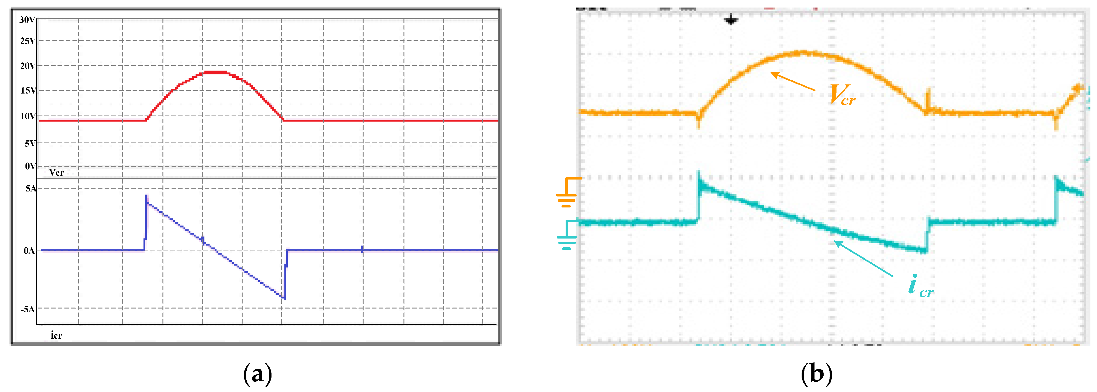
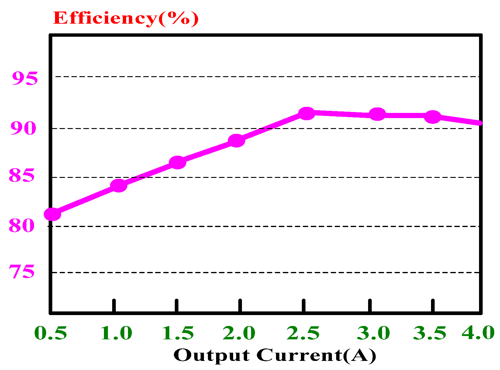
Figure 13 shows simulated and measured driving voltage waveforms of main and auxiliary switches (M1 and M2), in which they can be generated by a pulse-width-modulation (PWM) controller. Figure 14 shows simulated and measured voltage and current waveforms of main switch (M1), in which it can be seen that the main switch (M1) has a ZVS feature during turn-on transition. Figure 15 shows simulated and measured voltage and current waveforms of the auxiliary switch (M2), in which it also can be seen that the auxiliary switch (M2) has a ZVS feature during turn-on transition. Therefore, the switching losses of main switch (M1) and auxiliary switch (M2) can be eliminated during turn-on transition and conversion efficiency can be increased. Figure 16 shows simulated and measured current waveforms of resonant inductor (Lr) and stored inductor (La), in which it can be seen that their currents are operated in continuous conduction modes to provide enough energy of ZVS features. Figure 17 shows simulated and measured voltage waveforms of resonant capacitor (Cr), in which it can be seen that the voltage of the resonant capacitor has a resonant condition. Figure 18 shows simulated and measured voltage and current waveforms of a freewheeling diode (Da), in which it can be seen that the decreasing rate of the reverse-recovery current can be limited during turn-off transition. Figure 19 shows efficiency measurements of the proposed soft-switching buck converter, in which it can be seen that the maximum efficiency can reach as high as 91% under full load condition.
5. Conclusions
In this paper, a buck converter with soft-switching cells for PV panel applications is proposed. The main and auxiliary switches have ZVS features at the turn-on transition, and the reverse-recovery current of the freewheeling diode can be limited at the turn-off transition. Hence, the switching losses and EMI of the main and auxiliary switches can be reduced and conversion efficiency can be increased. In order to draw maximum power from PV panels, a simple perturbation-and-observation method is incorporated to realize maximum power conversion. Simulated and experimental results have verified the performance and efficiency of the prototype soft-switching buck converter. Therefore, the proposed soft-switching buck converter is relatively suitable for PV panel applications.
Acknowledgments
This work was supported by the National Science Council, Taiwan, under Grant No. MOST 104-2221-E-167-017.
Author Contributions
All of the authors contributed to publishing this paper. Cheng-Tao Tsai wrote the paper and Wang-Min Chen contributed to the editing work of the manuscript.
Conflicts of Interest
The authors declare that there is no conflict of interests regarding the publication of this paper.
References
- Tseng, S.; Tsai, C. Photovoltaic Power System with an Interleaving Boost Converter for Battery Charger Applications. Int. J. Photoenergy 2012, 2012, 1–15. [Google Scholar] [CrossRef]
- Patel, H.; Agarwal, V. MPPT Scheme for a PV-Fed Single-Phase Single-Stage Grid-Connected Inverter Operating in CCM with Only One Current Sensor. IEEE Trans. Energy Convers. 2009, 24, 256–263. [Google Scholar] [CrossRef]
- Chen, S.; Chen, J. Study ofthe Effect and Design Criteria of the Input Filter for Buck Converters with Peak Current-Mode Control Using a Novel System Block Diagram. IEEE Trans. Ind. Electron. 2008, 55, 3159–3166. [Google Scholar] [CrossRef]
- Tang, K.H.; Chao, K.H.; Chao, Y.W.; Chen, J.P. Design and Implementation of a Simulator for Photovoltaic Modules. Int. J. Photoenergy 2012, 2012, 1–8. [Google Scholar] [CrossRef]
- Wu, X.; Zhang, J.; Ye, X.; Qian, Z. Analysis and Derivations for a Family ZVS Converter Based on a New Active Clamp ZVS Cell. IEEE Trans. Ind. Electron. 2008, 55, 773–781. [Google Scholar] [CrossRef]
- Elasser, A.; Torry, D.A. Soft Switching Active Snubbers for DC/DC Converters. IEEE Trans. Power Electron. 1996, 11, 710–722. [Google Scholar] [CrossRef]
- Wang, H.; Chung, H.S.; Ioinovici, A. A New Concept of High-Voltage DC–DC Conversion Using Asymmetric Voltage Distribution on the Switch Pairs and Hybrid ZVS–ZCS Scheme. IEEE Trans. Power Electron. 2012, 27, 2242–2259. [Google Scholar] [CrossRef]
- Wang, C.M. A Novel ZCS-PWM Flyback Converter with a Simple ZCS-PWM Commutation Cell. IEEE Trans. Ind. Electron. 2008, 55, 749–757. [Google Scholar] [CrossRef]
- Chiang, C.; Chen, C. Zero-Voltage-Switching Control for a PWM Buck Converter under DCM/CCM Boundary. IEEE Trans. Power Electron. 2009, 24, 2120–2126. [Google Scholar] [CrossRef]
- Ilic, M.; Maksimovic, D. Interleaved Zero-Current-Transition Buck Converter. IEEE Trans. Ind. Appl. 2007, 43, 1619–1627. [Google Scholar] [CrossRef]
- Liu, K.H.; Lee, F.C. Zero-Voltage Switching Technique in DC/DC Converter. IEEE Trans. Power Electron. 1990, 5, 293–304. [Google Scholar] [CrossRef]
- Wang, C.M. New Family of Zero-Current-Switching PWM Converters Using a New Zero-Current-Switching PWM Auxiliary Circuit. IEEE Trans. Ind. Electron. 2006, 53, 768–777. [Google Scholar] [CrossRef]
- Wasynezuk, O. Dynamic Behavior of a Class of Photovoltaic Power Systems. IEEE Trans.Power Appar. Syst. 1983, PAS-102, 3031–3037. [Google Scholar] [CrossRef]
- Chao, K.H.; Chang, L.Y.; Liu, H.C. Maximum-Power-Point-Tracking Method Based on Modified Particle Swarm Optimization for Photovoltaic Systems. Int. J. Photoenergy 2013, 2013, 1–6. [Google Scholar] [CrossRef]
- Shen, C.; Tsai, C. Double-Linear Approximation Algorithm to Achieve Maximum-Power-Point-Tracking for PV Arrays. Energies 2012, 5, 1982–1997. [Google Scholar] [CrossRef]
- Kuo, Y.; Liang, T.; Chen, J. Novel Maximum-Power-Point-Tracking Controller for Photovoltaic Energy Conversion System. IEEE Trans. Ind. Electron. 2001, 48, 594–601. [Google Scholar]
- Hsiao, Y.; Chen, C. Maximum Power Tracking for Photovoltaic Power System. IEEE Trans. IAS 2002, 2, 1035–1040. [Google Scholar]
Figure 1.
Turn-on and turn-off transition waveforms: (a) MOSFET; (b) diode.

Figure 2.
Classification of DC-to-DC converters with soft-switching techniques.

Figure 3.
Illustration of soft-switching techniques: (a) ZVS and ZCS for a MOSFET; (b) limited decreasing rate of reverse-recovery current for a diode.
Figure 3.
Illustration of soft-switching techniques: (a) ZVS and ZCS for a MOSFET; (b) limited decreasing rate of reverse-recovery current for a diode.

Figure 4.
Circuit structure of the proposed buck converter with soft-switching cells for PV panel applications.
Figure 4.
Circuit structure of the proposed buck converter with soft-switching cells for PV panel applications.

Figure 5.
Simplified circuit diagram of the proposed soft-switching buck converter.

Figure 6.
Driving signals of active switches and conceptual current and voltage waveforms of key components.
Figure 6.
Driving signals of active switches and conceptual current and voltage waveforms of key components.

Figure 7.
Equivalent circuits of operating modes for the proposed soft-switching buck converter. (a) (Mode 1: t0<t<t1); (b) (Mode 2: t1<t<t2); (c) (Mode 3: t2<t<t3); (d) (Mode 4: t3<t<t4); (e) (Mode 5: t4<t<t5); (f) (Mode 6: t5<t<t6); (g) (Mode 7: t6<t<t7); (h) (Mode 8: t7<t<t8); (i) (Mode 9: t8<t<t9); (j) (Mode 10: t9<t<t10); (k) (Mode 11: t10<t<t11).


Figure 8.
Possible combinations of an active soft-switching cell in a typical buck converter: (a) type I; (b) type II; (c) type III.
Figure 8.
Possible combinations of an active soft-switching cell in a typical buck converter: (a) type I; (b) type II; (c) type III.


Figure 9.
Equivalent circuit of PV cell.

Figure 10.
PV panels with different insolations: (a) Ipv-Vpv curves; and (b) Ppv-Vpv curves.

Figure 11.
Conception circuit of the proposed soft-switching buck converter with MPPT algorithms. Pulse-width-modulation is (PWM).
Figure 11.
Conception circuit of the proposed soft-switching buck converter with MPPT algorithms. Pulse-width-modulation is (PWM).

Figure 12.
Simulation of perturbation-and-observation method by Caspoc software.

Figure 13.
Driving voltage waveforms of main and auxiliary switches (M1 and M2): (a) simulated results, (Vgs(M1): 10 V/div; Vgs(M2): 10 V/div; time: 2.5 μs/div); (b) experimental results. (Vgs(M1): 10 V/div; Vgs(M2): 10 V/div; time: 2.5 μs/div).
Figure 13.
Driving voltage waveforms of main and auxiliary switches (M1 and M2): (a) simulated results, (Vgs(M1): 10 V/div; Vgs(M2): 10 V/div; time: 2.5 μs/div); (b) experimental results. (Vgs(M1): 10 V/div; Vgs(M2): 10 V/div; time: 2.5 μs/div).

Figure 14.
Voltage and current waveforms of main switch M1: (a) simulated results, (Vds(M1): 100 V/div; ids(M1): 5 A/div; time: 2.5 μs/div); (b) experimental results. (Vds(M1): 50 V/div; ids(M1): 2.5 A/div; time: 2.5 μs/div).
Figure 14.
Voltage and current waveforms of main switch M1: (a) simulated results, (Vds(M1): 100 V/div; ids(M1): 5 A/div; time: 2.5 μs/div); (b) experimental results. (Vds(M1): 50 V/div; ids(M1): 2.5 A/div; time: 2.5 μs/div).

Figure 15.
Voltage and current waveforms of main switch M2: (a) simulated results, (Vds(M2): 100 V/div; ids(M2): 5 A/div; time: 2.5 μs/div); (b) experimental results. (Vds(M2): 50 V/div; ids(M2): 2.5 A/div; time: 2.5 μs/div).
Figure 15.
Voltage and current waveforms of main switch M2: (a) simulated results, (Vds(M2): 100 V/div; ids(M2): 5 A/div; time: 2.5 μs/div); (b) experimental results. (Vds(M2): 50 V/div; ids(M2): 2.5 A/div; time: 2.5 μs/div).

Figure 16.
Current waveforms of resonant and stored inductors: (a) simulated results, (iLr: 5 A/div; iLa: 5 A/div; time: 2.5 μs/div); (b) experimental results. (iLr: 2.5 A/div; iLa: 2.5 A/div; time: 2.5 μs/div).
Figure 16.
Current waveforms of resonant and stored inductors: (a) simulated results, (iLr: 5 A/div; iLa: 5 A/div; time: 2.5 μs/div); (b) experimental results. (iLr: 2.5 A/div; iLa: 2.5 A/div; time: 2.5 μs/div).

Figure 17.
Voltage and current waveforms of resonant capacitor: (a) simulated results, (Vcr: 10 V/div; icr: 5 A/div; time: 2.5 μs/div); (b) experimental results. (Vcr: 5 V/div; icr: 5 A/div; time: 2.5 μs/div).
Figure 17.
Voltage and current waveforms of resonant capacitor: (a) simulated results, (Vcr: 10 V/div; icr: 5 A/div; time: 2.5 μs/div); (b) experimental results. (Vcr: 5 V/div; icr: 5 A/div; time: 2.5 μs/div).

Figure 18.
Voltage and current waveforms of freewheeling diode: (a) simulated results, (VDa: 20 V/div; iDa: 5 A/div; time: 2.5 μs/div); (b) experimental results. (VDa: 50 V/div; iDa: 5 A/div; time: 2.5 μs/div).
Figure 18.
Voltage and current waveforms of freewheeling diode: (a) simulated results, (VDa: 20 V/div; iDa: 5 A/div; time: 2.5 μs/div); (b) experimental results. (VDa: 50 V/div; iDa: 5 A/div; time: 2.5 μs/div).

Figure 19.
Efficiency of the proposed soft-switching buck converter under full load condition.

© 2016 by the authors; licensee MDPI, Basel, Switzerland. This article is an open access article distributed under the terms and conditions of the Creative Commons by Attribution (CC-BY) license (http://creativecommons.org/licenses/by/4.0/).
Share and Cite
MDPI and ACS Style
Tsai, C.-T.; Chen, W.-M. Buck Converter with Soft-Switching Cells for PV Panel Applications. Energies 2016, 9, 148. https://doi.org/10.3390/en9030148
AMA Style
Tsai C-T, Chen W-M. Buck Converter with Soft-Switching Cells for PV Panel Applications. Energies. 2016; 9(3):148. https://doi.org/10.3390/en9030148
Chicago/Turabian StyleTsai, Cheng-Tao, and Wang-Min Chen. 2016. "Buck Converter with Soft-Switching Cells for PV Panel Applications" Energies 9, no. 3: 148. https://doi.org/10.3390/en9030148
Note that from the first issue of 2016, this journal uses article numbers instead of page numbers. See further details here.