
Catalysis-Free Growth of III-V Core-Shell Nanowires on p-Si for Efficient Heterojunction Solar Cells with Optimized Window Layer

Abstract
:1. Introduction
2. Experimental
3. Results and Discussion
4. Conclusions
Author Contributions
Funding
Institutional Review Board Statement
Informed Consent Statement
Data Availability Statement
Acknowledgments
Conflicts of Interest
References
- Kang, S.B.; Jeong, M.H.; Choi, I.Y.; Sohn, S.D.; Kim, S.H.; Shin, H.J.; Park, W.I.; Shin, J.C.; Song, M.H.; Choi, K.J. Self-assembled, highly crystalline porous ferroelectric poly(vinylidene fluoride-co-trifluoroethylene) interlayer for Si/organic hybrid solar cells. Nano Energy 2017, 41, 243–250. [Google Scholar] [CrossRef]
- Kang, S.B.; Kwon, K.C.; Choi, K.S.; Lee, R.; Hong, K.; Suh, J.M.; Im, M.J.; Sanger, A.; Choi, I.Y.; Kim, S.Y.; et al. Transfer of ultrathin molybdenum disulfide and transparent nanomesh electrode onto silicon for efficient heterojunction solar cells. Nano Energy 2018, 50, 649–658. [Google Scholar] [CrossRef]
- Kang, S.B.; Park, W.J.; Jeong, M.H.; Kang, S.H.; Yang, C.; Choi, K.J. Ambipolar Passivated Back Surface Field Layer for Silicon Photovoltaics. Adv. Funct. Mater. 2020, 30, 2004943. [Google Scholar] [CrossRef]
- Khan, M.E.; Khan, M.M.; Cho, M.H. Biogenic synthesis of a Ag-graphene nanocomposite with efficient photocatalytic degradation, electrical conductivity and photoelectrochemical performance. New J. Chem. 2015, 39, 8121–8129. [Google Scholar] [CrossRef]
- Naidi, S.N.; Khan, F.; Harunsani, M.H.; Tan, A.L.; Kim, Y.M.; Khan, M.M. Effect of Zr doping on photoantioxidant and antibiofilm properties of CeO2 NPs fabricated using aqueous leaf extract of Pometia pinnata. Bioprocess Biosyst. Eng. 2022, 45, 279–295. [Google Scholar] [CrossRef]
- del Alamo, J.A. Nanometre-scale electronics with III-V compound semiconductors. Nature 2011, 479, 317–323. [Google Scholar] [CrossRef]
- Vurgaftman, I.; Meyer, J.R.; Ram-Mohan, L.R. Band parameters for III-V compound semiconductors and their alloys. J. Appl. Phys. 2001, 89, 5815–5875. [Google Scholar] [CrossRef] [Green Version]
- Beyer, A.; Ohlmann, J.; Liebich, S.; Heim, H.; Witte, G.; Stolz, W.; Volz, K. GaP heteroepitaxy on Si(001): Correlation of Si-surface structure, GaP growth conditions, and Si-III/V interface structure. J. Appl. Phys. 2012, 111, 083534. [Google Scholar] [CrossRef]
- Bioud, Y.A.; Boucherif, A.; Myronov, M.; Soltani, A.; Patriarche, G.; Braidy, N.; Jellite, M.; Drouiri, D.; Ares, R. Uprooting defects to enable high-performance III-V optoelectronic devices on silicon. Nat. Commun. 2019, 10, 4322. [Google Scholar] [CrossRef]
- Doscher, H.; Supplie, O.; May, M.M.; Sippel, P.; Heine, C.; Munoz, A.G.; Eichberger, R.; Lewerenz, H.J.; Hannappel, T. Epitaxial III-V Films and Surfaces for Photoelectrocatalysis. Chemphyschem 2012, 13, 2899–2909. [Google Scholar] [CrossRef] [Green Version]
- Grassman, T.J.; Brenner, M.R.; Rajagopalan, S.; Unocic, R.; Dehoff, R.; Mills, M.; Fraser, H.; Ringel, S.A. Control and elimination of nucleation-related defects in GaP/Si(001) heteroepitaxy. Appl. Phys. Lett. 2009, 94, 232106. [Google Scholar] [CrossRef]
- Kratzer, P.; Penev, E.; Scheffler, M. First-principles studies of kinetics in epitaxial growth of III-V semiconductors. Appl. Phys. A-Mater. Sci. Processing 2002, 75, 79–88. [Google Scholar] [CrossRef] [Green Version]
- Tanabe, K.; Watanabe, K.; Arakawa, Y. III-V/Si hybrid photonic devices by direct fusion bonding. Sci. Rep. 2012, 2. [Google Scholar] [CrossRef] [PubMed]
- Bakkers, E.; Borgstrom, M.T.; Verheijen, M.A. Epitaxial growth of III-V nanowires on group IV substrates. Mrs Bull. 2007, 32, 117–122. [Google Scholar] [CrossRef]
- Duan, G.H.; Jany, C.; Le Liepvre, A.; Accard, A.; Lamponi, M.; Make, D.; Kaspar, P.; Levaufre, G.; Girard, N.; Lelarge, F.; et al. Hybrid III-V on Silicon Lasers for Photonic Integrated Circuits on Silicon. Ieee J. Sel. Top. Quantum Electron. 2014, 20, 6100213. [Google Scholar]
- Tomioka, K.; Tanaka, T.; Hara, S.; Hiruma, K.; Fukui, T. III-V Nanowires on Si Substrate: Selective-Area Growth and Device Applications. Ieee J. Sel. Top. Quantum Electron. 2011, 17, 1112–1129. [Google Scholar] [CrossRef]
- Gottschalch, V.; Wagner, G.; Bauer, J.; Paetzelt, H.; Shirnow, M. VLS growth of GaN nanowires on various substrates. J. Cryst. Growth 2008, 310, 5123–5128. [Google Scholar] [CrossRef]
- Mandl, B.; Keplinger, M.; Messing, M.E.; Kriegner, D.; Wallenberg, R.; Samuelson, L.; Bauer, G.; Stangl, J.; Holy, V.; Deppert, K. Self-Seeded Axio-Radial InAs-InAs1-xPx Nanowire Heterostructures beyond "Common" VLS Growth. Nano Lett. 2018, 18, 144–151. [Google Scholar] [CrossRef]
- Zhang, C.; Miao, X.; Chabak, K.D.; Li, X.L. A review of III-V planar nanowire arrays: Selective lateral VLS epitaxy and 3D transistors. J. Phys. D-Appl. Phys. 2017, 50, 393001. [Google Scholar] [CrossRef]
- Bae, M.H.; Kim, B.K.; Ha, D.H.; Lee, S.J.; Sharma, R.; Choi, K.J.; Kim, J.J.; Choi, W.J.; Shin, J.C. Non-Lithographic Growth of Core-Shell GaAs Nanowires on Si for Optoelectronic Applications. Cryst. Growth Des. 2014, 14, 1510–1515. [Google Scholar] [CrossRef]
- Lee, R.; Jo, M.H.; Kim, T.; Kim, H.J.; Kim, D.G.; Shin, J.C. Photoresponse and Field Effect Transport Studies in InAsP-InP Core-Shell Nanowires. Electron. Mater. Lett. 2018, 14, 357–362. [Google Scholar] [CrossRef]
- Shin, H.W.; Lee, S.J.; Kim, D.G.; Bae, M.H.; Heo, J.; Choi, K.J.; Choi, W.J.; Choe, J.W.; Shin, J.C. Short-wavelength infrared photodetector on Si employing strain-induced growth of very tall InAs nanowire arrays. Sci. Rep. 2015, 5, 10764. [Google Scholar] [CrossRef] [Green Version]
- Shin, J.C.; Kim, K.H.; Yu, K.J.; Hu, H.F.; Yin, L.J.; Ning, C.Z.; Rogers, J.A.; Zuo, J.M.; Li, X.L. InxGa1-xAs Nanowires on Silicon: One-Dimensional Heterogeneous Epitaxy, Bandgap Engineering, and Photovoltaics. Nano Lett. 2011, 11, 4831–4838. [Google Scholar] [CrossRef] [PubMed]
- Shin, J.C.; Lee, A.; Mohseni, P.K.; Kim, D.Y.; Yu, L.; Kim, J.H.; Kim, H.J.; Choi, W.J.; Wasserman, D.; Choi, K.J.; et al. Wafer-Scale Production of Uniform InAsyP1-y Nanowire Array on Silicon for Heterogeneous Integration. Acs Nano 2013, 7, 5463–5471. [Google Scholar] [CrossRef] [PubMed]
- O’Dwyer, C.; Szachowicz, M.; Visimberga, G.; Lavayen, V.; Newcomb, S.B.; Torres, C.M.S. Bottom-up growth of fully transparent contact layers of indium tin oxide nanowires for light-emitting devices. Nat. Nanotechnol. 2009, 4, 239–244. [Google Scholar] [CrossRef] [PubMed] [Green Version]
- Pandey, R.; Wie, C.H.; Lin, X.; Lim, J.W.; Kim, K.K.; Hwang, D.K.; Choi, W.K. Fluorine doped zinc tin oxide multilayer transparent conducting Oxides for organic photovoltaic’s Cells. Sol. Energy Mater. Sol. Cells 2015, 134, 5–14. [Google Scholar] [CrossRef]
- Rider, D.A.; Tucker, R.T.; Worfolk, B.J.; Krause, K.M.; Lalany, A.; Brett, M.J.; Buriak, J.M.; Harris, K.D. Indium tin oxide nanopillar electrodes in polymer/fullerene solar cells. Nanotechnology 2011, 22, 085706. [Google Scholar] [CrossRef]
- Kang, S.B.; Kim, J.H.; Jeong, M.H.; Sanger, A.; Kim, C.U.; Kim, C.M.; Choi, K.J. Stretchable and colorless freestanding microwire arrays for transparent solar cells with flexibility. Light Sci. Appl. 2019, 8, 121. [Google Scholar] [CrossRef] [Green Version]
- Yu, P.C.; Chang, C.H.; Su, M.S.; Hsu, M.H.; Wei, K.H. Embedded indium-tin-oxide nanoelectrodes for efficiency and lifetime enhancement of polymer-based solar cells. Appl. Phys. Lett. 2010, 96, 153307. [Google Scholar] [CrossRef] [Green Version]
- Li, S.Q.; Guo, P.J.; Zhang, L.X.; Zhou, W.; Odom, T.W.; Seideman, T.; Ketterson, J.B.; Chang, R.P.H. Infrared Plasmonics with Indium-Tin-Oxide Nanorod Arrays. Acs Nano 2011, 5, 9161–9170. [Google Scholar] [CrossRef]
- Lee, Y.J.; Yao, Y.C.; Yang, C.H. Direct electrical contact of slanted ITO film on axial p-n junction silicon nanowire solar cells. Opt. Express 2013, 21, A7–A14. [Google Scholar] [CrossRef] [PubMed]
- Foster, A.P.; Wilson, L.R. Design parameters for nanowire-planar tandem solar cells. Phys. Status Solidi A-Appl. Mater. Sci. 2013, 210, 425–429. [Google Scholar] [CrossRef]
- Guo, Y.N.; Xu, H.Y.; Auchterlonie, G.J.; Burgess, T.; Joyce, H.J.; Gao, Q.; Tan, H.H.; Jagadish, C.; Shu, H.B.; Chen, X.S.; et al. Phase Separation Induced by Au Catalysts in Ternary InGaAs Nanowires. Nano Lett. 2013, 13, 643–650. [Google Scholar] [CrossRef] [PubMed]
- Hocevar, M.; Immink, G.; Verheijen, M.; Akopian, N.; Zwiller, V.; Kouwenhoven, L.; Bakkers, E. Growth and optical properties of axial hybrid III-V/silicon nanowires. Nat. Commun. 2012, 3, 1266. [Google Scholar] [CrossRef] [Green Version]
- Holm, J.V.; Jorgensen, H.I.; Krogstrup, P.; Nygard, J.; Liu, H.Y.; Aagesen, M. Surface-passivated GaAsP single-nanowire solar cells exceeding 10% efficiency grown on silicon. Nat. Commun. 2013, 4, 1498. [Google Scholar] [CrossRef] [PubMed] [Green Version]
- Kim, Y.; Joyce, H.J.; Gao, Q.; Tan, H.H.; Jagadish, C.; Paladugu, M.; Zou, J.; Suvorova, A.A. Influence of nanowire density on the shape and optical properties of ternary InGaAs nanowires. Nano Lett. 2006, 6, 599–604. [Google Scholar] [CrossRef] [PubMed]
- Tomioka, K.; Yoshimura, M.; Fukui, T. A III-V nanowire channel on silicon for high-performance vertical transistors. Nature 2012, 488, 189–192. [Google Scholar] [CrossRef]
- Yang, T.; Hertenberger, S.; Morkotter, S.; Abstreiter, G.; Koblmuller, G. Size, composition, and doping effects on In(Ga)As nanowire/Si tunnel diodes probed by conductive atomic force microscopy. Appl. Phys. Lett. 2012, 101. [Google Scholar] [CrossRef]
- Jackson, J.B.; Kapoor, D.; Jun, S.G.; Miller, M.S. Integrated silicon nanowire diodes and the effects of gold doping from the growth catalyst. J. Appl. Phys. 2007, 102, 054310. [Google Scholar] [CrossRef]
- Kim, J.H.; Kang, S.B.; Yu, H.H.; Kim, J.; Ryu, J.; Lee, J.W.; Choi, K.J.; Kim, C.M.; Yi, C.H. Augmentation of absorption channels induced by wave-chaos effects in free-standing nanowire arrays. Opt. Express 2020, 28, 23569–23583. [Google Scholar] [CrossRef]
- Kelzenberg, M.D.; Boettcher, S.W.; Petykiewicz, J.A.; Turner-Evans, D.B.; Putnam, M.C.; Warren, E.L.; Spurgeon, J.M.; Briggs, R.M.; Lewis, N.S.; Atwater, H.A. Enhanced absorption and carrier collection in Si wire arrays for photovoltaic applications. Nat. Mater. 2010, 9, 239–244. [Google Scholar] [CrossRef] [PubMed]
- LaPierre, R.R.; Chia, A.C.E.; Gibson, S.J.; Haapamaki, C.M.; Boulanger, J.; Yee, R.; Kuyanov, P.; Zhang, J.; Tajik, N.; Jewell, N.; et al. III-V nanowire photovoltaics: Review of design for high efficiency. Phys. Status Solidi-Rapid Res. Lett. 2013, 7, 815–830. [Google Scholar] [CrossRef]
- Mariani, G.; Scofield, A.C.; Hung, C.H.; Huffaker, D.L. GaAs nanopillar-array solar cells employing in situ surface passivation. Nat. Commun. 2013, 4, 1497. [Google Scholar] [CrossRef] [PubMed] [Green Version]


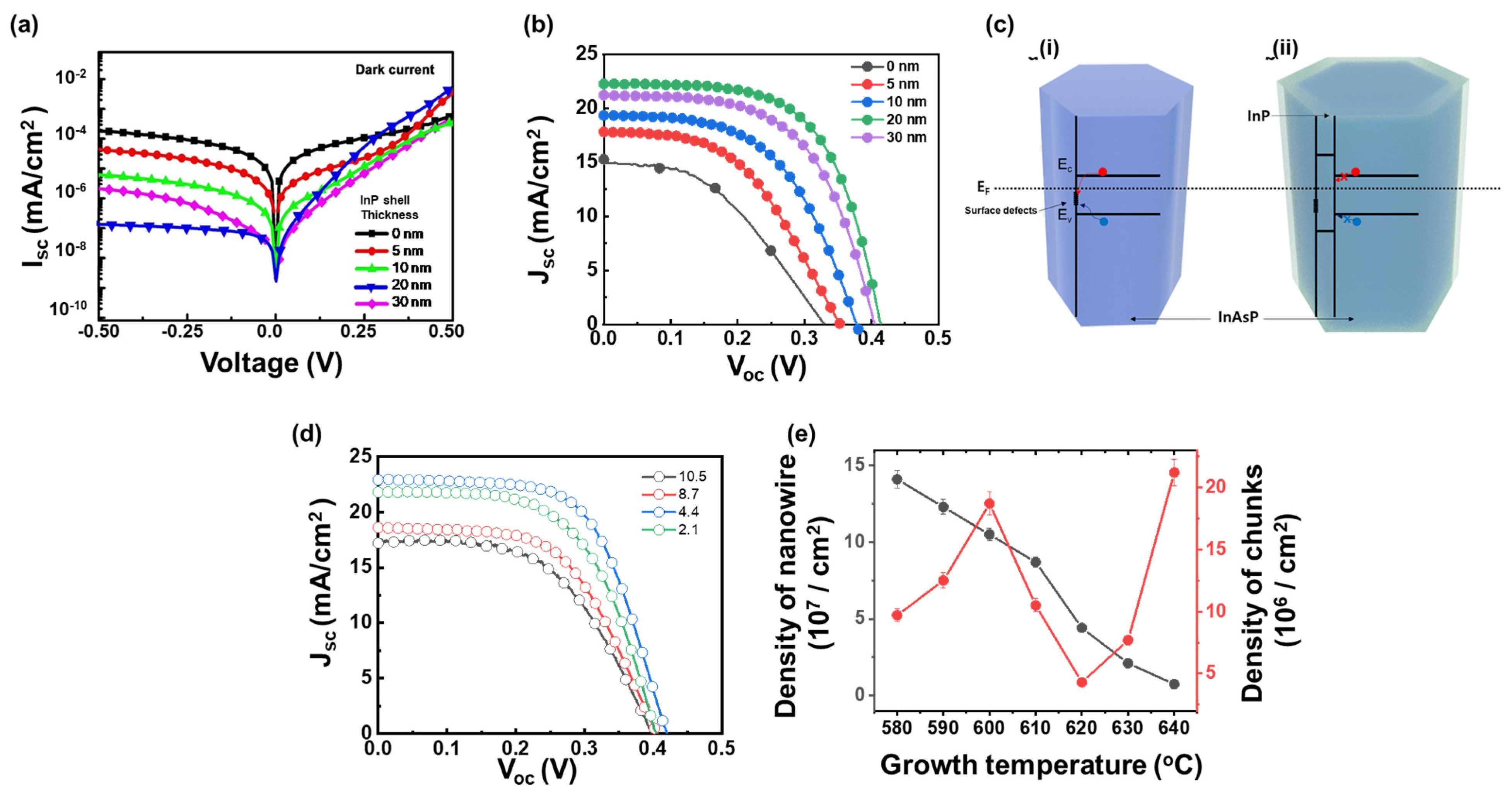
| InP Thickness | Jsc (mA/cm2) | Voc (mV) | FF | Eff. (%) |
|---|---|---|---|---|
| 0 | 15.43 | 325 | 42.1 | 2.11 |
| 5 | 17.80 | 353 | 48.2 | 3.15 |
| 10 | 19.33 | 378 | 53.4 | 3.91 |
| 20 | 22.25 | 423 | 61.4 | 5.70 |
| 30 | 21.22 | 405 | 57.8 | 5.05 |
| Density of Nanowire (10−7/cm2) | Jsc (mA/cm2) | Voc (mV) | FF | Eff. (%) |
|---|---|---|---|---|
| 10.5 | 16.95 | 398 | 50.8 | 3.39 |
| 8.7 | 18.58 | 406 | 56.0 | 4.08 |
| 4.4 | 22.90 | 420 | 61.6 | 5.89 |
| 2.1 | 21.80 | 404 | 58.2 | 5.17 |
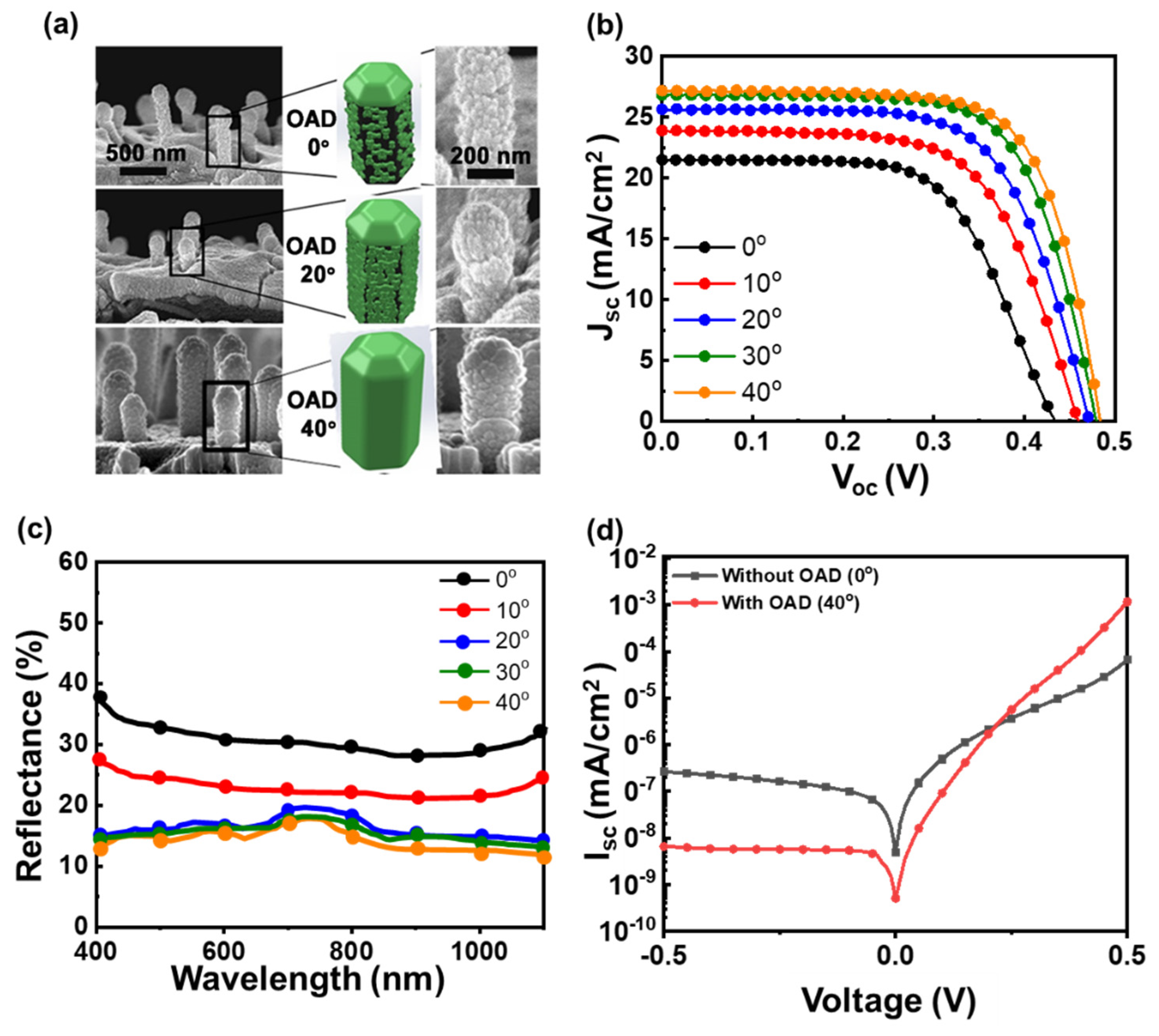
| Deposition Angle | Jsc (mA/cm2) | Voc (mV) | FF | Eff. (%) |
|---|---|---|---|---|
| 0 | 21.50 | 433 | 62.4 | 5.81 |
| 10 | 23.90 | 460 | 63.5 | 6.98 |
| 20 | 25.60 | 472 | 67.5 | 8.16 |
| 30 | 26.78 | 480 | 68.8 | 8.84 |
| 40 | 27.10 | 484 | 70.1 | 9.19 |
Publisher’s Note: MDPI stays neutral with regard to jurisdictional claims in published maps and institutional affiliations. |
© 2022 by the authors. Licensee MDPI, Basel, Switzerland. This article is an open access article distributed under the terms and conditions of the Creative Commons Attribution (CC BY) license (https://creativecommons.org/licenses/by/4.0/).
Share and Cite
Kang, S.B.; Sharma, R.; Jo, M.; Kim, S.I.; Hwang, J.; Won, S.H.; Shin, J.C.; Choi, K.J. Catalysis-Free Growth of III-V Core-Shell Nanowires on p-Si for Efficient Heterojunction Solar Cells with Optimized Window Layer. Energies 2022, 15, 1772. https://doi.org/10.3390/en15051772
Kang SB, Sharma R, Jo M, Kim SI, Hwang J, Won SH, Shin JC, Choi KJ. Catalysis-Free Growth of III-V Core-Shell Nanowires on p-Si for Efficient Heterojunction Solar Cells with Optimized Window Layer. Energies. 2022; 15(5):1772. https://doi.org/10.3390/en15051772
Chicago/Turabian StyleKang, Sung Bum, Rahul Sharma, Minhyeok Jo, Su In Kim, Jeongwoo Hwang, Sang Hyuk Won, Jae Cheol Shin, and Kyoung Jin Choi. 2022. "Catalysis-Free Growth of III-V Core-Shell Nanowires on p-Si for Efficient Heterojunction Solar Cells with Optimized Window Layer" Energies 15, no. 5: 1772. https://doi.org/10.3390/en15051772