1. Introduction
In the last decade, the interests of scientific, industrial, and political communities focused on environmental issues, in particular on future catastrophic climate scenarios currently foreseen with temperature increases of up to 2 °C [
1,
2]. Therefore, several efforts of these communities to find new solutions to improve greenhouse gas reduction and decarbonize of energy sources have been detected. In detail, the European Commission launched the European Green Deal [
3] that provides for a substantial reduction in polluting emissions by 2050 with policies that encourage member states to adopt innovative and advanced solutions. Many efforts of scientific and industrial communities have focused on the research and development of innovative technologies to increase the penetration of renewable sources into the production of electrical energy, trying to satisfy the goals of sustainable development and energy savings. In detail, the power electronics technologies, owing to their features and potentiality, play a fundamental role in this scenario.
At present, most applications of energy production from renewable sources employ traditional two-level Voltage Source Inverters (VSIs) that present several operative limitations for greater penetration of renewable energy sources into the electrical grid, such as high harmonic content and control flexibility. Indeed, the main performance indicator of a power converter is the harmonic distortion in the output voltages. For this reason, in order to evaluate the harmonic distortion of a VSI and its impact in different fields of applications, several indices have been proposed in the literature, as discussed in [
4]. Moreover, currently, a new concept of the power conversion systems, called “Smart Inverters”, is developing, in which inverters perform additional functions (e.g., self-governing, self-adapting, and self-healing features), as reported in [
5].
In this context, Multilevel Power Inverters (MPIs) are a promising solution since they present, with respect to the traditional three-phase two-level inverters, reduced harmonic content in the output voltages, lower voltage stress in the power components, and reduced Electromagnetic Interference (EMI) [
6,
7]. Therefore, multilevel power inverters, because of these features, represent a valid solution in many fields of application where high performance is required [
8,
9,
10].
According to [
11,
12], the MPIs can be classified into single DC source and multiple DC sources. The classical single DC source multilevel inverters are Neutral-Point Clamped (NPC), Flying Capacitor Inverter (FCI), and Modular Multilevel Converter (MMC). The Cascaded H-Bridge Multilevel Inverter (CHBMI) is a multiple DC sources type. Moreover, there are new reduced switch count topologies that have a common objective of reducing the number of the power components to increase the reliability of the converter. Nevertheless, all of these topologies generally present higher hardware complexity and a lower or absent modular feature.
Among classical and new topology structures of MPIs, the CHBMI stands out in particular for its modular structure, high flexibility, and intrinsically fault-tolerant capability. Moreover, in many applications where the DC sources are naturally separated, e.g., Photovoltaic (PV) systems and vehicles propulsion, the CHBMI is particularly fascinating since it allows easy expansion and reconfiguration of the PV plant or the battery package, also in fault condition [
13,
14]. Furthermore, the CHBMI performance is a function of the modulation strategy employed, especially regarding the efficiency and the harmonic content in the output voltage and current waveforms [
15,
16]. Moreover, the modulation strategy choice is also fundamental for the optimal and economic design of LCL filters, especially for grid-connected applications [
17].
The typical modulation strategies employed for CHBMI are the Multicarrier Pulse Width Modulations (MC PWM) that are an evolution of conventional PWM modulation strategies employed for traditional VSIs. In detail, the main features of these modulation strategies are simple implementation in the common electronic devices (e.g., microcontrollers and FPGA systems) and control flexibility owing to the simple adaptation in closed-loop controls. Moreover, the MC PWM schemes allow for obtaining a good response in terms of the harmonic distribution in the frequency domain because the low order harmonics are absent and significant harmonics start at the switching frequency. Indeed, there are several kinds of MC PWM that present different behavior and impact on CHBMI performance in terms of harmonic content and conversion efficiency. Furthermore, advanced multicarrier PWM modulation strategies are proposed in the literature. By way of example, in [
18], a modified MC PWM scheme, based on the phase shifted as carrier pattern, for a five-level three-phase CHBMI has been proposed. The authors aim is to improve the lifetime and reliability by reducing the switching losses through clamped modulation signals where each leg conducts switching operations at different frequencies. Although a power loss reduction was demonstrated through experimental tests, a complete analysis that takes into account the impacts on the harmonic distortion and conversion efficiency, in different operation conditions, is missing. In [
19], the authors propose a modified level-shifted pulse width modulation to improve the fault-tolerant capabilities of CHBMI. In this case, the authors demonstrate that the proposed method allows for balancing line voltage and currents in case of a fault of the converter. Nevertheless, the impact of the proposed method in terms of harmonic distortion and efficiency is missing.
In high power and medium-high voltage applications, low-switching frequency modulation schemes such as Selective Harmonic Elimination (SHE) and Selective Harmonic Mitigation (SHM) algorithms are used to obtain high converter efficiency [
20]. These algorithms allow for elimination or mitigation of low-order voltage harmonics by using a set of nonlinear transcendental equations systems, in which the order depends on the number of converter voltage levels. In the literature, different approaches are proposed to overcome and simplify the applications of the SHE and SHM algorithms [
21,
22,
23]. Nevertheless, these algorithms provide good performance when converter voltage levels are high, in which it is possible to eliminate or mitigate a greater number of the harmonics. By changing point of view, SHE and SHM algorithms are hardly used because of their high computational costs; extensive electronic hardware resources are required for real-time implementation.
Another interesting method to drive a converter is the Space Vector PWM (SVPWM) that, as well known, is particularly adapted in electric drives and traction applications. The Space Vector PWM (SVPWM) strategies are widely adopted for good DC-link voltage utilization, for flexibility in switching states selection, and for lower THD, as discussed in [
24]. According to [
25], a novel SVPWM for an electrical drive system-based Permanent Magnet Synchronous Machine (PMSM) fed by CHBMI has been proposed with the purpose of reducing the computational complexity. The authors have demonstrated a significant reduction of the switching losses, but the analysis does not account for the harmonic distortion impact in the motor with the proposed method.
Although most of the contributions in the literature are focused on the study and definition of new modulation schemes to improve the performance of multilevel converters, there are few comparative studies focused on multilevel converter performance as a function of modulation technique and its parameters such as switching frequency and dead-time, especially regarding the CHBMI circuit topology.
In [
26], the authors study the main difference between space vector modulation and carrier-based PWM modulation schemes by analyzing the output voltage harmonic content of a five-level three-phase NPC inverter. Additionally, in this work, the study is focused on the harmonic distortion while a comparison between the conversion efficiency in different operation conditions is missing.
In [
27], the energy performance of various types of voltage and current source inverters, including multilevel inverters, is examined and the inverter efficiency is evaluated for fixed switching frequency value as a function of output power or modulation index.
In [
28], the authors compare the performance of a modular multilevel single-delta bridge-cell (SDBC) inverter, for utility-scale grid-tied photovoltaic applications, in terms of power-balancing capability and harmonic performance by using phase-shifted PWM and level-shifted PWM. Additionally, in this case, the analysis was carried out for different load conditions but without varying the switching frequency.
In [
29], the authors present a new cascaded H-bridge multilevel inverter configuration and its performance in terms of total harmonic distortion, distortion factor, and power losses, which are analyzed as a function of the modulation index.
Some conference papers [
30,
31] address the effect of switching frequency on multilevel inverter performance in terms of harmonic content, although not extensively and they do not investigate the effects on inverter efficiency. In [
32], CHBMI efficiency and voltage waveforms THD are evaluated by varying the switching frequency for fixed amplitude modulation index; only two MC PWM schemes are compared and the analysis is performed in simulation. In [
33,
34], switching and conduction losses in CHBMI are analyzed, owing to the implementation of a power loss model; SHE soft switching and LS-SPWM control techniques are compared. In [
35,
36], the impact of CHBMI in powertrains is evaluated; in detail, switching losses, torque ripple, and THD are evaluated by varying the number of CHBMI levels per phase and the amplitude modulation index; PS PWM control technique is chosen and the switching frequency is fixed.
In [
37], an advanced power loss model is developed; IGBT-based traditional inverter, IGBT-based CHBMI and SiC MOSFET-based CHBMI are compared in order to evaluate the impact of different inverter topologies and different fully controlled switching devices technologies on electric vehicle performance and cost. Only the PS-PWM scheme is taken into account and the switching frequency is fixed. In [
38], the switching loss model is developed, and LS PWM, PS PWM, and SHE control schemes are compared for fixed switching frequency.
As can be seen, regarding the converter efficiency, several analyses have been carried out on inverter losses and voltage THD; however, on a side, switching frequency is treated as a fixed parameter, on the other, only a small number of PWM control strategies are taken into account and compared for the same conditions. In addition, most of the cited works are carried out only in the simulation environment.
In summary, it is possible to claim that the switching frequency effects in the harmonic distortion and conversion efficiency have been rarely investigated and reported in the literature. In particular, a detailed comparison among the commonly used MC PWM schemes and their behavior, in terms of the conversion efficiency and harmonic distortion, are missing in a unique work. Indeed, if on the one hand, the increase in the switching frequency determines a shift in the voltage harmonic spectrum, with consequent advantages in terms of power quality and sizing of the filtering system, then, on the other hand, it determines a reduction in the inverter efficiency. In some grid-connected applications, in order to reduce the impact of the grid–interface filter size, in terms of inductance and capacitance, high switching frequencies are chosen to result in a reduction of the conversion efficiency. Therefore, an extended performance analysis of multilevel inverters as a function of switching frequency can be of considerable importance for identifying optimal working conditions of the inverter, depending on the application, both in terms of harmonic distortion and efficiency.
This paper aims to perform an extended and experimental analysis of a three-phase five-level CHBMI performance in terms of efficiency and harmonic content when ten MC PWM modulation strategies are employed. In detail, three different carrier dispositions, one phase-shifted and one suppressed carrier arrangement modulation strategies have been considered, and, for each one, the sinusoidal and switching frequency optimal modulation signals have been employed. Moreover, in this analysis, the CHBMI performances are evaluated by varying, for each modulation strategy, the modulation index and the switching frequency. The implementation of the modulation strategies and, therefore, the control of CHBMI are carried out on NI System On Module sbRIO-9651 (SOM sbRIO-9651) that is a control board designed and distributed for power electronics and drive control applications. This control board presents an FPGA control unit and a real-time processor that can be programmed separately with consequent benefits in terms of control flexibility. Moreover, the SOM sbRIO-9651 can be programmed in the LabVIEW environment with the benefits of graphical language [
39]. Therefore, the results obtained can be usefully employed for the optimal choice of modulation strategy of CHBMI according to the application requirements.
The paper consists of the following sections:
Section 2 presents the MC PWM modulation strategies considered and their main features;
Section 3 describes the implementation on the SOM sbRIO-9651 control board and computational cost analysis;
Section 4 presents the test bench set-up and the CHBMI prototype analyzed;
Section 5 presents the experimental investigations carried out and the results obtained.
2. Overview of Multicarrier PWM Schemes for Three-Phase Five-Level CHBMI
In this section, a brief description and comparison of the main multicarrier PWM schemes considered in this work are reported. In detail, the comparison is carried out by taking into account the harmonic distribution in function of the switching frequency, the DC power absorption among the voltage levels, and the implementation resources required.
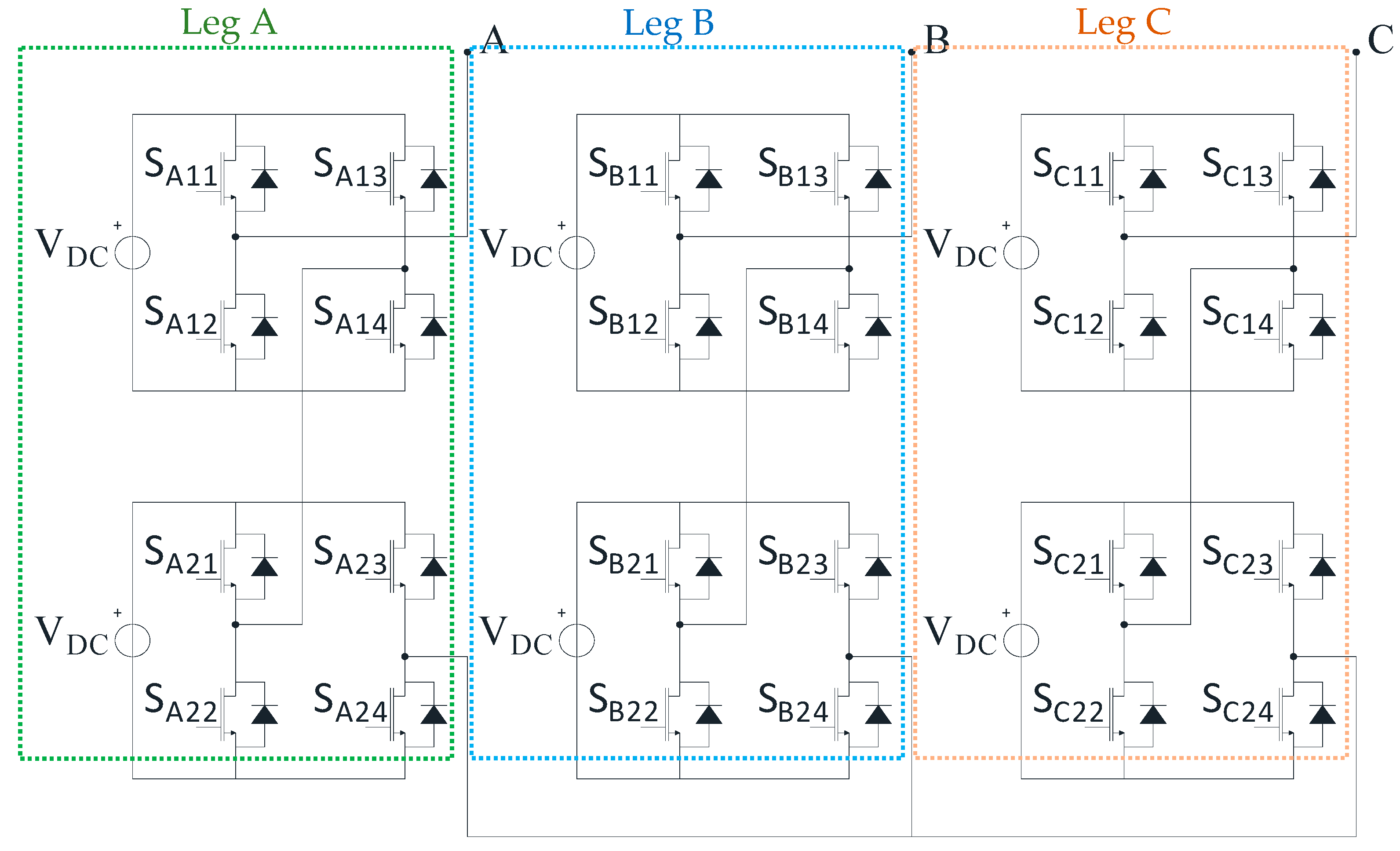
In detail, the circuit diagram of a three-phase five-level CHBMI is shown in
Figure 1.
As shown in
Figure 1, a three-phase five-level CHBMI converter is composed of six H-bridge modules that can be easily changed in case of a fault. Moreover, in the case of a fault of a power component or an H-bridge module inside a leg of the converter, the CHBMI can be reconfigured to work with reduced voltage, thus maintaining continuous operation.
Generally, the performance of the converter depends by the modulation schemes in terms of harmonic distortion. In particular, Multi-Carrier Pulse Width Modulations (MC PWM) are commonly used in many fields of applications due to the simple implementation in the common electronic devices (microcontroller or FPGA) and the good response in terms of the harmonic content that allows for easy voltage and current filtering. Moreover, owing to the new technologies of the power components that allow increasing the operation speeds, the MC PWM is attracting growing interest in industrial applications.
According to [
11], the MC PWM can be classified in Carrier Disposition (CD) scheme and Phase Shifted (PS) scheme. Generally, these modulation strategies represent an evolution of the classical PWM scheme for three-phase three or two-level converters in which are present modulations and carrier signals. In particular, by comparing in real-time modulation signal and carrier signal, the gate commands are generated for each power component.
The CD schemes, called also level shifted modulations, are composed with a number of the carrier signals
nC,CD equal to:
where
nl is the number of the voltage levels of the converter. Thus, for a five-level converter, a CD scheme is composed of four carrier signals. In the CD scheme, the four carrier signals present the same time variable profile, with identical peak-to-peak amplitude, but are amplitude-shifted with a nonzero average value and the phase among the carrier signals can be equal to 0 or ±π.
In the phase disposition function among the carrier signals, there are three types of CD modulation schemes:
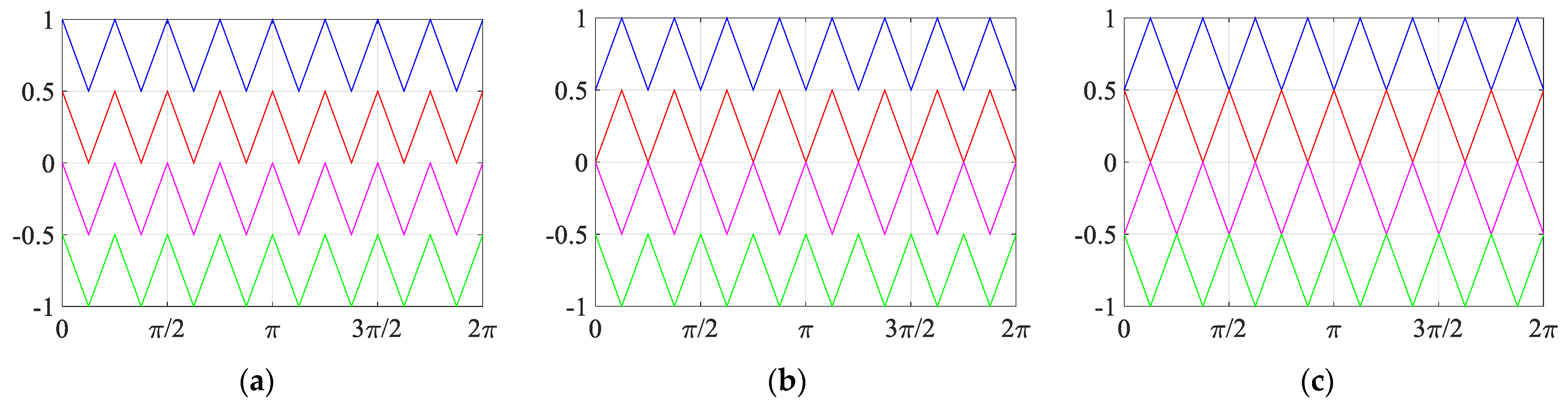
In the PD scheme, all carrier signals have the same phase. In the POD scheme, the carrier signals have the same phase, two by two. In the APOD scheme, all carrier signals are in phase-opposition. The carrier patterns CD-based in a period of the modulation signals are shown in
Figure 2.
In terms of the harmonic distribution in the frequency domain, the CD schemes present similar harmonic distribution in which the harmonics are centered at the switching frequency and integer multiplies, similar to a traditional two- or three-level inverter. Moreover, the commutations number is limited because each H-bridge works in an alternative way and the DC power absorption is not uniform among the voltage levels.
The PS scheme is composed of a number of the carrier signals
nC,PS equal to:
that is half of the CD schemes. Moreover, the carrier signals in the PS scheme present the same peak-to-peak amplitude, an average value equal to zero, and the carrier signals are shifted of an angle given by:
where
i is the
ith H-bridge and
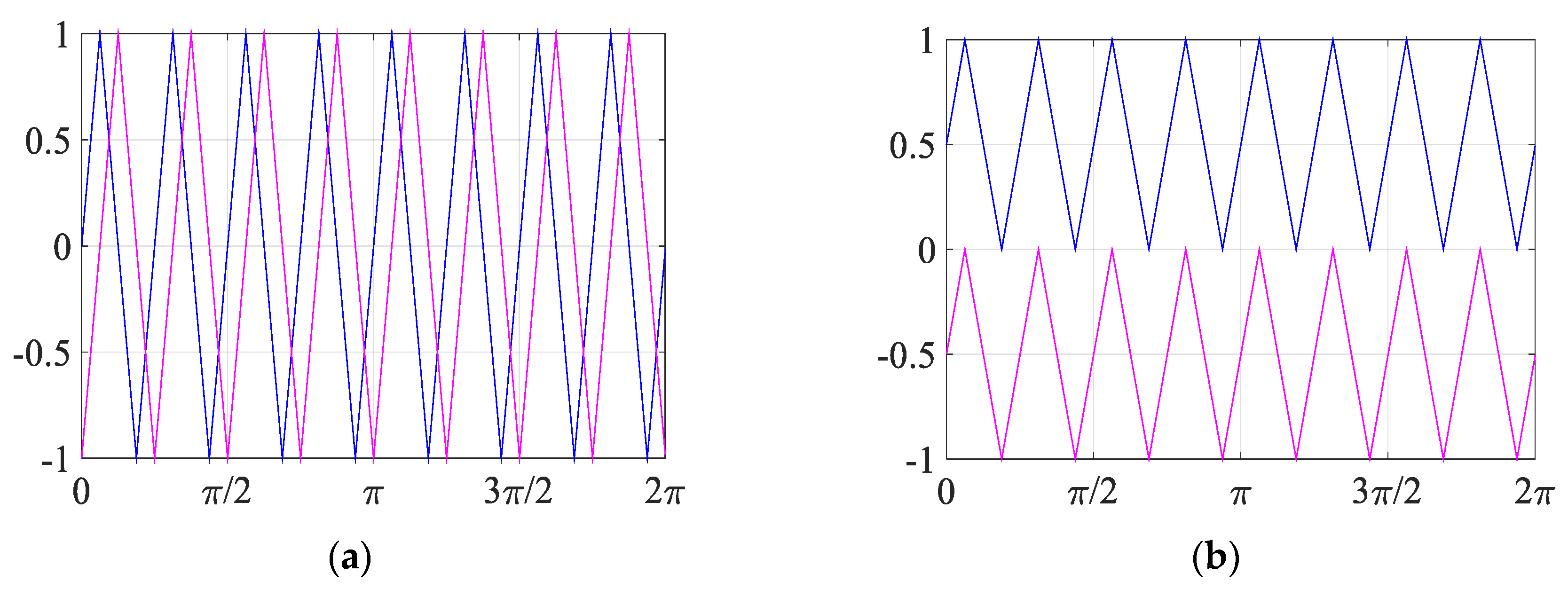
N is the number of the H-bridges cascaded connected. Thus, for a three-phase five-level CHBMI, the PS scheme is composed of two carrier signals that are shifted by an angle equal to 90°. The carrier pattern PS-based is shown in
Figure 3a.
It should be noted that with PS modulation each H-bridge works similar to a classical tree-level single-phase inverter. In this way, each H-bridge module absorbs the same DC power from the sources and the commutations number in each PWM period is four times the commutations number of CD schemes. Therefore, a shifted harmonic distribution towards the high frequency is expected with respect to the CD schemes and, in particular, the first voltage harmonics are centered at a frequency equal to:
where
fsw is the switching frequency. Thus, by using the PS scheme the converter works with a virtual frequency
fh that depends on the voltage levels
nl. In detail, for a five-level three-phase CHBMI, the first voltage harmonics are centered at a frequency four times that of the switching frequency. Nevertheless, a major commutations number generates an increase of the switching losses.
A hybrid modulation scheme is called Suppressed Carried Arrangement Modulation (SCAMOD). As described in [
40,
41], the SCAMOD is carried out by using the same concept of the level-shifted schemes, and the converter is controlled the same as in the PS scheme. The number of the carrier signals is the same as the PS scheme and the modulation pattern is made similar to a phase disposition scheme. Thus, for a three-phase five-level, the SCAMOD pattern is composed of two carrier signals with the same phase and the same peak-to-peak amplitude but are amplitude-shifted with a non-zero average value. The carrier pattern PS-based is shown in
Figure 3b.
In terms of the harmonic distribution in the frequency domain, the SCAMOD present an intermediate behavior between CD and PS carrier patterns. In particular, the first voltage harmonics are centered at a frequency equal to:
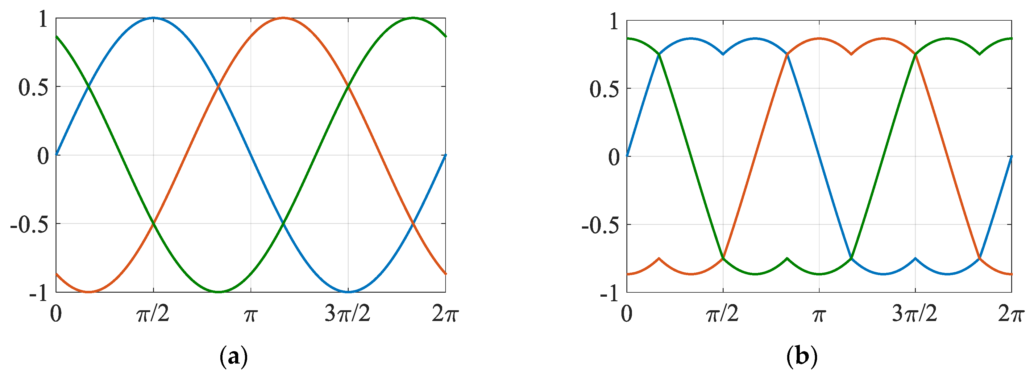
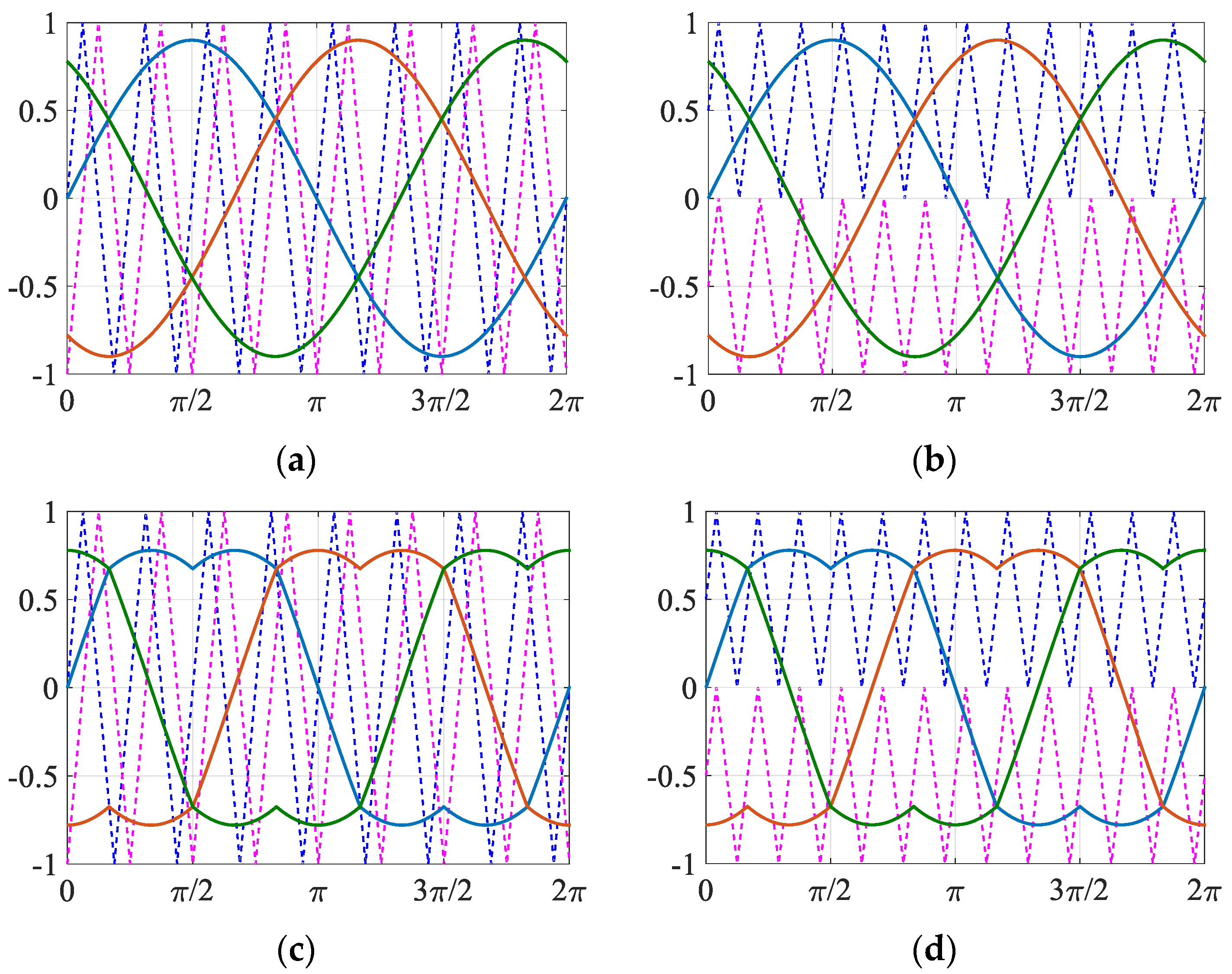
that is half of the PS scheme. Moreover, the SCAMOD scheme allows for uniforming the DC power absorption between the sources such as the PS scheme. Furthermore, the performance of the converter is affected by the waveform of the modulation signals. In detail, the common waveform modulation signals are sinusoidal and Switching Frequency Optimal (SFO) as shown in
Figure 4a,b, respectively. The first is commonly used in grid-connected applications and the second is commonly used in electrical drive applications.
The SFO modulation signals for three-phase converters can be expressed as:
where
va,
vb,, and
vc are the sinusoidal modulation signals, and
voffset is an offset signal determined as:
In detail, the voffset is a signal with a triangle waveform and a frequency equal to three times the fundamental voltage harmonic.
According to [
42], the SFO modulation signals allow for obtaining the same overall harmonic content of a Space Vector PWM (SV PWM) and the modulation index can be extended up to 1.15.
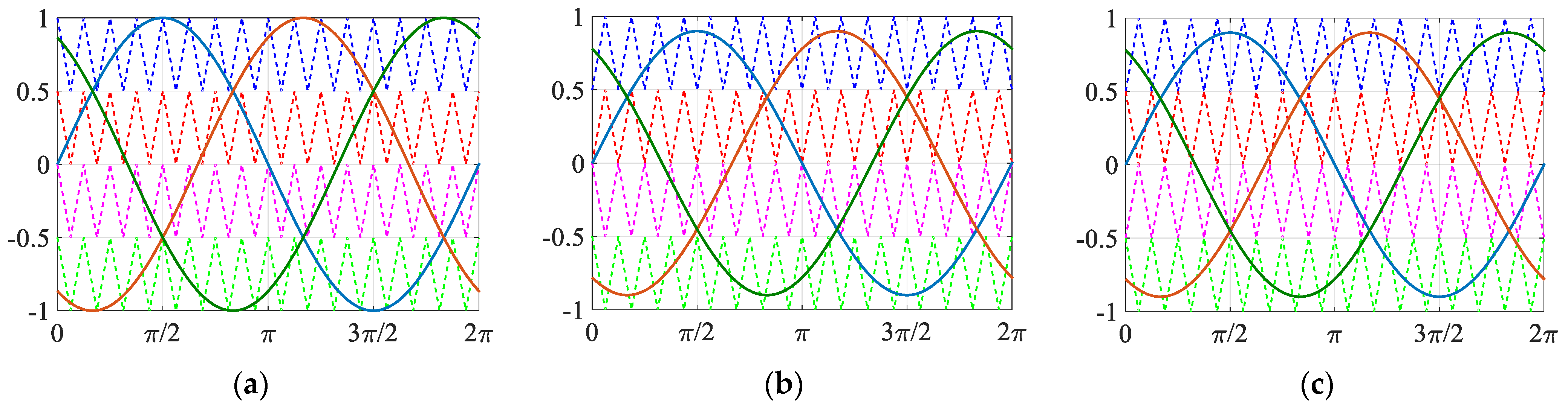
As previously described, this work aims to analyze the performance of the converter with the commonly used MC PWM schemes. Thus, the CD-based modulation schemes adopted and tested in this work follow:
Sinusoidal Phase Disposition—SPD (
Figure 5a);
Sinusoidal Phase Opposition Disposition—SPOD (
Figure 5b);
Sinusoidal Alternative Phase Opposition Disposition—SAPOD (
Figure 5c);
Switching Frequency Optimal Disposition—SFOPD (
Figure 5d);
Switching Frequency Optimal Phase Opposition Disposition—SFOPOD (
Figure 5e);
Switching Frequency Optimal Alternative Phase Opposition Disposition—SFOAPOD (
Figure 5f).
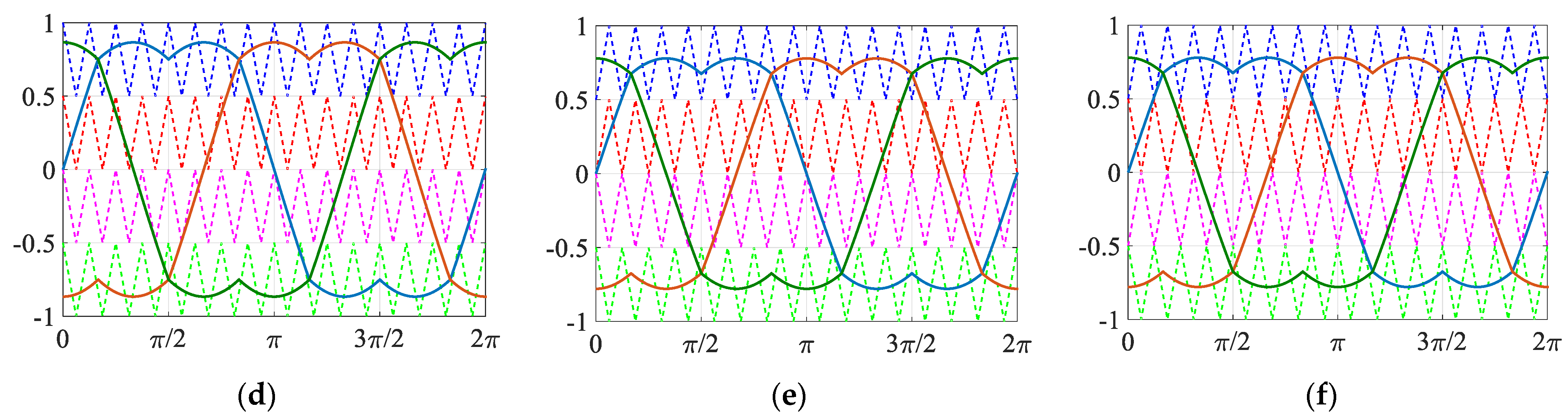
The PS-based and SCAMOD-based modulation schemes tested and considered in this work follow:
Sinusoidal Phase Shifted—SPS (
Figure 6a);
Sinusoidal Suppressed Carried Arrangement Modulation—SCAMOD (
Figure 6b);
Switching Frequency Optimal Alternative Phase Shifted—SFOPS (
Figure 6c);
Switching Frequency Optimal Suppressed Carried Arrangement Modulation—SFOSCAMOD (
Figure 6d).
In the next section, a brief discussion regarding implementation issues and improvements to obtain high performance with minimal hardware resources is presented.
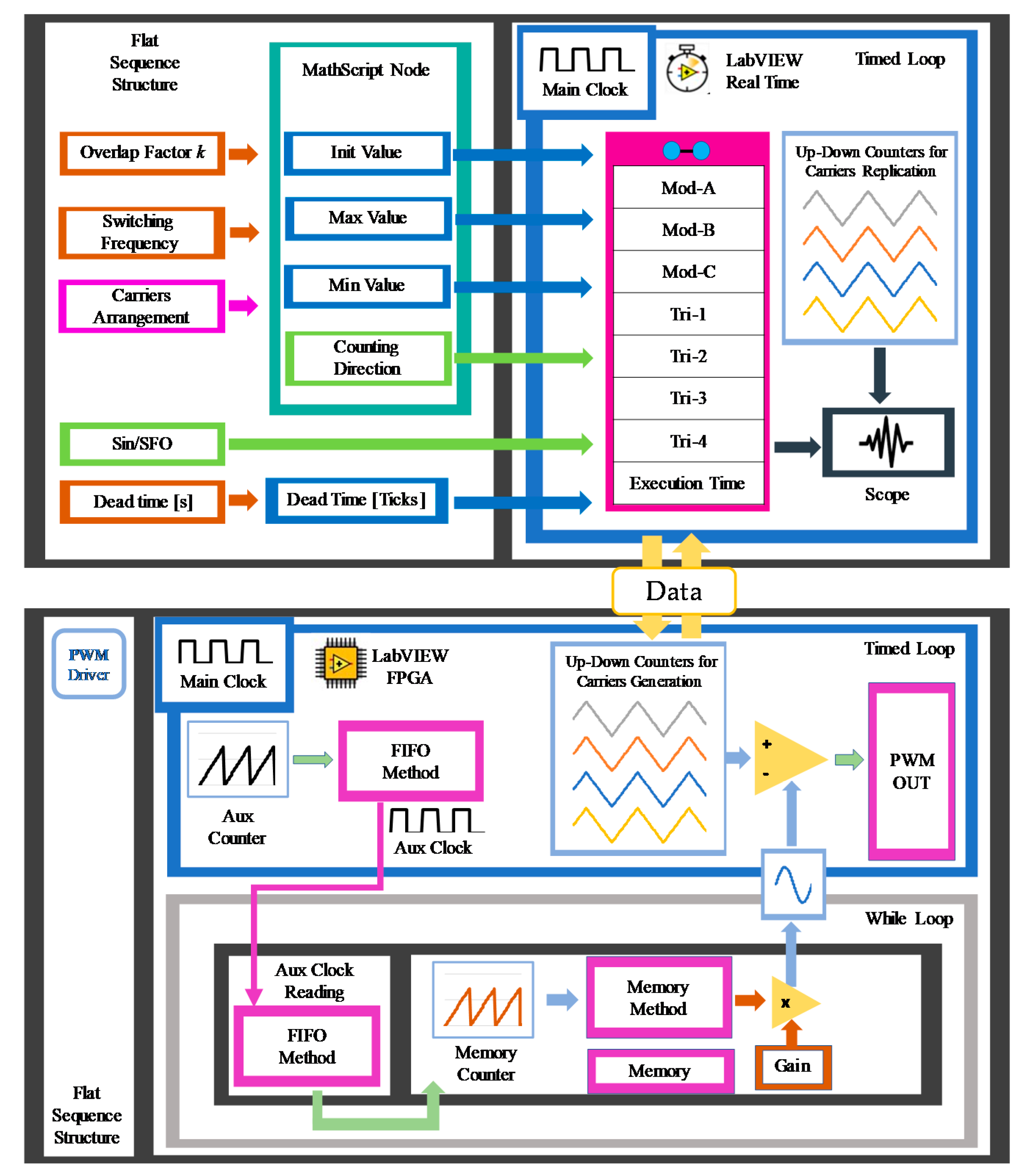
3. Control Software Design and MC PWM Implementation
All the techniques described in the previous section were implemented on a sbRIO 9651 System on Module (SOM). The controller consists of two different units: an ARM Cortex-A9 processor, used for real-time process management, and an Artix-7 FPGA unit, used for high-frequency control. Both units can be programmed individually, choosing the desired target in the LabVIEW project [
39]. Furthermore, the sbRIO 9651 SOM is equipped with some peripherals that allow an easy and user-friendly approach to the realization of Power Electronics and Drive applications (PED) control. Commercially, this system is called a PED-board. The PED-board main features are summarized in
Table 1.
To highlight the improvement brought to the new implementation of the control approach with respect to that carried out in the previous work [
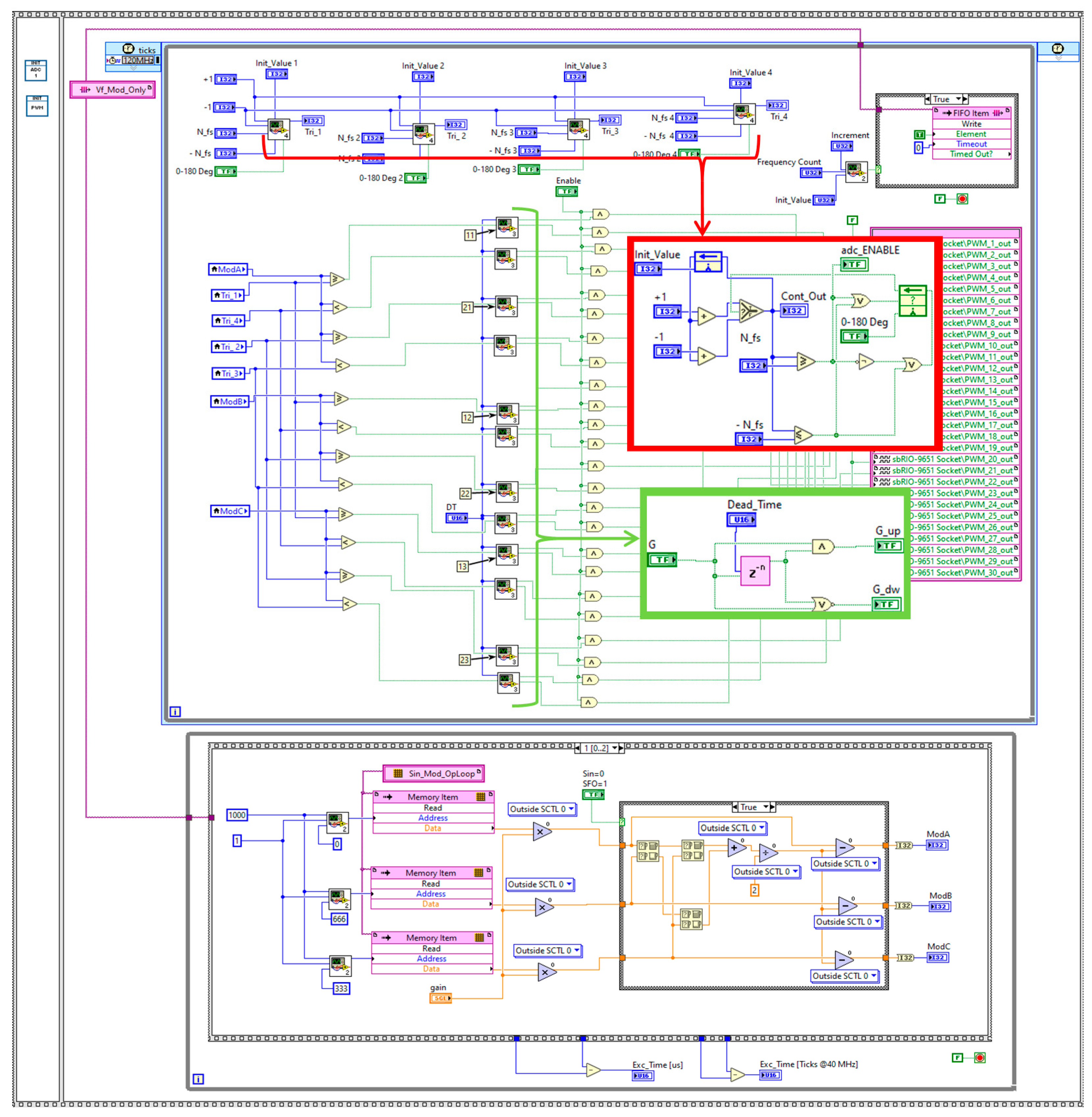
40], the last one here is briefly summarized. In the FPGA target, a Flat Sequence Structure (FSS) with two frames is placed. In the first frame, the initialization of PWM I/O nodes is implemented, placing in there the PWM I/O Driver. The second frame contains the control itself; in particular, two structures are placed there: a Timed Loop (TL) and a While Loop (WL).
Into the TL, the generation of carrier signals is carried out by four up–down counters; the arrangement of the carriers can be set by the user, acting on the counter parameters, i.e., the initial value of counting, maximum value, minimum value, and counting direction. PWM signal generation is carried out by the comparison of carriers and modulating signals by relational operators. In TL, a reset counter is also placed that generates an Aux Clock and, subsequently, the operations in WL are enabled. TL operations are executed at a 120 MHz clock, while operations in WL are executed at a clock frequency that is a function of desired modulating signal frequency. The generation of the modulating signals is realized in the WL. In particular, three reset counters (one for each phase) are used to extract elements by a pre-allocated vector of 1000 elements, representing one sinewave signal period. Subsequently, the sinewave amplitude is matched with the carriers’ amplitude and, if required, SFO modulating signals are generated.
In [
40], the entire control algorithm has been implemented on the FPGA target only, including all operations related to the carrier’s parameter calculation, for fixed control strategy and the carrier’s frequency. This kind of operation is implemented as single precision floating point data; thus, on one hand, a high computational cost is required, on the other hand, this kind of operation could be performed with a very low clock frequency or, at the most, only once. Based on these considerations, all operations for the aux parameter calculation were moved from the FPGA target to the Real-Time Target (RTT). Therefore, the FPGA target contains only the control main structure, and it is completed by the complementary operations executed in RTT. In particular, in RTT, another two-frame FSS is placed. The first frame contains all operations to be executed only once, i.e., dead-time conversion from seconds to clock ticks and the carrier’s parameter calculations. To realize parameter calculation, the MathScript Node is used: it allows for implementing operations with a textual language instead of linking blocks. Parameter calculation is generalized; for each carrier arrangement, introducing an Overlap Factor
k, owing to the Carrier Overlap PWM (CO-PWM), can be realized. In this work,
k is constantly set to 0; thus, no carrier overlap is realized.
The second frame contains the timed loop that addresses the signals exchanged with the FPGA target and the signal monitoring. The LabVIEW FPGA and real-time block diagrams are synthesized in
Figure 7.
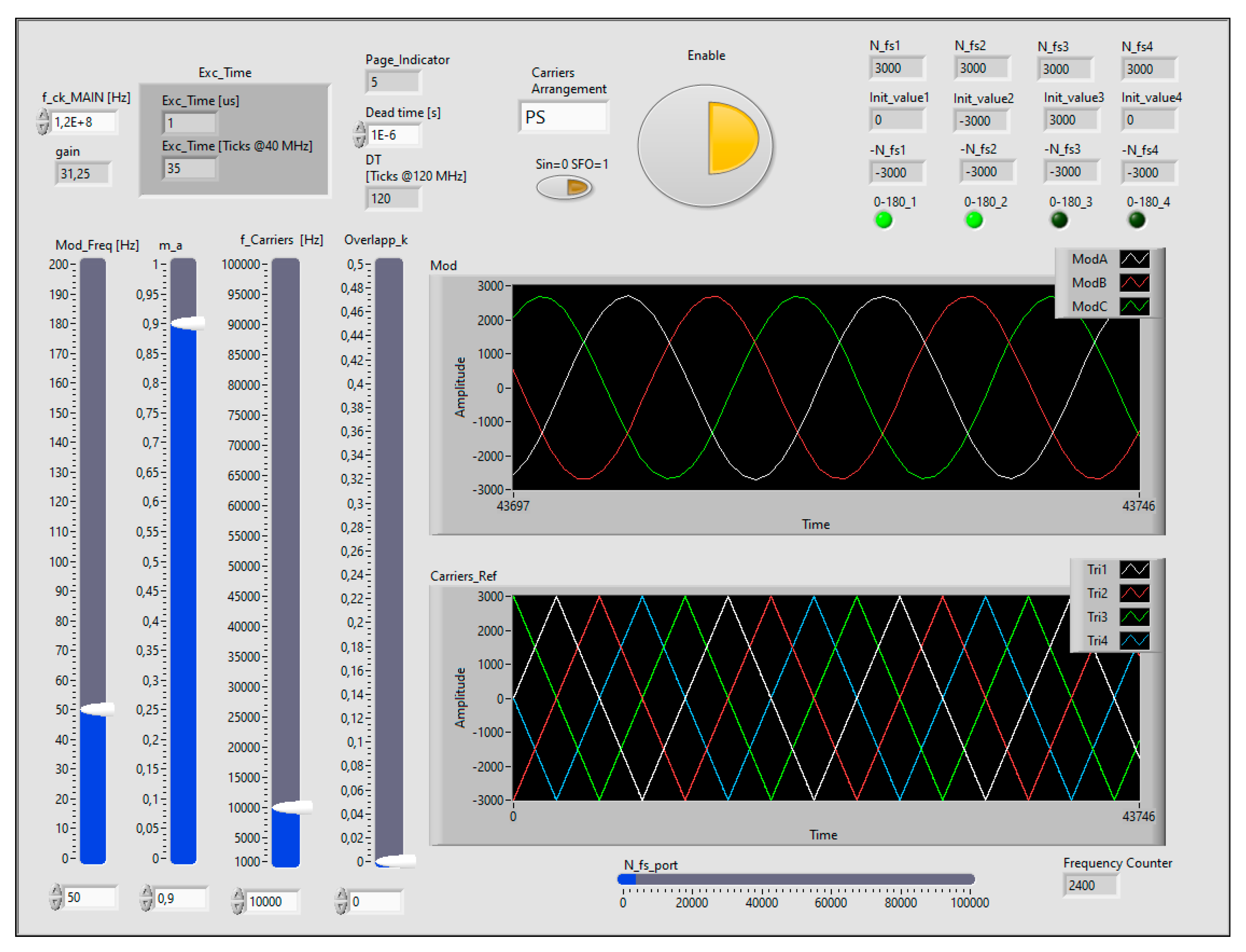
The user interface is developed in the real-time target front panel and is shown in
Figure 8. There, carrier signals, modulating signals, and relative parameters can be monitored; modulation index amplitude
ma, switching frequency
fsw, and modulating signals frequency
f, can be set by the user, owing to the relative sliders; desired carriers arrangement can be set, introducing in the text box the relative symbol (PD, POD, APOD, SCA, PS). The enable button allows for setting the PWM outputs to zero value.
Owing to the RT and FPGA target coordination, the control algorithm computational cost is drastically reduced.
Table 2 reports the computational cost comparison obtained with the control algorithm implementation on the FPGA target [
40] and the proposed control algorithm implementation on FPGA and real-time targets. It can be noted that the number of total slices in percentage used is reduced from 88.5% to 38.2%; thus, a drastic reduction of FPGA resources is obtained.
Concerning the control complexity, once the main structure operating principles are known, the control realization is extremely easy; in detail, an interesting way to simplify the programming workflow is to create Sub-VI-containing structures that are often repeated along with the code, such as the up–down counters for generation of the carriers and the dead-time generators. By way of an example, in
Figure 9, the front panel in FPGA target is presented: the structure of the up–down counter is presented in the red square, while the dead-time generation structure is in the green square.
This programming approach is modular, so that all of the LabVIEW structures and SubVIs can be reused to implement the control of any kind of inverter.
It is interesting to make a comparison between the three-phase five-level CHBMI (3P5L CHBMI) and traditional Three-Phase Two-Level Inverter (3P2L Inverter) control complexity. The difference between the two control programs lies in the number of up–down counters and dead-time generators required: in the 3P5L CHBMI four counters and twelve dead-time generators are required, while in the 3P2L Inverter one counter and three dead-time generators are required. Regardless, since both these structures are implemented using Boolean or long-int 32-bits signals, the number of structures used does not drastically change the required control computational cost.
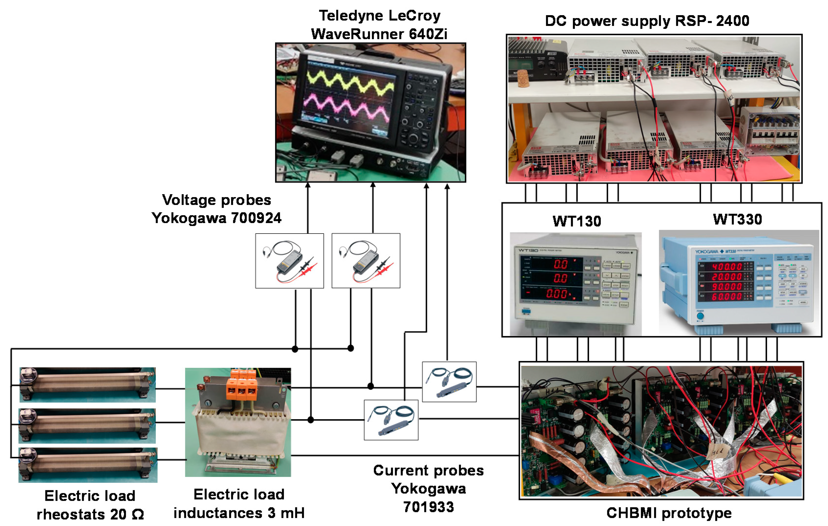
5. Experimental Results and Discussions
This section is devoted to the presentation of the experimental results obtained in this work by using all modulation schemes discussed in
Section 2. This work aims to evaluate the switching frequency effects in the harmonic distortion of the output voltages and the conversion efficiency. In detail, the experimental tests are conducted by supplying the RL load for different values of the AC output power, by changing the modulation index, and for different values of the switching frequency.
Table 5 summarizes the main electric quantities of the converter system and highlights the switching frequency and modulation index variation ranges.
In detail, seven different switching frequency values from 10 to 70 kHz, with a step of 10 kHz, and four different index modulation values equal to 0.3, 0.6, 0.1, and 1.15 are considered in the experimental investigations.
As described in
Section 4, the DC and AC electrical quantities are acquired and subsequently elaborated to evaluate voltage THD% and conversion efficiency.
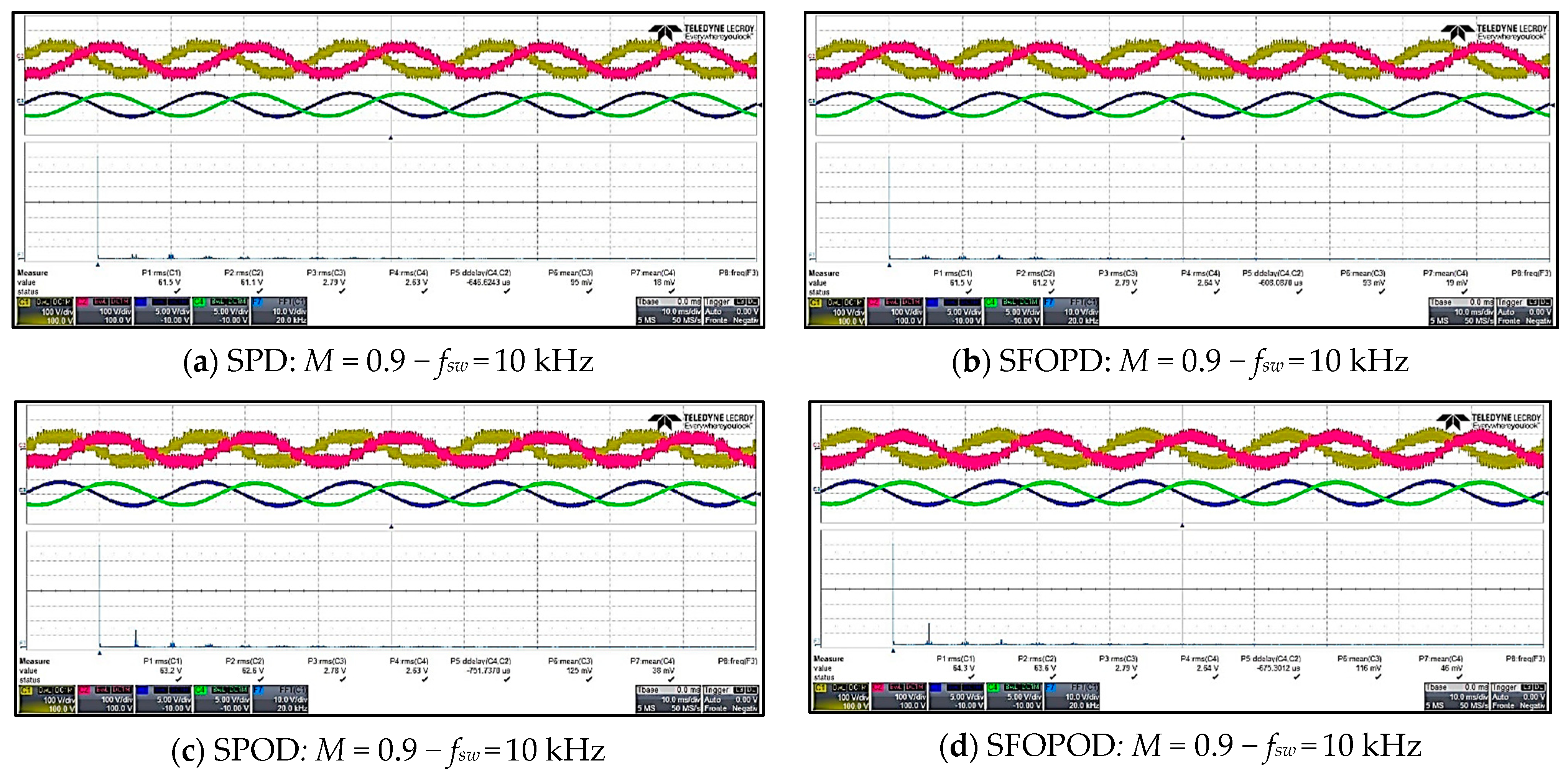
Figure 12 and
Figure 13 show, for each modulation schemes taken into account in this work, the phase voltages (yellow and red curves in the first grid), line currents (blue and green curves in the first grid), and corresponding voltage harmonic distribution in the frequency domain (blue bar graph in the second grid) for phase A and B of the system, respectively. In detail, in
Figure 12 the acquisitions are carried out for a modulation index equal to 0.9 and a switching frequency equal to 10 kHz. Moreover, the voltage scale is set to 100 V/div and 10 ms/div, the current scale is set to 5 A/div, and the harmonic spectra in the frequency domain is set to 10 V/div and 20 kHz/div.
It should be noted that for the CD-based schemes, shown in
Figure 12a–f, the first harmonics are centered at the switching frequency, equal to 10 kHz in this case, and the more significant harmonics are up to four times the switching frequency equal to 50 kHz.
The PS-based schemes, shown in
Figure 12g,h, present a harmonic spectrum in which the first harmonics are centered at four times the switching frequency, equal to 40 kHz in this case, and the more significative harmonics are up to sixteen times the switching frequency equal to 160 kHz. Instead, the SCAMOD-based schemes, shown in
Figure 12i,j, present an intermediate behavior between CD-based and PS-based schemes. In particular, the first harmonics are centered at two times the switching frequency, equal to 20 kHz in this case, and more significative harmonics are up to eight times the switching frequency equal to 80 kHz.
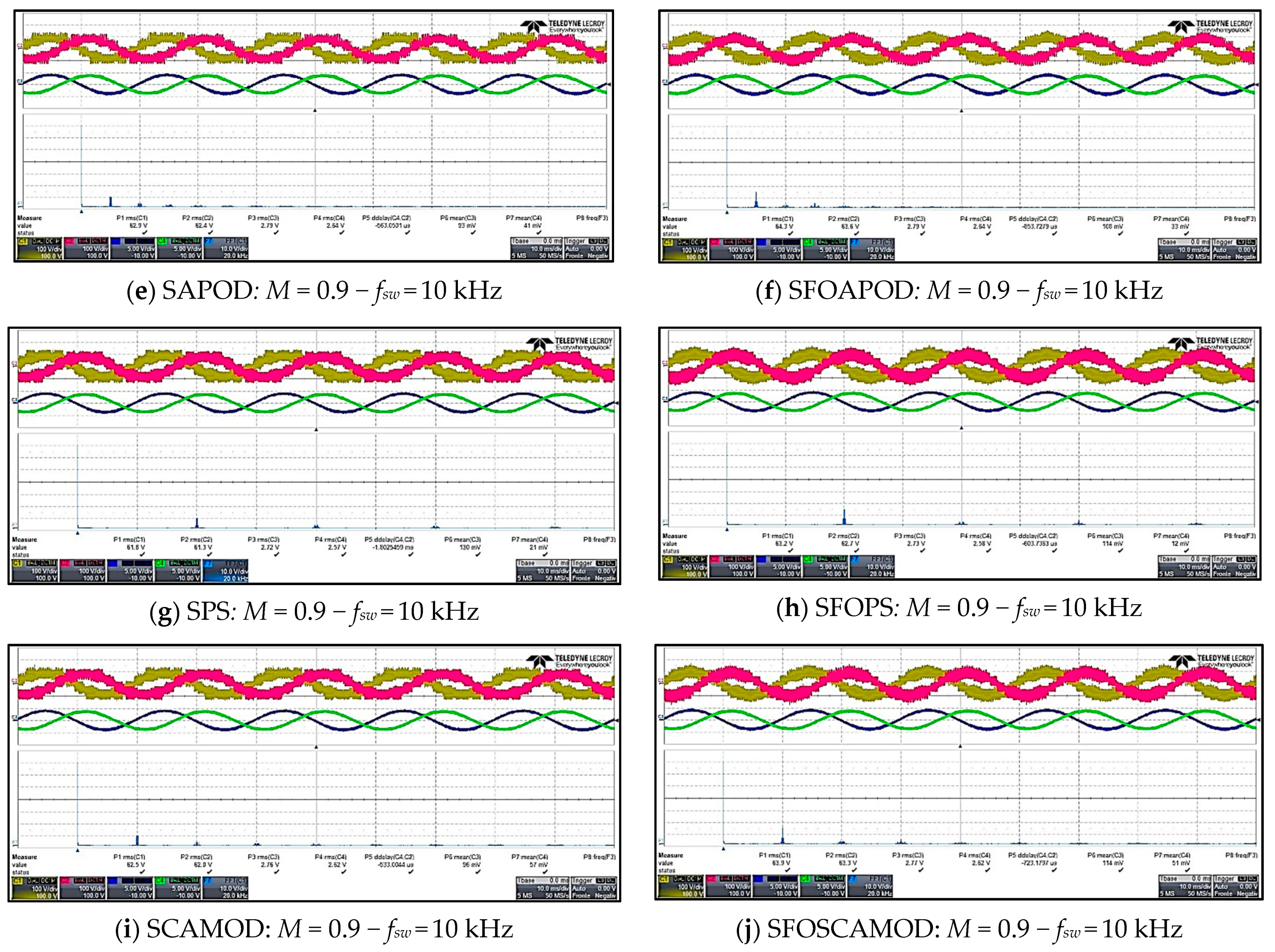
Figure 13 shows the same electric quantities of
Figure 12 with the same settings but for a switching frequency equal to 40 kHz. By analyzing
Figure 13, it is possible to observe that the same phenomena, previously described, is also observed in this case. Thus, these results confirm that each modulation scheme presents the same response in terms of the harmonics distribution in the frequency domain for different values of the switching frequency. Moreover, it is possible to demonstrate the effectiveness of the control algorithm implemented, as described in
Section 3.
In addition, the knowledge of the exactly harmonics distribution in the frequency domain and their entity toward high-frequency spectra allows for accurately designing the filter system.
The harmonic distortion analysis and the evaluation of the conversion efficiency are reported in the following two subsections.
5.1. Harmonic Distortion Analysis
To investigate the performance of the converter in terms of the harmonic distortion, the Total Harmonic Distortion (THD%) index [
4] is used as comparing tool and expressed in percent as
where
Vh is the generic voltage harmonic and
V1 is the fundamental voltage harmonic. As described in
Section 4, by using a sampling frequency equal to 10 MS/s in the THD% evaluation, the harmonics up to 5 MHz are considered, according to the Shannon theory.
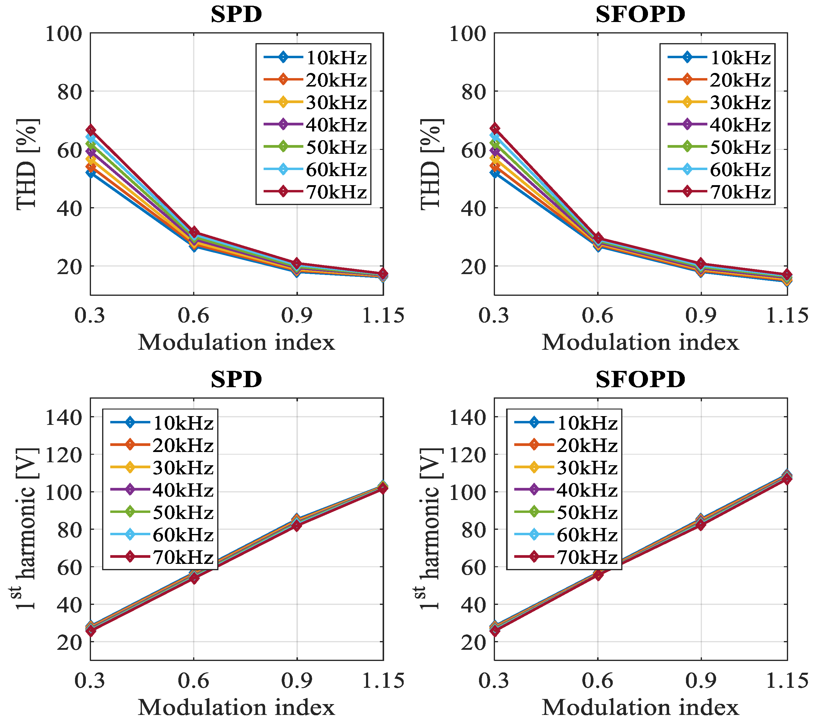
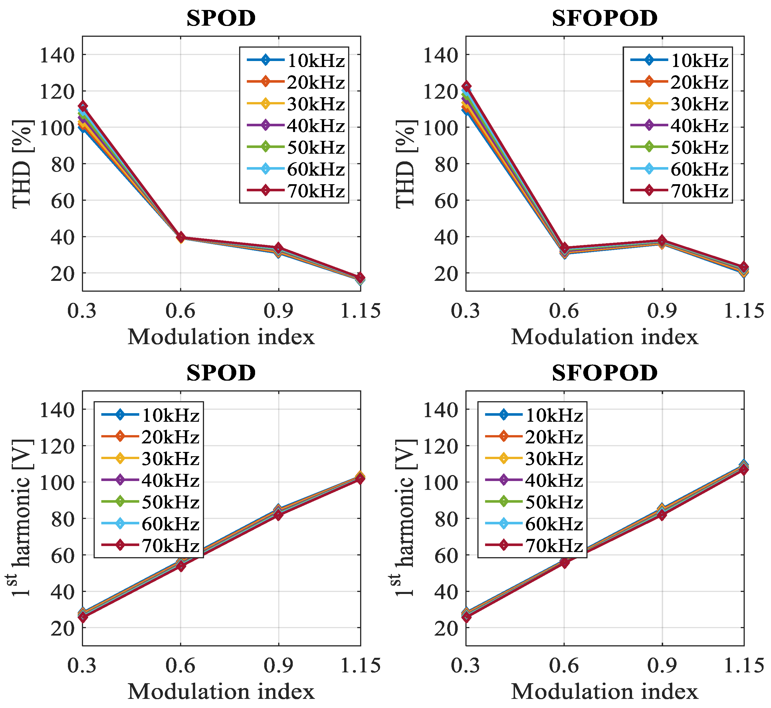
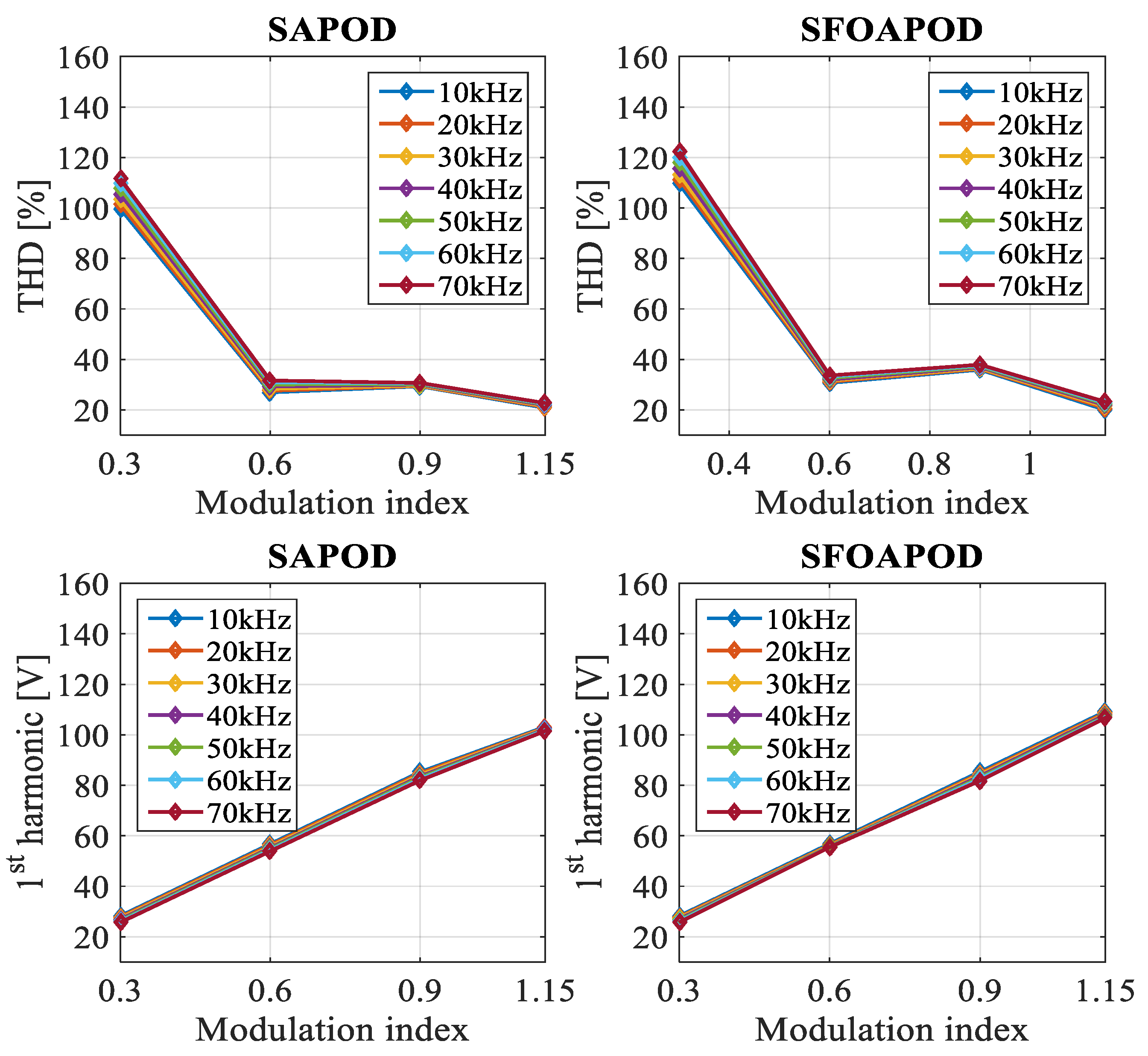
Figure 14,
Figure 15 and
Figure 16 show the THD% and first voltage harmonic trends as a function of the modulation index and for switching frequency from 10 to 70 kHz, obtained with CD-based schemes (PD, POD, and APOD) with sinusoidal and SFO modulation signals.
It is interesting to observe that the switching frequency effects are more evident for lower values of the modulation index, which generates a low increase of the THD%. Moreover, the fundamental amplitude appreciable variations are not detected in the switching frequency variation. Thus, it is possible to claim that CR-based schemes do not provide harmonic distortion significant variations to the switching frequency variation.
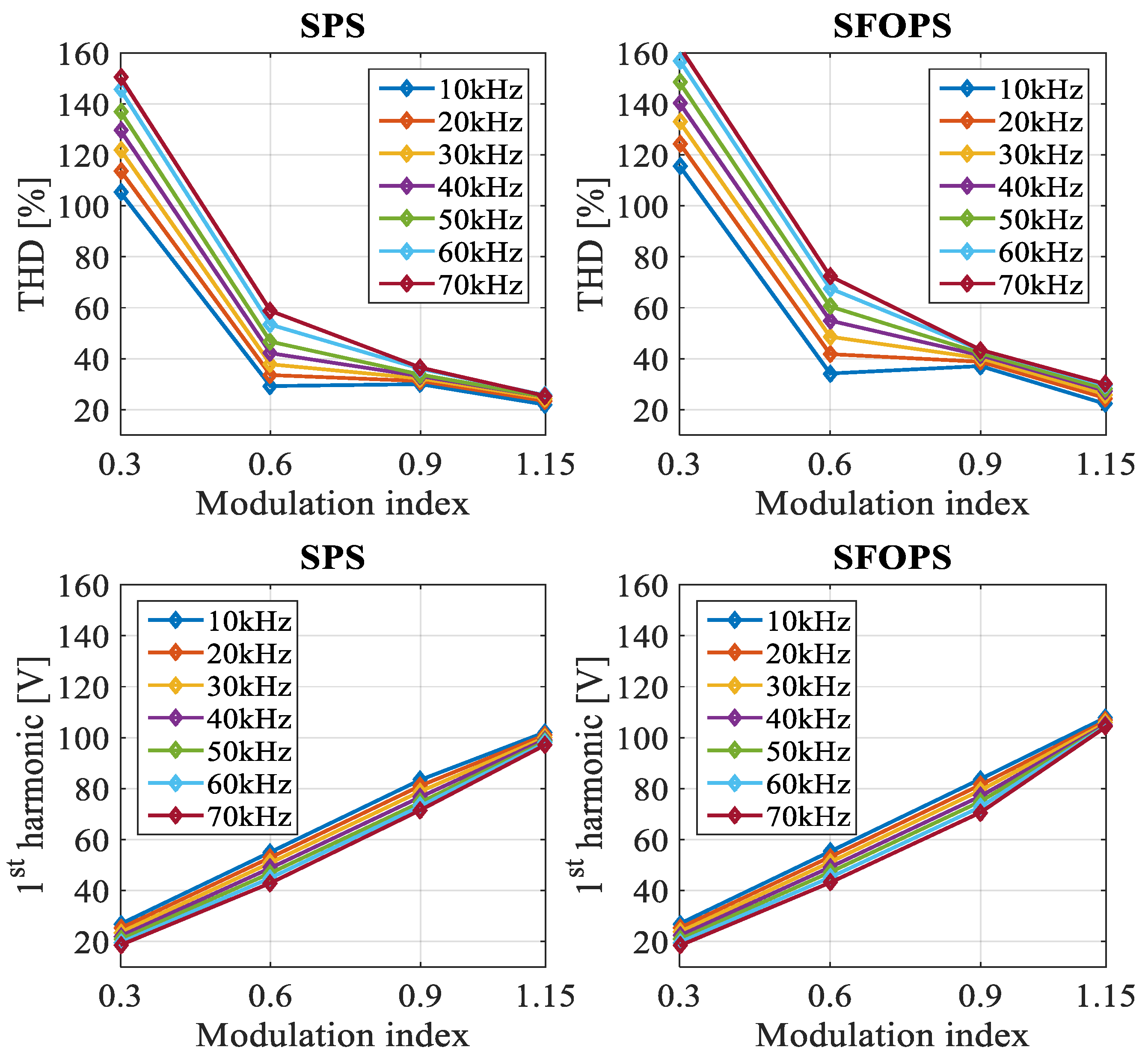
The THD% and first voltage harmonic trends obtained with PS-based schemes with sinusoidal and SFO modulation signals are illustrated in
Figure 17. In this case, an enhanced increase of the THD% trend and, in particular, for lower values of the modulation index, is observed. In detail, for a modulation index equal to 0.6, the THD% varies from about 28% at 10 kHz to approximately 60% at 70 kHz by using SPS modulation.
In the case of SFOPS, the THD% varies from about 34% at 10 kHz to approximately 77% at 70 kHz for the same value of the modulation index. For higher values of the modulation index, which correspond to higher values of AC output power, the switching frequency effects on the THD% values are significantly reduced.
By analyzing first voltage harmonic trends, for both SPS and SFOPS schemes a reduction of the voltage amplitude as the switching frequency increases is observed, which is more evident for lower values of the modulation index. By taking into account the expression (8), the reduction of the first voltage harmonic as the switching frequency increase explains the higher values of the THD%. The reduction of the first voltage harmonic is due to the high virtual switching frequency of the PS schemes and by the presence of the dead-time in the gate signals. In detail, by increasing the switching frequency, the time-width of the gate signals is reduced and becomes similar to the dead-time. Thus, this phenomenon generates the cancellation of some gate signals and the increasing overall distortion with respect to the ideal gate signals without dead-time.
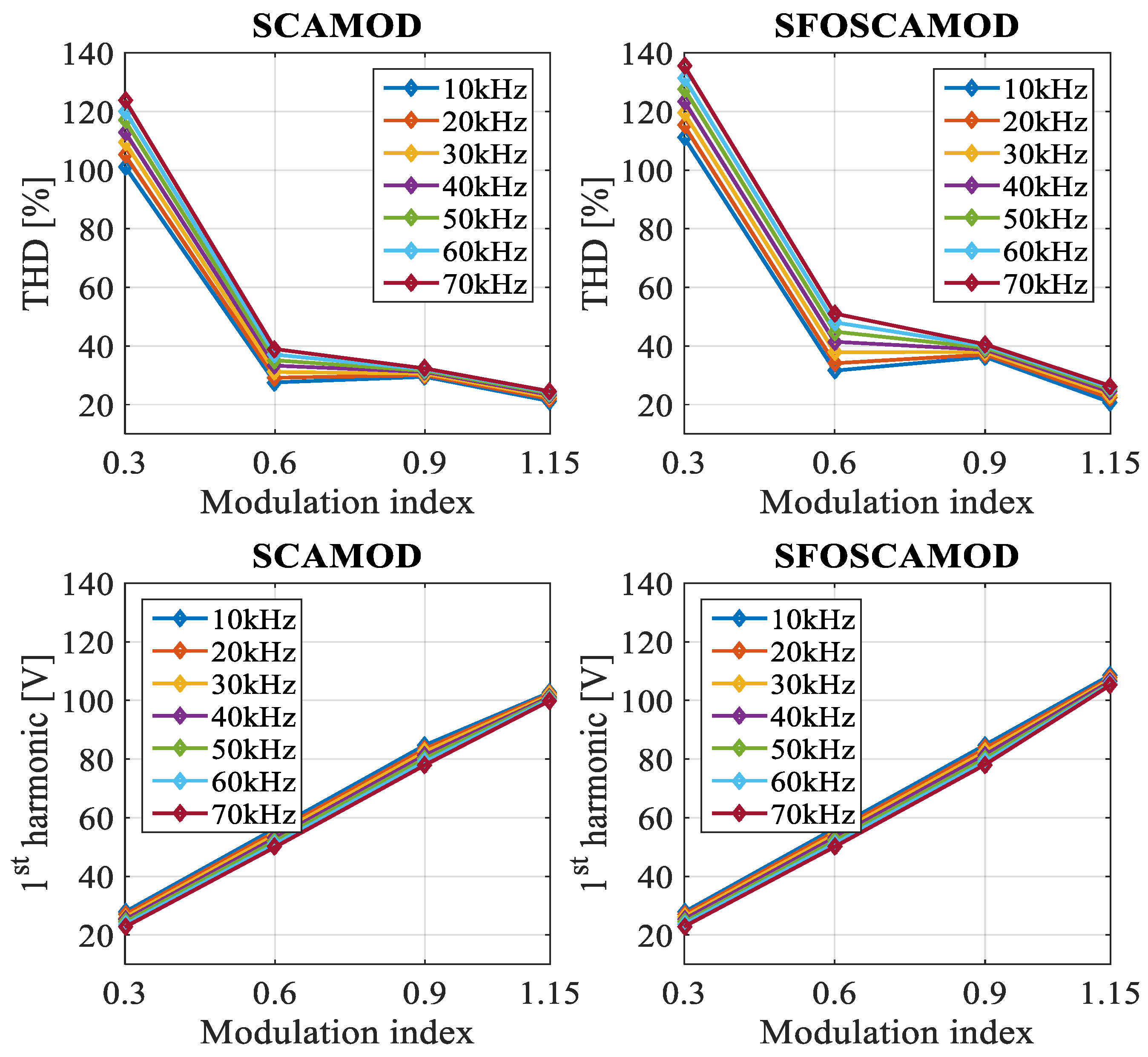
Figure 18 shows the THD% and first voltage harmonic trends as a function of the modulation index and for switching frequency ranging from 10 to 70 kHz, obtained with SCAMOD-based schemes with sinusoidal and SFO modulation signals, respectively. In this case, a lower increase of the THD% values and a lower decrease of the first voltage harmonic values emerge as the switching frequency increases with respect to the SPS and SFOPS schemes. It should be noted that SCAMOD-based schemes are affected by the same phenomenon as the PS-based schemes but in a more contained way.
Another interesting consideration concerns the comparison between sinusoidal and SFO schemes as modulation signals with the same carrier pattern. In particular, it is observed that the sinusoidal-based schemes present lower values of the THD% in all cases examined.
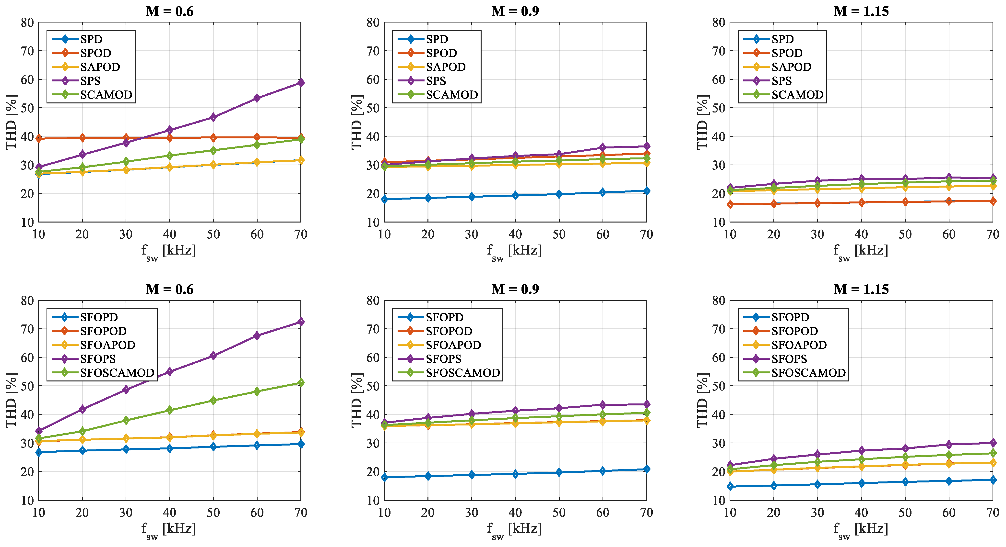
Figure 19 shows the switching frequency effects on the THD% among MC PWM schemes under test as a function of the switching frequency and for fixed modulation index. In detail, it is interesting to observe the THD% trends in the case of modulation index equal to 0.6, where the converter works with five voltage levels. The PS-based schemes show a significant increase of the THD% values as the switching frequency increases and a similar phenomenon can be observed with SCAMOD-based schemes. Instead, CD-based schemes show a constant trend as the switching frequency increases and lower values are obtained with the SFOPD scheme. For higher values of the modulation index, all THD% values present a constant trend as the switching frequency increases among the schemes considered.
To complete the voltage waveforms harmonic analysis, in
Table 6 some waveform features are summarized; in detail, the number of phase voltage and line-to-line voltage levels, the amplitude of the phase voltage, and the harmonic order with the maximum harmonic amplitude are presented. It is interesting to note that these features depend on the modulation scheme and modulating signals chosen, but they are not affected by the switching frequency, while the amplitude of each harmonic can depend on the switching frequency.
5.2. Conversion Efficiency Analysis
The second quantity analyzed and used for converter performance comparison purpose is the conversion efficiency
η expressed in percent as:
where
PAC is the AC output power,
PDC,i is the
ith DC input power of the corresponding H-bridge, and
nHB is the H-bridge overall number of the converter.
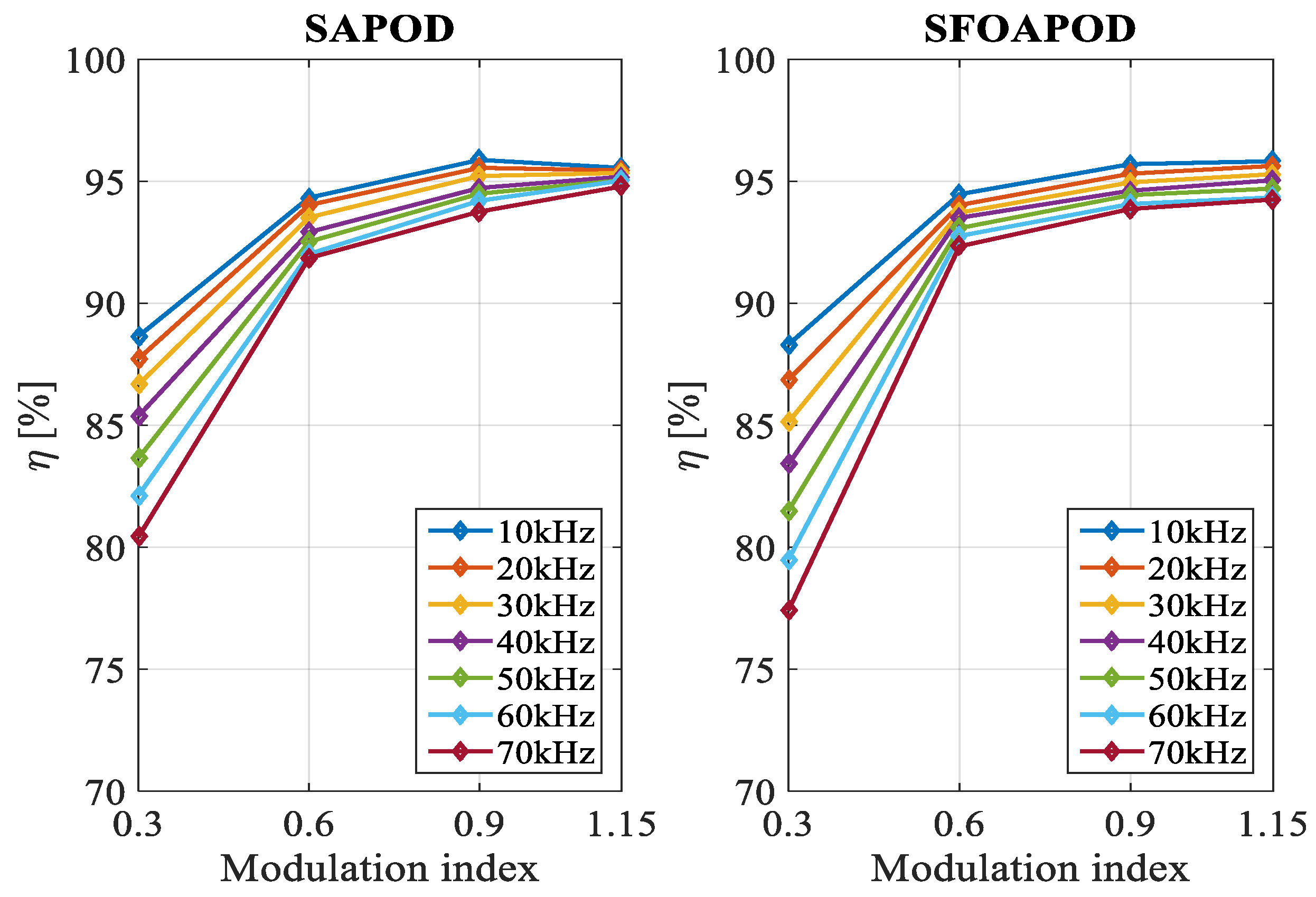
Figure 20,
Figure 21 and
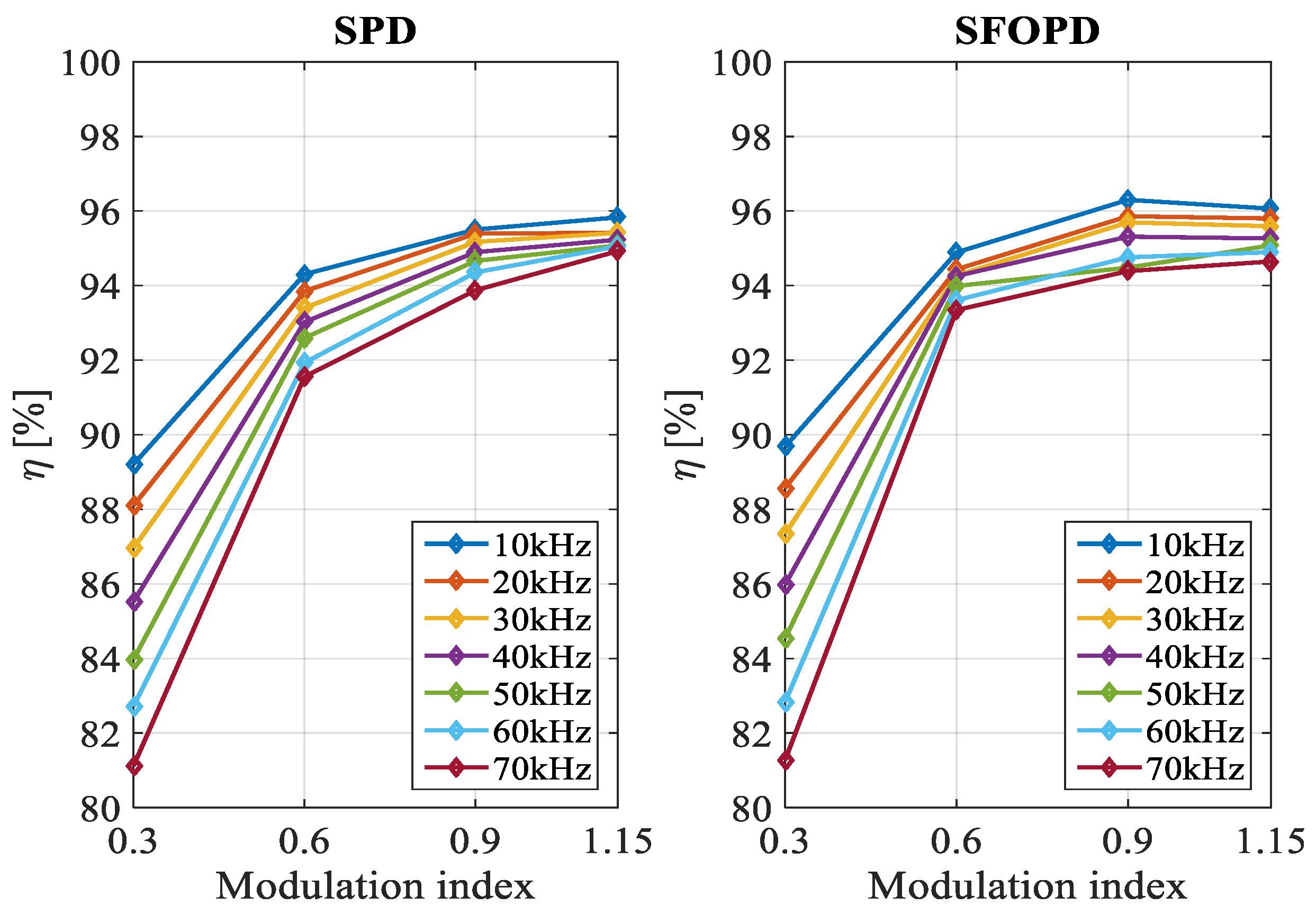
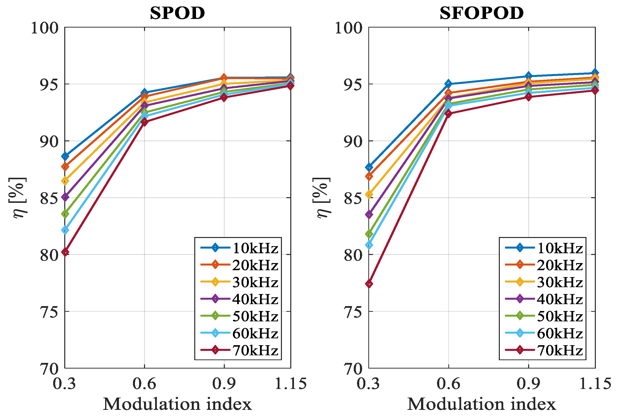
Figure 22 show the conversion efficiency trends as a function of the modulation index and for switching frequency values from 10 to 70 kHz, obtained with CD-based schemes (PD, POD, and APOD) with sinusoidal and SFO modulation signals, respectively.
As shown in
Figure 20,
Figure 21 and
Figure 22, the increase of the switching frequency generates a reduction of the conversion efficiency, which is further reduced as the modulation index decreases. This phenomenon is mainly due to the increase of the commutations number that generates an increase of the switching losses. Indeed, for higher values of the modulation index, which correspond to higher values of the AC output power, the conduction losses are predominant, and, for this reason, switching frequency effects on the conversion efficiency are reduced.
Another interesting consideration concerns the impact of the modulation signals in the scheme. In detail, by using SFO as modulation signals an increase of the efficiency for lower values of the switching frequency, is observed in all cases of the CD-based schemes.
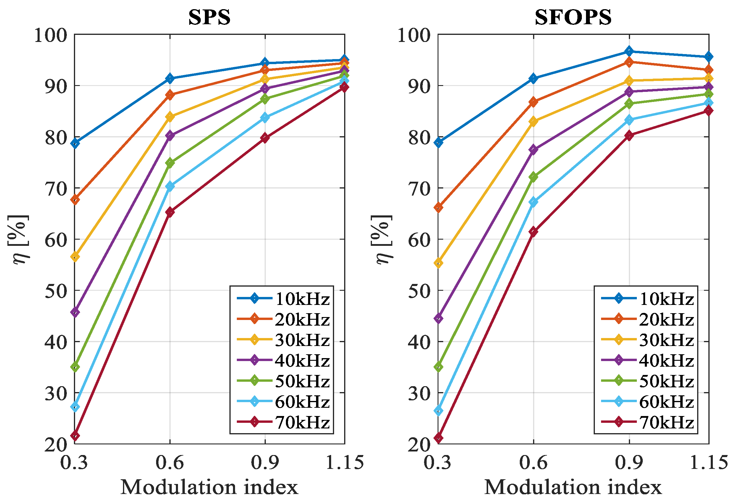
Figure 23 shows the conversion efficiency trends as a function of the modulation index and for switching frequency values from 10 to 70 kHz, obtained with a PS-based scheme with sinusoidal and SFO modulation signals, respectively.
In the case of the PS-based scheme, the switching frequency effects are highlighted to the CD-base schemes. Moreover, for lower values of the modulation index, the reduction of the converter efficiency is about 25%. Regardless, the same behavior emerges for the CD-based schemes for higher values of the modulation index. Moreover, also, in this case, the use of the SFO as modulation signals allows for increasing the efficiency values for lower values of the switching frequency.
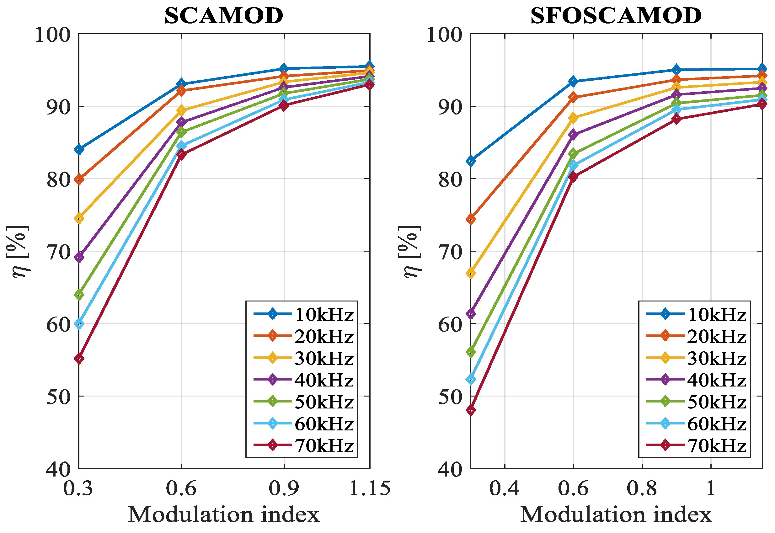
In the last case studied, SCAMOD-based schemes and the corresponding efficiency trends as a function of the modulation index and for different values of the switching frequency are shown in
Figure 24.
Additionally, the efficiency trends of the SCAMOD-based schemes are affected by the switching frequency effects. In detail, a reduction of the conversion efficiency has been observed as the switching frequency increases. Moreover, in the SCAMOD-based schemes, the SFO modulation signals do not generate any effects on the efficiency values.
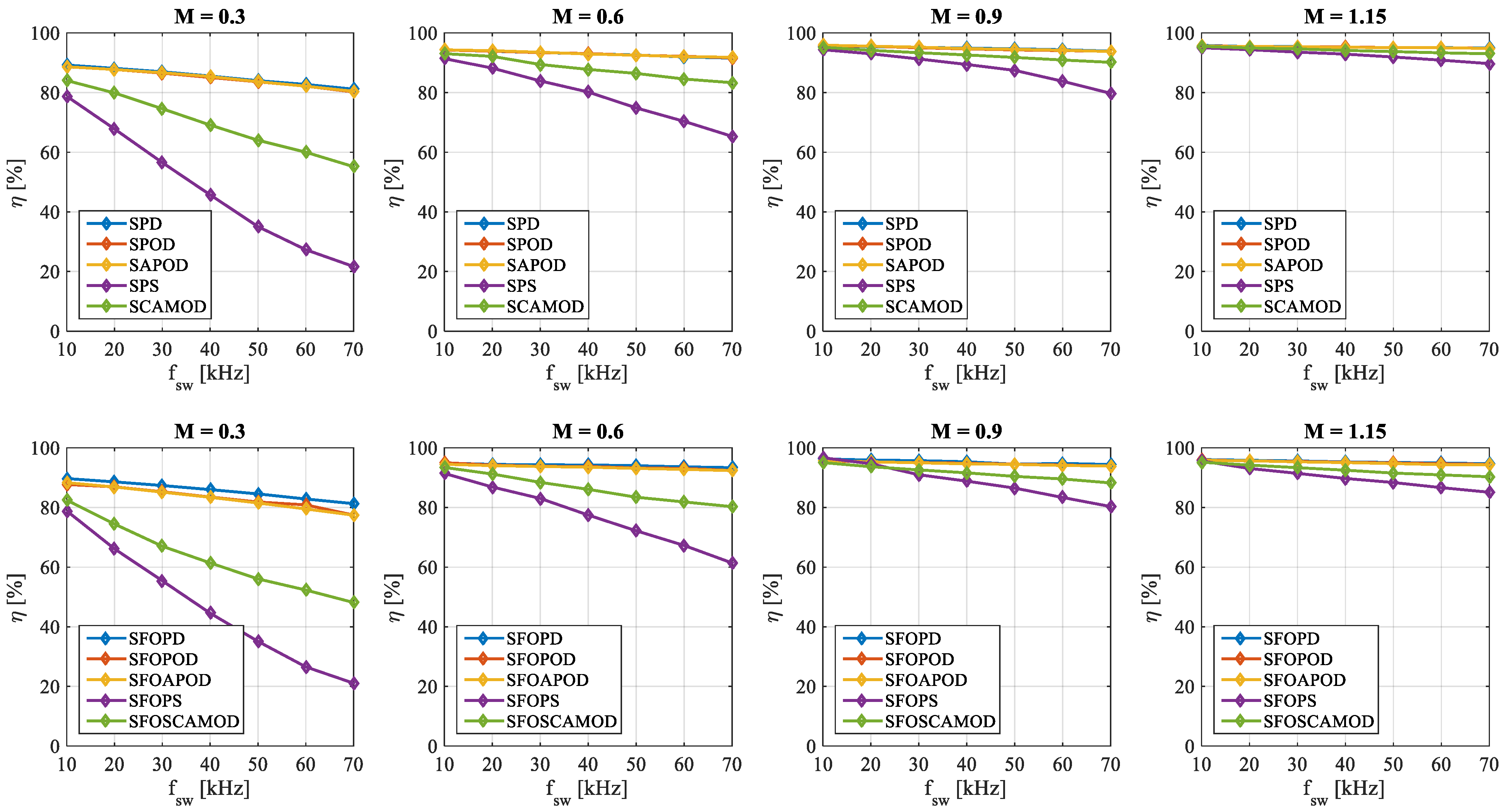
Figure 25 shows the comparison among modulation schemes with the same modulation signal as a function of the switching frequency and for different values of modulation index.
It is interesting to observe that through the analysis of
Figure 25 the switching frequency effects are more evident. In particular, for modulation index values less than 0.5, the converter works with three voltage levels. Thus, in these operating conditions, the worst efficiency results are obtained. Although all efficiency values present decreasing trends toward the high switching frequencies, CD-based schemes have higher values of efficiency and, in particular, the best results are obtained with the SFOPD scheme (blue curve).
For modulation index values over 0.5, the converter works with five voltage levels. Indeed, as shown in
Figure 25, the best efficiency results are obtained. The CD-based schemes present the same values of efficiency and, in detail, the best results for higher values of the switching frequency.
The worst efficiency results are obtained with PS-based schemes and, in particular, for higher values of the switching frequency. Regardless, it is necessary to observe that for switching frequency up to 30 kHz, efficiency values are comparable with the CD-based schemes. Moreover, it is necessary to consider that by using PS-based scheme voltage and current filtering are simpler with respect to the CD-based schemes with the same switching frequency.
The SCAMOD-based schemes present higher efficiency values with respect to the PS-based schemes. In detail, for higher values of the modulation index SCMAOD-based schemes present comparable efficiency values with the CD-based schemes. Regardless, the analysis carried out confirms that CHBMI performance obtained with the SCAMOD-based are intermediate between CD-based and PS-based schemes.
The case with a modulation index equal to 1.15 is very interesting. It should be noted that in this case higher values of the efficiency are obtained for all cases. Nevertheless, by using sinusoidal-based schemes in this condition, the converter works in the over-modulation region that, as well known, is an operating condition in transient time. By using SFO-based schemes, the converter works inside the linear-modulation region for modulation index values up to 1.15.


 ,
, 


