Reconfiguration of a Multilevel Inverter with Trapezoidal Pulse Width Modulation
by
 , , , and
Nataraj Prabaharan
1,* ,
,
V. Arun
2,
Padmanaban Sanjeevikumar
3,* ,
,
Lucian Mihet-Popa
4,* and
and
Frede Blaabjerg
5 1
School of Electrical and Electronics Engineering, Department of Electrical and Electronics Engineering, SASTRA Deemed University, Thanjavur 613401, Tamil Nadu, India
2
Department of Electrical and Electronics Engineering, Sri Vidyanikethan Engineering College, Tirupathi 517102, Andhra Pradesh, India
3
Department of Energy Technology, Aalborg University, 6700 Esbjerg, Denmark
4
Faculty of Engineering, Østfold University College, Kobberslagerstredet 5, 1671 Kråkeroy, Norway
5
Center of Reliable Power Electronics (CORPE), Department of Energy Technology, Aalborg University, Pontoppidanstræde 101, 9220 Aalborg, Denmark
*
Authors to whom correspondence should be addressed.
Energies 2018, 11(8), 2148; https://doi.org/10.3390/en11082148
Submission received: 16 July 2018
/
Revised: 10 August 2018
/
Accepted: 13 August 2018
/
Published: 17 August 2018
(This article belongs to the Special Issue Advanced Control Techniques for Power Converters)
Abstract
:This paper presents different multi-carrier unipolar trapezoidal pulse width modulation strategies for a reduced switch asymmetrical multilevel inverter. The different strategies are phase disposition, alternative phase opposition and disposition, and carrier overlapping and variable frequency that involve triangular waves as carriers with a unipolar trapezoidal wave as a reference. The reduced switch, asymmetrical multilevel inverter operation was examined for generating the seven-level output voltage using Matlab/Simulink 2009b and the results were verified with a real-time laboratory-based experimental setup using a field-programmable gate array. Different parameter analyses, such as total harmonic distortion, fundamental root mean square voltage, and distortion factor, were analyzed with different modulation indices to investigate the performance of the selected topology. Unipolar trapezoidal pulse width modulation provides a higher root mean square voltage value.
1. Introduction
The term multilevel originated from the two-level inverter. The elementary concept of the multilevel inverter (MLI) is used to achieve high power with several DC voltage sources. In an MLI, the amplitude of the output voltage is improved, which reduces the overall harmonic content and switching stress of the device [1,2]. Generally, the flying capacitor multilevel inverter (FCMLI), diode clamped multilevel inverter (DCMLI), and cascaded multilevel inverter (CHBMLI) are the three main topologies of the conventional multilevel inverter. The FCMLI is hard to comprehend because it contains many clamping capacitors and a DC bus capacitor. The DCMLI structure remains the same as the FCMLI, but clamping diodes are used instead of clamping capacitors. In addition, FCMLI and DCMLI are difficult to extend the level of the output voltage because of the use of the DC bus capacitor. The balancing of the DC bus capacitor is the major concern in both topologies [3,4]. The most popular conventional MLI is CHBMLI, which has many attractive features, such as a simple and modular design, requires fewer component counts, and averts a unbalance in capacitor voltage. The symmetric CHBMLI requires isolated DC sources with equal voltage whereas the asymmetric requires isolated DC sources with unequal voltage. The DC source ratios 1:2:4 and 1:3:9 are termed as binary and trinary, respectively [5].
Subsequently, several reduced switch MLI topologies have been addressed in symmetric, asymmetric, and hybrid conditions with pros and cons for the different applications. In [6], a stepped ladder-type cascaded inverter was presented. The presented ladder-type converter circuit consists on series connection of unit cells and it’s generated the maximum number of levels with fewer semiconductor devices, and supplied the sources and voltage on the switches. In [7], a lower switching frequency control pulse width modulation (PWM) technique was applied to MLI-fed AC drives. Lower switching frequency decreased the switching losses of the power semiconductor devices but increased the total harmonic distortion. In [8], a new topology for symmetric and asymmetric MLI was developed. An asymmetric MLI produced a high output voltage level compared to a symmetric MLI. A nine-level cascade neutral point clamped inverter with low switching frequency pulse width modulation (PWM) was presented in [9]. The capacitor voltage balancing was the major concern. Additional control techniques are required to maintain the capacitor voltage. A hybrid MLI based on a diode clamped type for both symmetrical and asymmetrical configurations was presented in [10]. However, the topology required more number of components. A different elementary division for CMLI was introduced in [11]. Each elementary division was connected in series, which produced only a positive level output voltage. An H-bridge was included with the elementary division to produce the output voltage in both positive and negative sequences. However, the basic unit required a greater component count. The harmonic investigation for a three-level NPCMLI-fed induction motor drive was investigated in [12]. In-phase sinusoidal PWM and phase opposition PWM were used to examine the system. The in-phase PWM method provided better results than the phase opposition. In addition, conventional PWM was used. An asymmetrical MLI for traction drives was discussed in [13]. A new hybrid inverter topology with common mode voltage elimination for an induction motor drive was presented in [14]. This topology has only one DC source and different voltage levels were generated using the floating capacitors. A reduced switch cascaded multilevel inverter with several transformers and a single DC source was discussed in [15]. A transformer on the secondary side was used to increase the output voltage level, but the cost and size of the transformer are very high. In [16], an effective structure of an MLI that increases the number of output voltage levels with a reduced number of circuit components was presented. This topology could not prefer a higher power application because it had the diodes with a combination of switches. A novel PWM modulating technique for a hybrid multilevel inverter was described in [17]. The carrier waveform originated from the phase disposition carrier arrangement. Novel carrier-based PWM in neutral-point (NP) balancing in the three-level inverter was presented in [18]. A hybrid modulation technique for cascaded MLI for high power applications in renewable energy systems was examined in [19]. A new dual port asymmetrical MLI with reduced conversion stages to improve the overall conversion efficiency of the system was discussed in [20]. The neutral point clamped type and T-type three-level cells were combined to build a dual port asymmetrical MLI. The developed topology provided better efficiency for various DC/AC power systems [21].
The conventional topology DCMLI requires 6 DC bus capacitors, 12 switches, and 24 clamping diodes while the FCMLI requires 6 DC bus capacitors, 12 switches, and 12 clamping capacitors to generate the seven-level output voltage. However, the selected reduced switch asymmetric multilevel inverter requires only eight switches to generate the same voltage. This paper focuses mainly on the different multi-carrier strategies with a unipolar trapezoidal reference. The different multi-carrier arrangements, such as phase disposition (PD), alternative phase opposition and disposition (APOD), carrier overlapping (CO), and variable frequency (VF) pulse width modulation strategies are involved for generating the seven-level output voltage. The carrier count of a unipolar method has been reduced by half compared to the conventional PWM method, which is the main advantage of this implementation. The reduced switch single-phase MLI was tested with the resistive and inductive (RL) load using the Matlab/Simulink (2009b). Experimental work was carried out using an FPGA system for strengthening the simulation results. The different parameters were evaluated and compared with each other at different modulation indices. The VFPWM method indicates a better performance compared to the other methods. In addition, the topology can be easily integrated with an appropriate solar-based converter by replacing the separate DC sources to achieve good performance in the photovoltaic application.
2. Single-Phase Seven-Level Reduced Switch Asymmetrical Inverter
Generally, the number of semiconductor device requirement for the MLI configurations depends on the number of output voltage level. However, increasing the number of power semiconductor devices leads to an increase in the topology design complexity, cost, and control difficulty. An asymmetric multilevel inverter (AMLI) can be utilized to achieve a higher number of output levels with the minimum number of power semiconductor devices compared to symmetric MLIs [8]. Feeding the converters with unequal DC voltages (asymmetrical feeding) increases the number of levels generated at the output voltage without any supplemental complexity to the existing symmetric topology.
Figure 1 shows the single-phase asymmetric seven-level inverter configuration. The selected asymmetric inverter consists of sub-multilevel inverters (low-power cell) and H-bridge (high-power cell) inverter. Sub-multilevel inverters are connected in series to achieve the desired number of voltage levels. Each sub-multilevel inverter has its own DC source and two power devices. The first sub-multilevel inverter consists of one DC source (VDC) and two switches designated as S1 and S2 whereas the switches S3 and S4 and voltage source (2VDC) are placed in the second sub-multilevel inverter. Both sub-multilevel inverters are connected in series and generate the required output voltage level at positive polarity. To operate as an inverter, it is necessary to change the voltage polarity in every half cycle. For this purpose, an H-bridge inverter is added with the sub-multilevel inverters. It is important to note that the switches of the H-bridge must withstand the higher voltage. This should be considered in the design of the inverter. However, these switches are turned ON or OFF only one time during a fundamental cycle. Therefore, these switches would be high-voltage and low-frequency switches. The zero output voltage is obtained when the switches S2 and S3 are turned ON, and simultaneously the other voltage levels are generated by the proper switching between the switches. Table 1 shows the switching table for generating each output voltage level. The generalized formulas for generating the output voltage level, maximum step output voltage, and the required number of devices and DC source are discussed below.
3. Modulation Strategies for Asymmetrical Multilevel Inverters
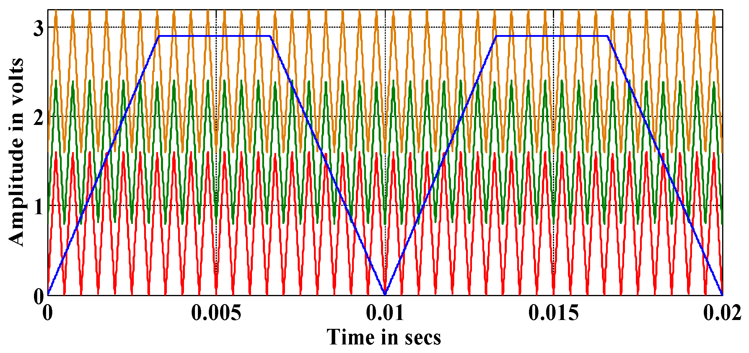
MLIs offer several advantages, but the control strategies are quite challenging due to the complexity of generating the voltage level transition (or steps) [21]. Many PWM strategies are used in MLIs for different applications [22]. The PWM techniques are usually employed in MLIs, which can be classified into three main categories: (1) multi-step, fundamental frequency or staircase switching strategies, (2) space vector PWM strategies, and (3) carrier-based PWM strategies [23]. The first category needs pre-calculated switching angles for generating the PWM signals [23]. The space vector method will be very complicated for more than five output voltage levels due to increases in switching states [24]. The carrier-based PWM methods are simple to use when the number of output levels is more than five [25,26]. Therefore, the carrier-based PWM method is preferred in this work. The carrier-based PWM is categorized into three groups: (i) carrier disposition methods where the reference signal is sampled through the number of carrier signals displaced by increments of the reference amplitude, (ii) phase shift PWM methods where the multiple carriers are phase shifted accordingly, and (iii) a combination of carrier disposition and phase shift methods. Control freedom degree (CFD) exists to design the carriers in multi-carrier PWM strategies [27]. These strategies have more than one carrier option, which can be triangular, sawtooth, and some new function, etc. The modulating wave can be a sinusoidal or an advanced reference signal. The CFD technique is used to determine the carrier type and its frequency, amplitude, the phase of each carrier, and the offset between carriers. The multi-carrier PWM strategies can also be categorized into two types: multi-carrier bipolar PWM (MCBPWM) strategies and multi-carrier unipolar PWM (MCUPWM) strategies. In this work, the unipolar MCPWM strategy is selected for making quality output voltage. In the unipolar strategy, the reference wave may be a rectified reference wave or two reference waves with a 180-degree phase shift. The multi-carrier is positioned above the zero level. For the unipolar multi-carrier technique, the M-level inverter requires (M-1)/2 carriers with the same frequency fc and same peak-to-peak amplitude Ac. The reference wave has the amplitude Am and frequency fm and it is placed at the zero reference. The different MCUPWM strategies, such as PDPWM, APODPWM, COPWM, and VFPWM, are utilized [8]. The carrier arrangement for the PDPWM strategy with unipolar trapezoidal reference is shown in Figure 2. The carriers of the same frequency and same peak-to-peak amplitude are placed so that the bands they occupy are contiguous [28,29]. The carrier set is placed above the zero reference [28]. In the APODPWM strategy, the carriers of the same amplitude and same frequency are arranged in such a manner that each carrier is out of phase with its neighbor by 180 degrees. Figure 3 shows the carrier arrangement for the APODPWM strategy [9]. The principle of COPWM is used to overlap the carriers with a single modulating signal. The carriers having the same frequency and same peak-to-peak amplitude are placed such that the bands they occupy overlap each other [8], as illustrated in Figure 4. In the VFPWM strategy, varying the carrier frequency based on the slope of the modulating wave in each band is represented in Figure 5. Positioned.
The main challenge is to reduce the switching losses of the inverter by reducing the switching frequency of the higher power cells. Therefore, instead of using MCUPWM (high-frequency carrier-based PWM) strategies in all the cells, the high-power cells are operated by a square waveform pattern switched at low frequency. Thus, the combination of MCUPWM (high frequency) and fundamental frequency (low frequency) switching modulation strategies was selected in this paper. In Figure 2, Figure 3, Figure 4 and Figure 5, it is noticed that the three triangular carriers and a unipolar trapezoidal reference are used to generate the switching pulses. The unipolar trapezoidal wave is continuously compared with triangular carriers and generates the Boolean outputs. The outputs of each carrier are represented by Pw1 to Pw3. By using the logical expression with Boolean outputs based on a switching table, the required PWM pulses are generated for the respective switches to generate the desired output levels. The logical expression for all switches is given in Equation (7). The switches A1 and A2 are triggered on when the reference wave is greater than or equal to zero and B1 and B2 are triggered on when the reference wave is less than or equal to zero. Figure 6 shows the graphical representation for generating the switching pulses to get the desired output.
4. Numerical Simulation Results
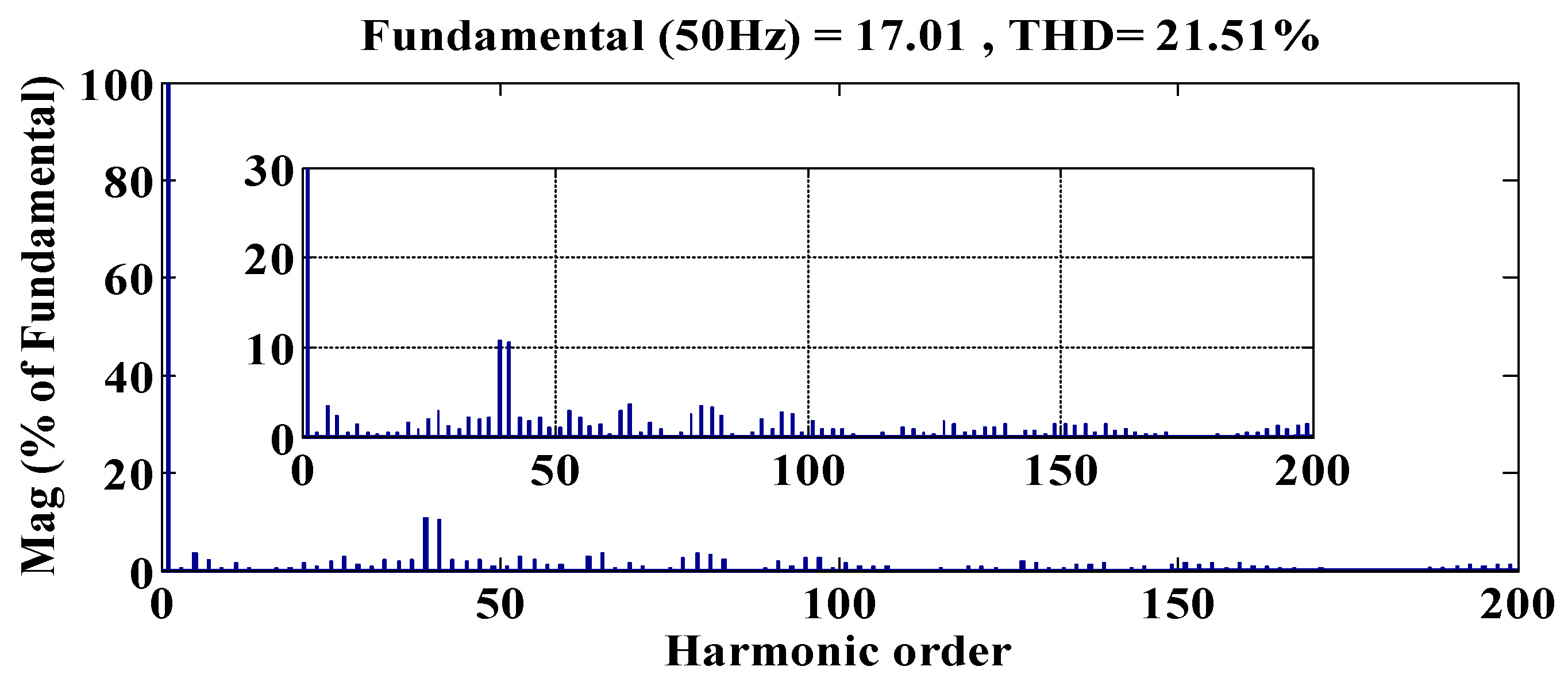
A single-phase reduced switch AMLI was modeled in Matlab/Simulink (2009a) to generate the seven-level output voltage by using a power system block set. Switching signals were developed using different multi-carrier unipolar PWM strategies as discussed in the previous section. Different parameters such as Vdc1 = 6 V, Vdc2 = 12 V, RL(load) = 100 Ω, 100 mH, fc = 2000 Hz, and fm = 50 Hz were utilized for simulation to evaluate the selected topology for the required output voltage. A simulation model was examined for different PWM strategies with various modulation indices ranging from 0.8–1. The % Total Harmonic Distortion (THD), fundamental root mean square (VRMS) values, and % distortion factor (DF) for the output voltage with various modulation indices were measured and tabulated. Here, all the results are displayed with different PWM strategies at the modulation index of 0.9. Figure 7a–b shows the seven-level output voltage waveform and the current waveform generated by the PDPWM strategy and its fast Fourier transform (FFT) plot is shown in Figure 8. The value of %THD is 21.51%. Figure 9a–b shows the seven-level output voltage waveform and the current waveform generated by the APODPWM strategy and its FFT plot is shown in Figure 10. The value of %THD is 21.03%. Figure 11a–b shows the seven-level output voltage waveform and the current waveform generated by the COPWM strategy and its FFT plot is shown in Figure 12. The value of %THD is 25.63%. Figure 13a–b shows the seven-level output voltage waveform and the current waveform generated by the VFPWM strategy and its FFT plot is shown in Figure 14. The value of %THD is 20.06%.
The %THD comparison of the output voltage for different PWM switching strategies with various modulation indices is shown in Table 2 and the corresponding graphical representation is shown in Figure 15a. The %THD depends on the range of switching frequencies. The frequency modulation index mf is defined as the ratio between the frequencies of the carrier fcr and modulating wave fm. When mf is a small number (i.e., less than 21), its output spectrum contains low-frequency harmonics (sub-harmonics) causing high currents in transformers and inductors. Note that in the case of mf being a large number, the amplitudes of the sub-harmonics are highly reduced and do not pose critical problems with the currents by inductors and transformers [6]. Therefore, the selected topology generates low order harmonics with the obtained high frequency, but the order harmonic values have considerable limits, i.e., within the IEEE 519 standard. Hence, low order harmonics do not affect the system. From Figure 15a and Table 2, it is observed that the harmonic content of the output voltage is lower for the VFPWM strategy than the other strategies. The RMS comparison of the output voltage for different PWM switching strategies with various modulation indices is shown in Table 3 and the corresponding graphical representation is shown in Figure 15b. From Table 3 and Figure 15b, it is observed that the CO strategy provides the highest DC bus utilization compared with the other strategies. The %DF comparison of the output voltage for different PWM switching strategies with various modulation indices is shown in Table 4 and the corresponding graphical representation is shown in Figure 15c. It is further visualized from Table 4 and Figure 15c that the VFPWM strategy has relatively lower harmonics after second order attenuation, indicated by the %DF. Figure 15d shows the harmonic content (amplitude values) for individual harmonic order. From Figure 15d, it is noted that the lower and upper sidebands (mf ± 1 and 2mf ± 1) appear in all strategies. In addition, the third-order harmonic is not dominant in all strategies. Harmonics corresponding to the center frequency mf, 2mf are minimum in all strategies. It is observed that the significant number of harmonics is avail by the VFPWM strategy using a trapezoidal reference carrier from the presented numerical results.
5. Implementation of Reduced Switch AMLI Using FPGA for Experimental Results
This section describes the experimental results for reduced switch asymmetric multilevel to examine seven-level output voltage using the SPARTAN-3 FPGA system. FPGA was used for real-time implementation, which usually includes an on-chip PWM controller to reduce the complexity of PWM signal generation. Multi-carrier PWM strategies with a unipolar trapezoidal reference were used for generating the PWM signal to the selected topology. The simulation part was implemented in Matlab/Simulink (2009a) ((PWM signal generation)) and converted into an input signal of FPGA through the Xilinx software (compiled and converted into bits and then downloaded into FPGA for execution in the real-time process). Figure 16 depicts the laboratory-based experimental setup for reduced switch AMLI. The experimental setup consists of power converter module MLI and gate terminals are trigger through FPGA digital processor and is programme through Xilinx software. The hardware parameters includes the voltage value of the DC sources Vdc1 = 6 V and Vdc2 = 12 V, the RL load values are 100 Ω, 100 mH, and the switching carrier frequency (fc) as 2000 Hz.
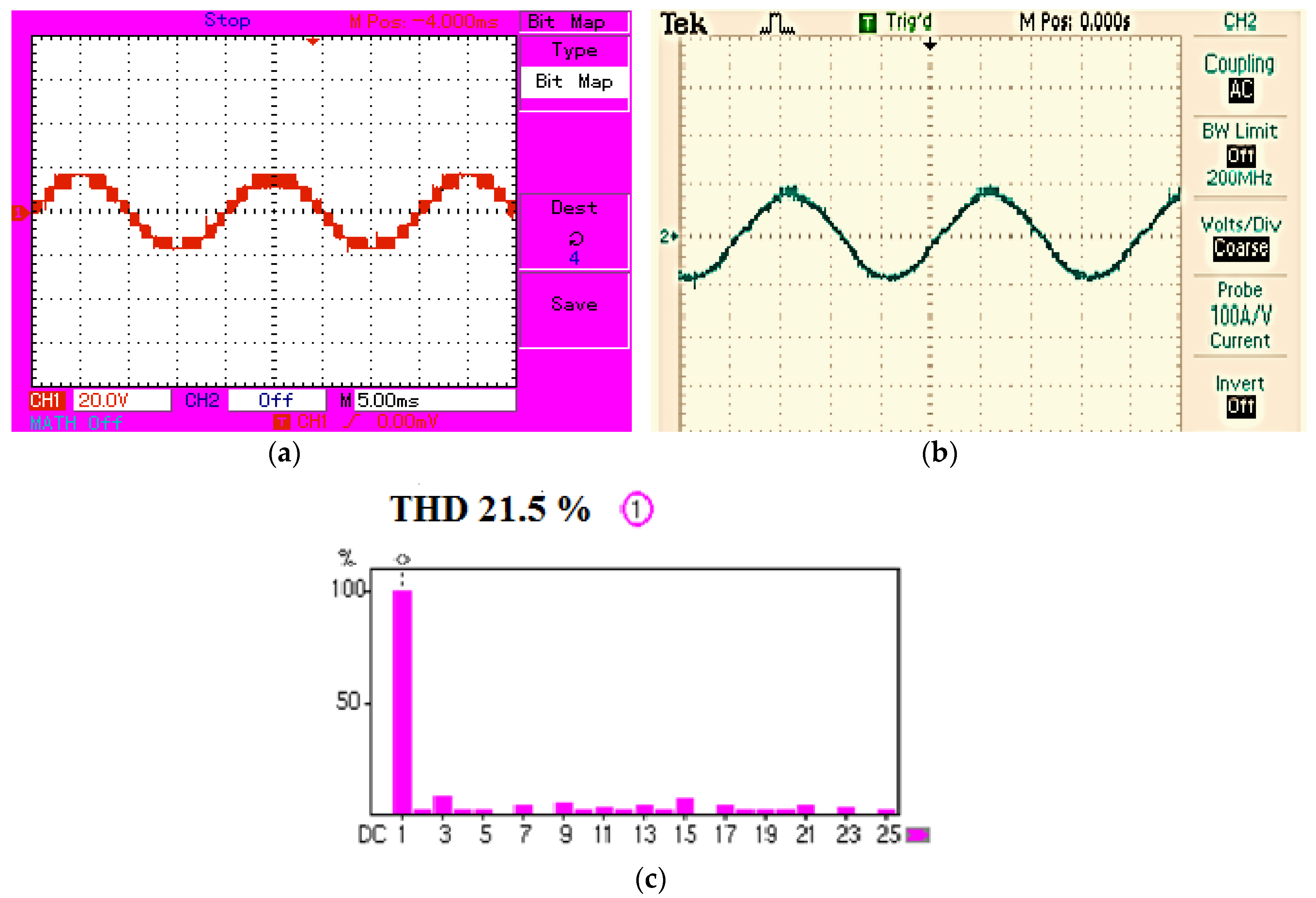
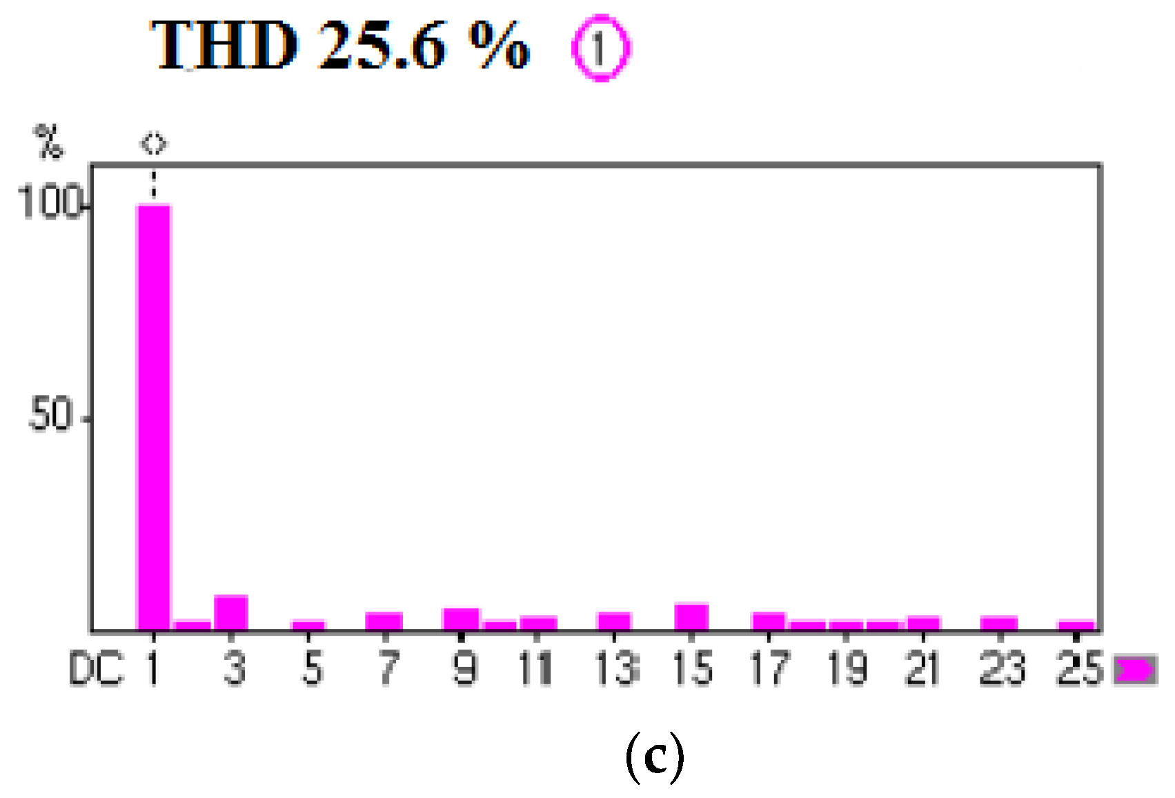
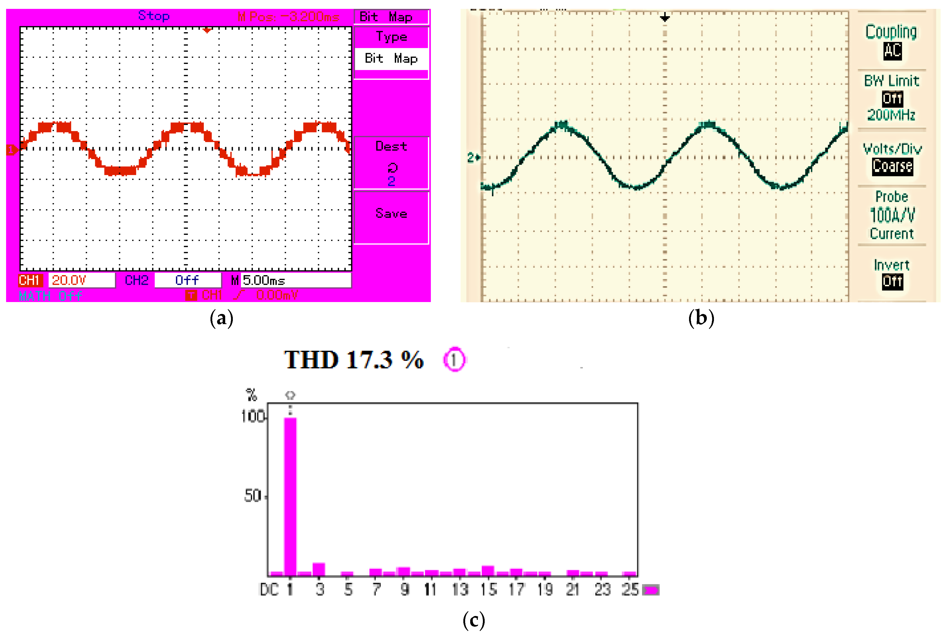
Figure 17, Figure 18, Figure 19 and Figure 20 represent the experimental output voltage, output current waveform and its corresponding voltage FFT plot for PDPWM, APODPWM, COPWM, and VFPWM strategies. All output waveforms are portrayed for ma = 0.9. From Figure 17a, Figure 18a, Figure 19a and Figure 20a, it is observed that the peak-to-peak output voltage is 36 V, which is identical to the simulation results. An amplitude of each level is 6 V. From Figure 17b, Figure 18b, Figure 19b and Figure 20b, it is evident that the experimental and simulation output currents are identical. The %THD values for different strategies are observed in Figure 17c, Figure 18c, Figure 19c and Figure 20c. The value of %THD for PD, APOD, CO, and VF PWM are 21.6%, 21.5%, 25.8%, and 17.3%, respectively. Table 2 and Figure 21a show the comparison results of the %THD output voltage with various modulation indices for different PWM strategies. Table 3 and Figure 21b show the comparison results of the VRMS output voltage with various modulation indices for different PWM strategies. Table 4 and Figure 21c show the comparison of the %DF output voltage with various modulation indices for different PWM strategies. From the results and comparison table, it is evident that the harmonic content of the output voltage is comparatively lower for the VFPWM strategy and the VRMS output voltage for the COPWM strategy is higher than the other PWM strategies. In addition, from the results, the %DF is lower in the PDPWM strategy than the other PWM strategies.
6. Conclusions
Asymmetric MLIs produce a higher output voltage level than symmetric MLIs. The selected reduced switch asymmetric MLI requires fewer components than conventional MLI topologies such as DCMLI and FCMLI. It requires only eight switches for generating the seven-level output voltage. The working principle of the selected topology and its mathematical expressions with respect to the maximum possible steps, the level of an output voltage, the magnitude value of the DC source, and the magnitude value of the maximum output voltage have been discussed. The sub-multilevel inverter of the reduced switch topology operated at a higher switching frequency whereas the H bridge operated at the fundamental switching frequency. The topology was examined with the different multi-carrier unipolar trapezoidal PWM strategies, such as PDPWM, APODPWM, COPWM, and VFPWM for generating the seven-level output voltage. By using the unipolar method, the carrier count was reduced by half compared with the conventional PWM method. The logic diagram for generating the switching pulses for the topology has been presented. The topology was examined with different modulation index values from 0.8 to 1 for checking the potential of the reduced switch topology. It was designed using Matlab/Simulink (2009b) and implemented using the SPARTAN-3 FPGA system for the laboratory-based experimental results. Various performance parameters such as %THD, VRMS, and %DF were evaluated for different strategies and compared with each other. From the results and discussion, it is evident that the VFPWM strategy produces less harmonic content than the other strategies. The COPWM strategy provides higher VRMS than the other strategies. The simulation and experimental results were found to be satisfactory.
Author Contributions
All authors contributed to the research investigation equally and presented in the current version of the full article.
Funding
There is no funding resources for the presented research work.
Conflicts of Interest
The authors declare no conflict of interest.
References
- Rodríguez, J.; Lai, J.S.; Peng, F.Z. Multilevel inverters: A survey of topologies; controls, and applications. IEEE Trans. Ind. Elecrtron. 2002, 49, 724–738. [Google Scholar]
- Malinowski, M.; Gopakumar, K.; Rodriguez, J.; Pérez, M.A. A survey on cascaded multilevel inverters. IEEE Trans. Ind. Electron. 2010, 57, 2197–2206. [Google Scholar] [CrossRef]
- Bhagwat, P.M.; Stefanovic, V.R. Generalized structure of a multilevel PWM inverter. IEEE Trans. Ind. Appl. 1983, 19, 1057–1069. [Google Scholar] [CrossRef]
- Veenstra, M.; Rufer, A. Control of a hybrid asymmetric multilevel inverter for competitive medium-voltage industrial drives. IEEE Trans. Ind. Appl. 2005, 41, 655–664. [Google Scholar] [CrossRef]
- Sanjeevikumar, P.; Michael, P. An isolated/non-isolated novel multilevel inverter configuration for a dual three-phase symmetrical/asymmetrical star-winding converter. Eng. Sci. Technol. Int. J. 2016, 19, 1763–1770. [Google Scholar]
- Prabaharan, N.; Palanisamy, K. A comprehensive review on reduced switch multilevel inverter topologies, modulation techniques and applications. Renew. Sustain. Energy Rev. 2017, 76, 1248–1282. [Google Scholar] [CrossRef]
- Rathore, A.K.; Holtz, J.; Boller, T. Generalized optimal pulse width modulation of multilevel inverters for low-switching-frequency control of medium-voltage high-power industrial AC drives. IEEE Trans. Ind. Elecrtron. 2013, 60, 4215–4224. [Google Scholar] [CrossRef]
- Prabaharan, N.; Palanisamy, K. Comparative analysis of symmetric and asymmetric reduced switch multilevel inverter topologies using unipolar pulse width modulation strategies. IET Power Electron. 2016, 9, 2808–2823. [Google Scholar] [CrossRef]
- Farakhor, A.; Ahrabi, R.R.; Ardi, H.; Ravadanegh, S.N. Symmetric and asymmetric transformer based cascaded multilevel inverter with minimum number of components. IET Power Electron. 2015, 8, 1052–1060. [Google Scholar] [CrossRef]
- Nami, A.; Zare, F.; Ghosh, A.; Blaabjerg, F. A hybrid cascade converter topology with series-connected symmetrical and asymmetrical diode-clamped H-bridge cells. IEEE Trans. Power Electron. 2011, 26, 51–65. [Google Scholar] [CrossRef] [Green Version]
- Babaei, E.; Laali, S.; Bayat, Z. A single-phase cascaded multilevel inverter based on a new basic unit with reduced number of power switches. IEEE Trans. Ind. Appl. 2014, 46, 2–4. [Google Scholar] [CrossRef]
- Behera, R.K.; Dixit, T.V.; Shyama, P.D. Analysis of experimental investigation of various carrier-based modulation schemes for three level neutral point clamped inverter fed induction motor drive. In Proceedings of the International Conference on Power Electronic, Drives and Energy Systems, New Delhi, India, 12–15 December 2006. [Google Scholar] [CrossRef]
- Dixon, J.; Pereda, J.; Castilla, C.; Bosch, S. Asymmetrical multilevel inverter for traction drives using only one dc supply. IEEE Trans. Veh. Technol. 2010, 59, 3736–3743. [Google Scholar] [CrossRef]
- Rajeevan, P.P.; Gopakumar, K. A hybrid five-level inverter with common-mode voltage elimination having single voltage source for IM drive applications. IEEE Trans. Ind. Appl. 2012, 48, 2037–2047. [Google Scholar] [CrossRef]
- Banaei, M.R.; Khounjahan, H.; Salary, E. Single-source cascaded transformers multilevel inverter with reduced number of switches. IET Power Electron. 2012, 5, 1748–1753. [Google Scholar] [CrossRef]
- Choi, J.; Kang, F. Seven-level PWM inverter employing series connected capacitors paralleled to a single dc voltage source. IEEE Trans. Ind. Electron. 2015, 62, 3448–3459. [Google Scholar]
- Zhao, J.; He, X.; Zhao, R. A novel PWM control method for hybrid-clamped multilevel inverters. IEEE Trans. Ind. Electron. 2010, 57, 2365–2373. [Google Scholar] [CrossRef]
- Wang, Z.; Cui, F.; Zhang, G.; Shi, T.; Xia, C. Novel carrier-based pwm strategy with zero-sequence voltage injected for three-level npc inverter. IEEE J. Emerg. Sel. Top. Power Electron. 2016, 4, 1442–1451. [Google Scholar] [CrossRef]
- Manoharan, M.S.; Ahmed, A.; Park, J.H. A PV power conditioning system using non regenerative single-sourced trinary asymmetric multilevel inverter with hybrid control scheme and reduced leakage current. IEEE Trans. Power Electron. 2017, 32, 7602–7614. [Google Scholar] [CrossRef]
- Wu, H.; Zhu, L.; Yang, F.; Mu, T.; Ge, H. Dual-DC-Port asymmetrical multilevel inverters with reduced conversion stages and enhanced conversion efficiency. IEEE Trans. Ind. Electron. 2017, 64, 2081–2091. [Google Scholar] [CrossRef]
- Al-Hitmi, M.; Ahmad, S.; Iqbal, A.; Sanjeevikumar, P.; Ashraf, I. Selective Harmonic Elimination in a Wide Modulation Range Using Modified Newton-Raphson and Pattern Generation Methods for a Multilevel Inverter. Energies 2018, 11, 458. [Google Scholar] [CrossRef]
- McGrath, B.P.; Holmes, D.G. Multicarrier PWM strategies for multilevel inverters. IEEE Trans. Ind. Electron. 2002, 49, 858–867. [Google Scholar] [CrossRef]
- Vargas-Merino, F.; Meco-Gutiérrez, M.J.; Heredia-Larrubia, J.R.; Ruiz-Gonzalez, A. Low switching PWM strategy using a carrier wave regulated by the slope of a trapezoidal modulator wave. IEEE Trans. Ind. Electron. 2009, 56, 2270–2274. [Google Scholar] [CrossRef]
- Sanjeevikumar, P.; Blaabjerg, F.; Wheeler, P.W.; Ojo, J.O. Three-phase multilevel inverter configuration for open-winding high power application. In Proceedings of the IEEE 6th International Symposium on Power Electronics for Distributed Generation Systems (PEDG), Aachen, Germany, 22–25 June 2015; pp. 812–815. [Google Scholar]
- Prabaharan, N.; Jerin, A.R.; Palanisamy, K. Asymmetric multilevel inverter structure with hybrid PWM strategy. Int. J. Appl. Eng. Res. 2015, 10, 2672–2676. [Google Scholar]
- Prabaharan, N.; Fathima, A.H.; Palanisamy, K. New hybrid multilevel inverter with reduced switch count using carrier based pulse width modulation technique. In Proceedings of the IEEE Conference on Energy Conversion (CENCON), Johor Bahru, Malaysia, 19–20 October 2015; pp. 176–180. [Google Scholar]
- Prabaharan, N.; Arun, V.; Palanisamy, K.; Sanjeevikumar, P. A New Pulse Width Modulation Technique with Hybrid Carrier Arrangement for Multilevel Inverter Topology. Adv. in Electron. Commun. Comput. 2018, 4, 37–44. [Google Scholar]
- Prabaharan, N.; Palanisamy, K. Analysis of Cascaded H-Bridge Multilevel Inverter Configuration with Double Level Circuit. IET Power Electron. 2017, 10, 1023–1033. [Google Scholar] [CrossRef]
- Prabaharan, N.; Arun, V.; Chinnadurai, T.; Arulkumar, K.; Jerin, A.R.; Palanisamy, K. Analysis of Symmetric Multilevel Inverter Using Unipolar Pulse Width Modulation For Photovoltaic Application. Comptes rendus de l’Acad´emie bulgare des Sciences 2018, 71, 252–260. [Google Scholar]
Figure 1.
Single phase asymmetric seven-level inverter.

Figure 2.
Carrier arrangement for the PDPWM strategy.

Figure 3.
Carrier arrangement for the APODPWM strategy.

Figure 4.
Carrier arrangement for the COPWM strategy.

Figure 5.
Carrier arrangement for the VFPWM strategy.

Figure 6.
Logic circuits for pulse width modulation (PWM) generation.

Figure 7.
Output waveform for the PDPWM strategy. (a) Voltage; (b) Current.

Figure 8.
Fast Fourier transform (FFT) plot for the output voltage of the PDPWM strategy.

Figure 9.
Output waveform for the APODPWM strategy. (a) Voltage; (b) Current.

Figure 10.
FFT plot for the output voltage of the APODPWM strategy.

Figure 11.
Output waveform for the COPWM strategy. (a) Voltage; (b) Current.

Figure 12.
FFT plot for the output voltage of the COPWM strategy.

Figure 13.
Output waveform for the VFPWM strategy. (a) Voltage; (b) Current.

Figure 14.
FFT plot for the output voltage of the VFPWM strategy.

Figure 15.
Different parameters for different modulation indices by simulation results: (a) %THD; (b) VRMS; (c) %DF; (d) %Harmonic content for different harmonic orders.
Figure 15.
Different parameters for different modulation indices by simulation results: (a) %THD; (b) VRMS; (c) %DF; (d) %Harmonic content for different harmonic orders.

Figure 16.
Laboratory-based experimental setup for asymmetric reduced switch multilevel inverter.

Figure 17.
Experimental output waveform for the PDPWM strategy. (a) Voltage; (b) Current; (c) FFT plot for the output voltage.
Figure 17.
Experimental output waveform for the PDPWM strategy. (a) Voltage; (b) Current; (c) FFT plot for the output voltage.


Figure 18.
Experimental output waveform for the APODPWM strategy. (a) Voltage; (b) Current; (c) FFT plot for the output voltage.
Figure 18.
Experimental output waveform for the APODPWM strategy. (a) Voltage; (b) Current; (c) FFT plot for the output voltage.

Figure 19.
Experimental output waveform for the COPWM strategy. (a) Voltage; (b) Current; (c) FFT plot for the output voltage.
Figure 19.
Experimental output waveform for the COPWM strategy. (a) Voltage; (b) Current; (c) FFT plot for the output voltage.


Figure 20.
Experimental output waveform for the VFPWM strategy. (a) Voltage; (b) Current; (c) FFT plot for the output voltage.
Figure 20.
Experimental output waveform for the VFPWM strategy. (a) Voltage; (b) Current; (c) FFT plot for the output voltage.

Figure 21.
Different parameters for different modulation indices using experimental results: (a) %THD; (b) VRMS; (c) %DF.
Figure 21.
Different parameters for different modulation indices using experimental results: (a) %THD; (b) VRMS; (c) %DF.


Table 1.
Switching states for reduced switch multilevel inverter (MLI).
| S1 | S2 | S3 | S4 | A1 | A2 | B1 | B2 | Output Level (Vout) |
|---|---|---|---|---|---|---|---|---|
| 1 | 0 | 0 | 1 | 1 | 1 | 0 | 0 | +3 Vdc |
| 1 | 0 | 1 | 0 | 1 | 1 | 0 | 0 | +2 Vdc |
| 0 | 1 | 0 | 1 | 1 | 1 | 0 | 0 | +1 Vdc |
| 0 | 1 | 1 | 0 | 1 | 1 | 0 | 0 | 0 |
| 0 | 1 | 0 | 1 | 0 | 0 | 1 | 1 | −1 Vdc |
| 1 | 0 | 1 | 0 | 0 | 0 | 1 | 1 | −2 Vdc |
| 1 | 0 | 0 | 1 | 0 | 0 | 1 | 1 | −3 Vdc |
Table 2.
%THD for different modulation indices.
| Simulation Results | Experimental Results | |||||||
|---|---|---|---|---|---|---|---|---|
| ma | PD | APOD | CO | VF | PD | APOD | CO | VF |
| 1 | 15.33 | 15.78 | 21.11 | 14.51 | 16.5 | 16.8 | 21.7 | 14.8 |
| 0.95 | 19.13 | 19.09 | 23.56 | 17.96 | 20.0 | 19.4 | 23.8 | 18.2 |
| 0.9 | 21.51 | 21.03 | 25.63 | 20.06 | 21.6 | 21.5 | 25.8 | 21.2 |
| 0.85 | 23.53 | 23.44 | 28.33 | 23.18 | 23.8 | 24 | 28.7 | 23.8 |
| 0.8 | 24.70 | 24.84 | 30.46 | 25.26 | 24.9 | 25.1 | 31 | 25.6 |
Table 3.
VRMS for different modulation indices.
| Simulation Results | Experimental Results | |||||||
|---|---|---|---|---|---|---|---|---|
| ma | PD | APOD | CO | VF | PD | APOD | CO | VF |
| 1 | 12.734 | 12.8 | 13.54 | 13.36 | 13.1 | 13.0 | 13.7 | 13.5 |
| 0.95 | 12.72 | 12.72 | 13.03 | 12.75 | 12.9 | 12.8 | 13.2 | 12.8 |
| 0.9 | 12.03 | 12.06 | 12.54 | 12.13 | 12.1 | 12.3 | 12.9 | 12.4 |
| 0.85 | 11.37 | 11.36 | 11.88 | 11.42 | 11.7 | 11.6 | 12.0 | 11.8 |
| 0.8 | 10.72 | 10.69 | 11.32 | 10.71 | 10.9 | 10.8 | 11.5 | 10.9 |
Table 4.
%Distortion factor for different modulation indices.
| Simulation Results | Experimental Results | |||||||
|---|---|---|---|---|---|---|---|---|
| ma | PD | APOD | CO | VF | PD | APOD | CO | VF |
| 1 | 0.1798209 | 0.1747 | 0.3098 | 0.2333 | 0.181 | 0.183 | 0.291 | 0.272 |
| 0.95 | 0.1719129 | 0.1714 | 0.3401 | 0.2119 | 0.180 | 0.181 | 0.311 | 0.217 |
| 0.9 | 0.1564152 | 0.1716 | 0.4262 | 0.2092 | 0.160 | 0.178 | 0.399 | 0.210 |
| 0.85 | 0.1612577 | 0.1698 | 0.5707 | 0.1892 | 0.165 | 0.171 | 0.491 | 0.191 |
| 0.8 | 0.1783759 | 0.1681 | 0.7031 | 0.1539 | 0.181 | 0.170 | 0.575 | 0.165 |
© 2018 by the authors. Licensee MDPI, Basel, Switzerland. This article is an open access article distributed under the terms and conditions of the Creative Commons Attribution (CC BY) license (http://creativecommons.org/licenses/by/4.0/).
Share and Cite
MDPI and ACS Style
Prabaharan, N.; Arun, V.; Sanjeevikumar, P.; Mihet-Popa, L.; Blaabjerg, F. Reconfiguration of a Multilevel Inverter with Trapezoidal Pulse Width Modulation. Energies 2018, 11, 2148. https://doi.org/10.3390/en11082148
AMA Style
Prabaharan N, Arun V, Sanjeevikumar P, Mihet-Popa L, Blaabjerg F. Reconfiguration of a Multilevel Inverter with Trapezoidal Pulse Width Modulation. Energies. 2018; 11(8):2148. https://doi.org/10.3390/en11082148
Chicago/Turabian StylePrabaharan, Nataraj, V. Arun, Padmanaban Sanjeevikumar, Lucian Mihet-Popa, and Frede Blaabjerg. 2018. "Reconfiguration of a Multilevel Inverter with Trapezoidal Pulse Width Modulation" Energies 11, no. 8: 2148. https://doi.org/10.3390/en11082148
Note that from the first issue of 2016, this journal uses article numbers instead of page numbers. See further details here.