Compact Rectifier Circuit Design for Harvesting GSM/900 Ambient Energy
by
 , , and
Surajo Muhammad
1 ,
,
Jun Jiat Tiang
1, 
Sew Kin Wong
1,
Amjad Iqbal
1,*,
Mohammad Alibakhshikenari
2,* and
and
Ernesto Limiti
2
1
Centre For Wireless Technology (CWT), Faculty of Engineering, Multimedia University, Cyberjaya 63100, Malaysia
2
Electronic Engineering Department, University of Rome “Tor Vergata”, Via del Politecnico 1, 00133 Rome, Italy
*
Authors to whom correspondence should be addressed.
Electronics 2020, 9(10), 1614; https://doi.org/10.3390/electronics9101614
Submission received: 6 September 2020
/
Revised: 29 September 2020
/
Accepted: 29 September 2020
/
Published: 1 October 2020
(This article belongs to the Special Issue Recent Advances in Antenna Design for 5G Heterogeneous Networks)
Abstract
:In this paper, a compact rectifier, capable of harvesting ambient radio frequency (RF) power is proposed. The total size of the rectifier is 45.4 mm × 7.8 mm × 1.6 mm, designed on FR-4 substrate using a single-stage voltage multiplier at 900 MHz. GSM/900 is among the favorable RF Energy Harvesting (RFEH) energy sources that span over a wide range with minimal path loss and high input power. The proposed RFEH rectifier achieves measured and simulated RF-to-dc (RF to direct current) power conversion efficiency (PCE) of 43.6% and 44.3% for 0 dBm input power, respectively. Additionally, the rectifier attained 3.1 V DC output voltage across 2 k load terminal for 14 dBm and is capable of sensing low input power at −20 dBm. The work presents a compact rectifier to harvest RF energy at 900 MHz, making it a good candidate for low powered wireless communication systems as compares to the other state of the art rectifier.
1. Introduction
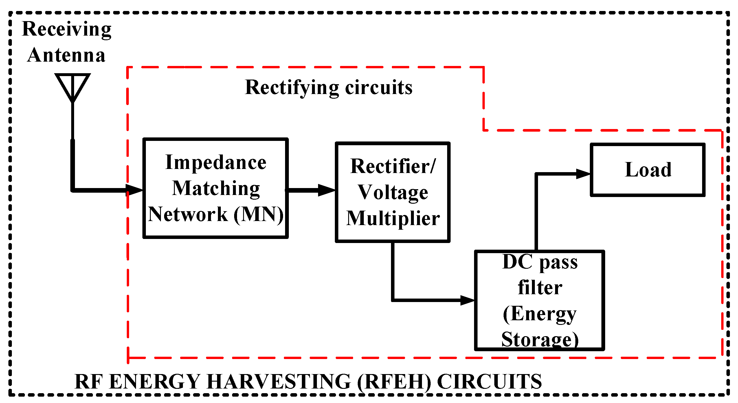
The ubiquitous nature of wireless communication technology has over the years attract and gained much attention and contribution from researchers globally [1,2]. Additionally, GSM900/1800, 3G, 4G, Wi-Fi, and the evolving auspicious 5G are among a few dominant wireless technology generation operating daily to cater for human needs and demand [3,4]. Recent development in wireless communication technology gave birth to new and evolving technological innovations. The increasing demand of such invention led to one or more application driver in the areas of IoT, industrial IoT, autonomous driving, smart farming, smart cities, and many more [5,6]. Uninterrupted power supply over remote places limits the potential of wire-based ultra-low powered IoT devices and sensor nodes. which directly restricts their capabilities for security surveillances, smart farming, and other related applications besides a copper loss [5,6,7]. One of the main challenges with the evolving ultra-low powered IoT devices is energy storage limitation. These, in turn, increase the need for RFEH systems. To over come the major challenges with traditional battery-based systems to charge/maintain/replace a battery. RFEH is believed to be a promising technology through direct power or battery recharging from abundant electromagnetic (EM) energy radiating in the environment. The technology can be deployed in low-powered devices for security surveillance, smart farming and many more [5,6,7,8]. Initially, the concept of energy harvesting started to evolve in the 1990s along with Tesla finding’s on electrical energy conversion from an EM wave [5]. RF power system typically comprises an antenna, IMN, a rectifying diode, a storage element (DC pass filter), and a terminal load. A combination of five circuit elements gives rise to rectenna. A rectenna without the antenna component is categorized as a rectifying circuits. Figure 1 provides a block diagram containing the key components of rectenna. The matching network (MN) and the rectifier circuit play an important role in the RFEH system. MN is aim at ensuring optimum energy transfer between the receiving antenna and the load, and the latter transform the scavenged RF EM signals into a usable DC output voltage. RFEH module can be deployed in a sensitive and critical environment such as autonomous driving, security surveillance, and healthcare systems, for their capability to operate under both environmental and nonenvironmental condition unlike the other forms of energy harvesting system [5]. The operation of rectifying circuit and RFEH system are generally assessed through (PCE). Several RFEH circuits design have been studied and proposed to achieve significant PCE through the use of wide-band, multi-band, dual and single band rectifiers. Among the designs, single-band rectenna used to be more efficient as compared to their wide or broad band counter parts [5,8]. The broadband rectifiers are generally associated with much more circuits complexity, which reduces the overall circuit performance because of parasitics capacitance at the junction of the diode and other lumped elements [8,9]. The authors of [10,11] designed a rectenna with maximum PCE at 37.8% and 28% using −1.5 dBm and −15 dBm input power. To recycle ambient RF signal, a rectenna with 20% efficiency is described in [12] using 62 W/cm (13.27 dBm) input power with a total geometry of 342.55 cm. Several research projects have been developed to accomplish efficient rectenna at relatively low input power [13,14]. An RF rectifier is proposed in [15], the design can achieve up to 33% efficiency at −10 dBm input power at the cost of complex circuit with large electrical length. A maximum PCE of 47.8% and 38% is highlighted in [16,17], using an input power between (5–14 dBm), respectively. The authors of [13] also worked on rectifier circuit and realized 50% maximum PCE using 21 dBm solar panel. A rectenna that achieved up to 24% PCE is proposed in [14], using −20 dBm input power with help of an antenna array and rectifier with a total geometry of 32.4 cm.
Many foregoing types of research in the RFEH system focused on a much higher frequency between GSM/1800 to WLAN/5200 to achieve compactness. The operational frequency contributed significantly to achieving a compact RFEH circuit [7,8,9,10,11,12,13,14,15,16,17,18]. The RF spectral survey from the open literature and the one carried out in this work, using (Aim TTi PSA6005 6 GHz RF spectrum analyzer), come out with a notable result surrounding the lower GSM/900 band towards generating higher available ambient RF power [14,15]. This paper, proposed a compact cm rectifier at 900 MHz using simple L-section MN. Conversely, the designed is a good candidate for harvesting RF energy in ambient environment with capability of sensing RF input power below −20 dBm integrable with low powered IoT devices. In the remaining sections of this work, Section 2 presents a rectifier circuit design and analysis, Section 3 highlights the result of a finding of the proposed rectifier and Section 4 provides the concluding remarks. The following outlines the main contribution of this work:
- To the best of our knowledge, this is the compact RFEH rectifier as compares to state of the art rectifiers at 900 MHz.
- This research targets an energy harvesting rectifier that works over GSM/900 to cover long and remote places suitable for low powered IoT devices and sensor nodes.
- The proposed design can receive an RF input signal at less than −20 dBm and also provides detailed circuit and performance analysis.
2. Rectifier Circuit Design and Analysis
The voltage appears at the end of an RFEH antenna is considerably of small quantity and as well analogous to sinusoidal signal.A conditioning circuit across the load terminal is an important figure to improve the output DC signals of the RFEH module. Diode(s), MN, and load terminal are primary components to the rectifying circuits. The diode(s) is playing a vital role in converting the accessible ambient RF power into a usable DC supply. The MN minimizes the reflection losses for RF input power received by the antenna. The low powered RFEH MN need to be simple in design with minimum losses.
2.1. Transmission Line and Input Impedance Matching Network
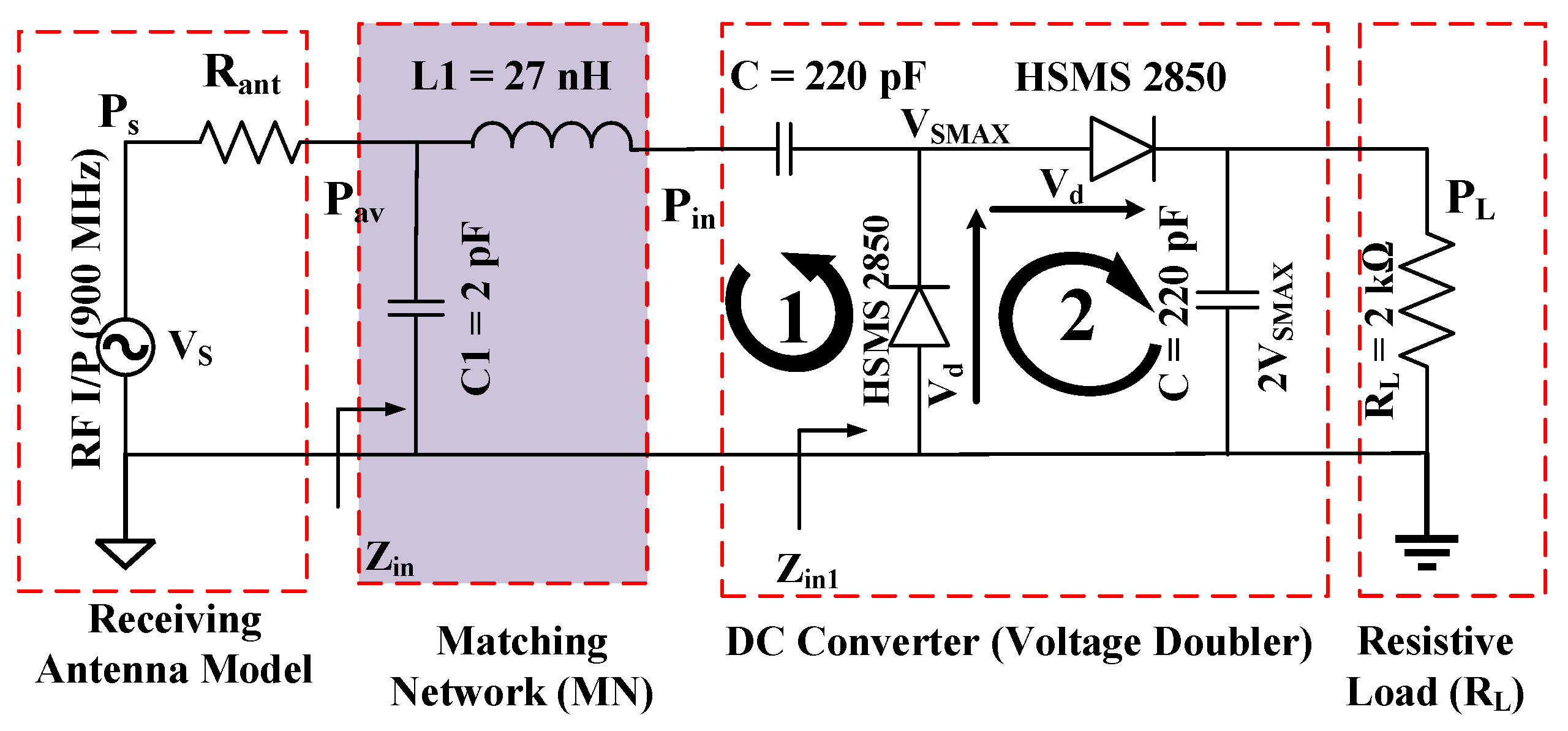
A 50 microstrip transmission line width and length to match the antenna with MN and voltage multiplier was first to design using FR-4 substrate ( = 5.4, h = 1.6 mm, and tan = 0.02). The substrate is chosen for its low cost, light weight, and ease of fabrication [7]. ADS LineCal operator is applied to compute and optimized the proposed width and length of the line at 2.7 mm and 30 mm, respectively. MN is significant part of the rectifier circuits. The design process of MN is a challenging task because the rectifier input impedance () is controlled by: operating frequency (), input power (), diode inconstant internal resistance () and terminal load () [19].
Figure 2 shows L-section MN to match the impedances between the source and the load. The proposed model reduces circuit complexity using two simple inductive () and capacitive () reactive elements. The inductor () plays a vital role towards enhancing the input signal getting into the rectifier and the capacitor () enhances the rectifier matching [19]. The MN parameters can be computed by negating source and load imaginary part and equating their real part at the design frequency as illustrated in Equations (1)–(5). The equivalent power source from the antenna () is analogous to the antenna available power () passing through the transmission line and the MN. Other related reference power notation in the circuit model includes rectifier input power () and the output power consumed by the load terminal ().
Equating the real part of the antenna with the rectifier input impedance we get:
where = rectifier input impedance, = source impedance, and the quality factor Q is given by:
To determine the reactance parameters, the quality factor Q can be express as the ratio of imaginary (reactive) part of the impedance to the respective real (resistive) components as:
where = reactive components of the load impedance operating at frequency , using Equation (3) the inductance of the network is given as:
L-section capacitance can be computed by setting the imaginary part of Equation (3) to zero as:
A two-element MN ( and ) is designed at 900 MHz using a 50 transmission line as (), terminated with a 2 k load. The numerical values of and were computed at 55 nH and 0.5 pF, respectively. The parameters were transfer into ADS simulation software using ideal component palette. Because of the effects of the transmission line in the circuits, the lumped elements need to be tune and optimize. () and () were compensated with −10 nH and +0.5 pF, and the rectifier is matched at 45 nH and 1 pF, respectively. The circuit is further tuned by replacing the ideal elements with equivalent surface mount device (SMD) in the ADS library at 27 nH and 2 pF.
2.2. Rectifier Design
Rectifying circuits are of different configuration layout. The circuits can be achieved as a single series or shunt rectifier diode, voltage doubler rectifiers, up to the level of multistage and cascaded rectifiers. The authors of [9] highlights an extensive study on various types of rectifier circuits topology. Rectifier selection to operate at high frequency need to have: reliable power response, and the ability to manage power with minimal dissipation [7] for efficient and effective power harvesting. A single-stage voltage multiplier configuration is a suitable candidate to be deployed in RFEH circuits as compared to a single series/shunt half-wave configurations. An RF rectifier circuit with a single-stage voltage multiplier is more efficient with higher output power compares with single series/shunt half-wave rectifiers. Single-stage voltage multiplier rectifiers also offer fewer losses in contrast to multistage rectifiers for a low-powered RF harvester [9]. The proposed rectifier is built based on a voltage multiplier topology with a pair of HSMS-2850 diode (SOT-323 layout), as shown in Figure 2. The diode is a suitable candidate for low power RF application with a small junction capacitance of 0.18 pF and a minimum detectable voltage of 150 mV at 0.1 mA [5]. The rectifier junction capacitance (C) is controlled by the operating frequency and voltage as express in Equation (6).
where C is the capacitance of the capacitor with current I passing through junction diode at the rate of non linear voltage “V”.
The antenna then receives and transmits the reactive power into the rectifier as express by the equivalent wave Equation (7) [9]. During the negative half-wave AC circle diode , become forward bias and charges (C) in label (1) to (). At the positive half-wave AC cycle, diode is reverse bias blocking the voltage in label (1) from discharging, and diode in label (2) change into forward bias. The reserve () in label (1) and diode synchronously sum up the output voltage to () onto the capacitor (C) in label (2), which discharges through the load terminal () as describe in Equations (8) and (9).
where is the amplitude of the RF input signal received at the output of the MN operating at frequency [20].
where is the forward bias voltage of the rectifying diode, and
3. Results and Discussion
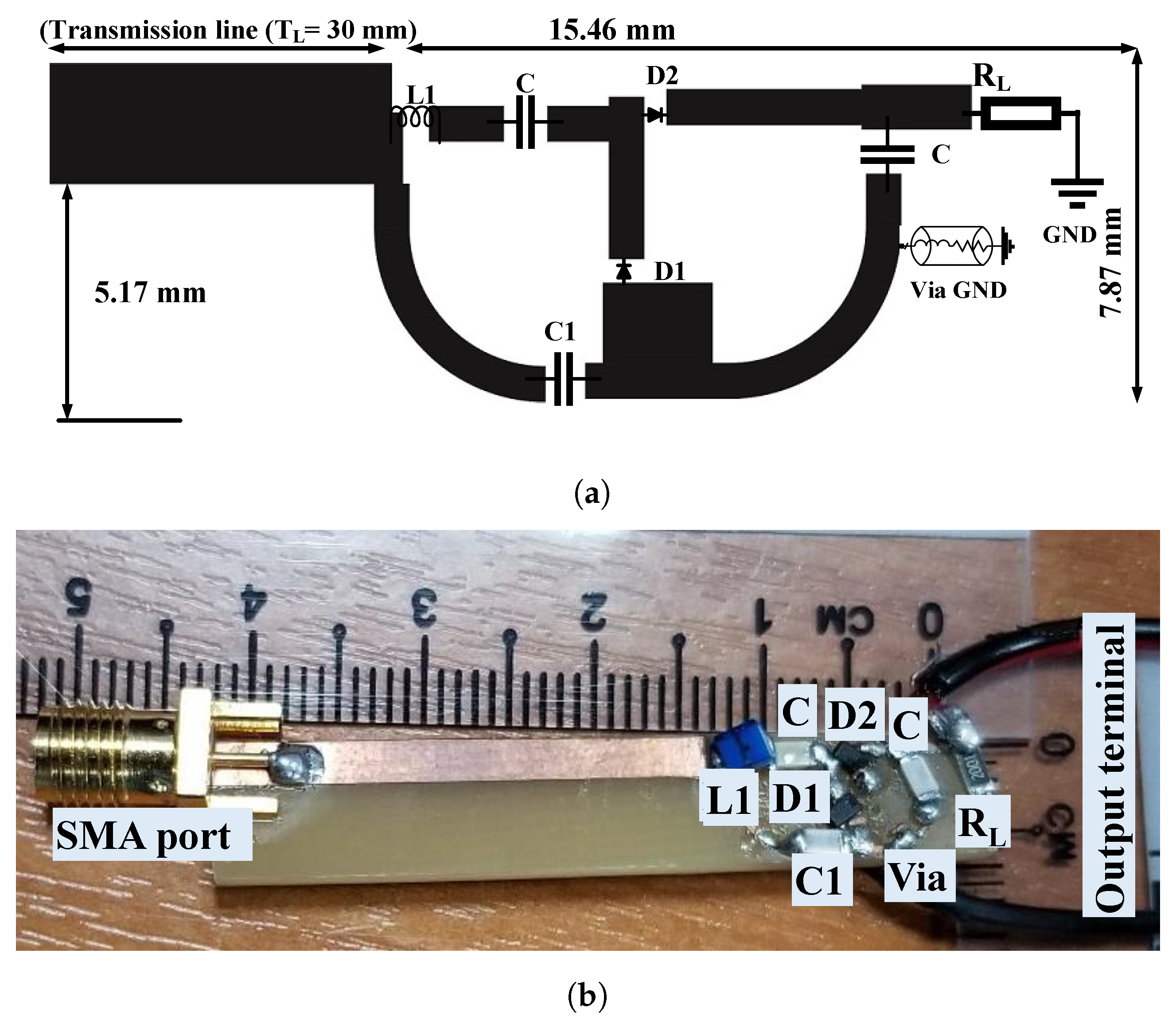
The propose rectifier is fabricated on a low-cost commercial FR-4 board with a total dimension 45.4 mm × 7.8 mm × 1.6 mm connected via 50 SMA probe. A pair of small crocodile clip is used to connect the rectifier across the load terminal to measure the output parameters as seen in Figure 3b. Figure 3a also provides layout model of the rectifier prototype.
Equation (10) provides a wheeler’s transmission line width equation that portrays the effects of (W) on the rectifier matching [21]. Decreasing (W) below the designed value causes a direct rectifier mismatch at the proposed frequency. Increasing (W) above the designed value shifted the rectifier operating frequency by 20 MHz in addition to impedance mismatch. The transmission line length is computed through a guided wave at = 42.5 mm and is optimized at 30 mm.
where is the characteristic impedance of the line, W = width of transmission line, h = height of the substrate, and gives the effective dielectric constant of the substrate.
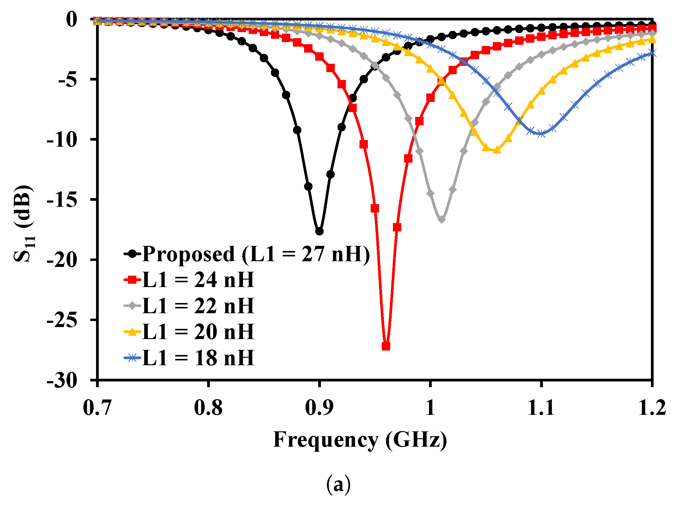
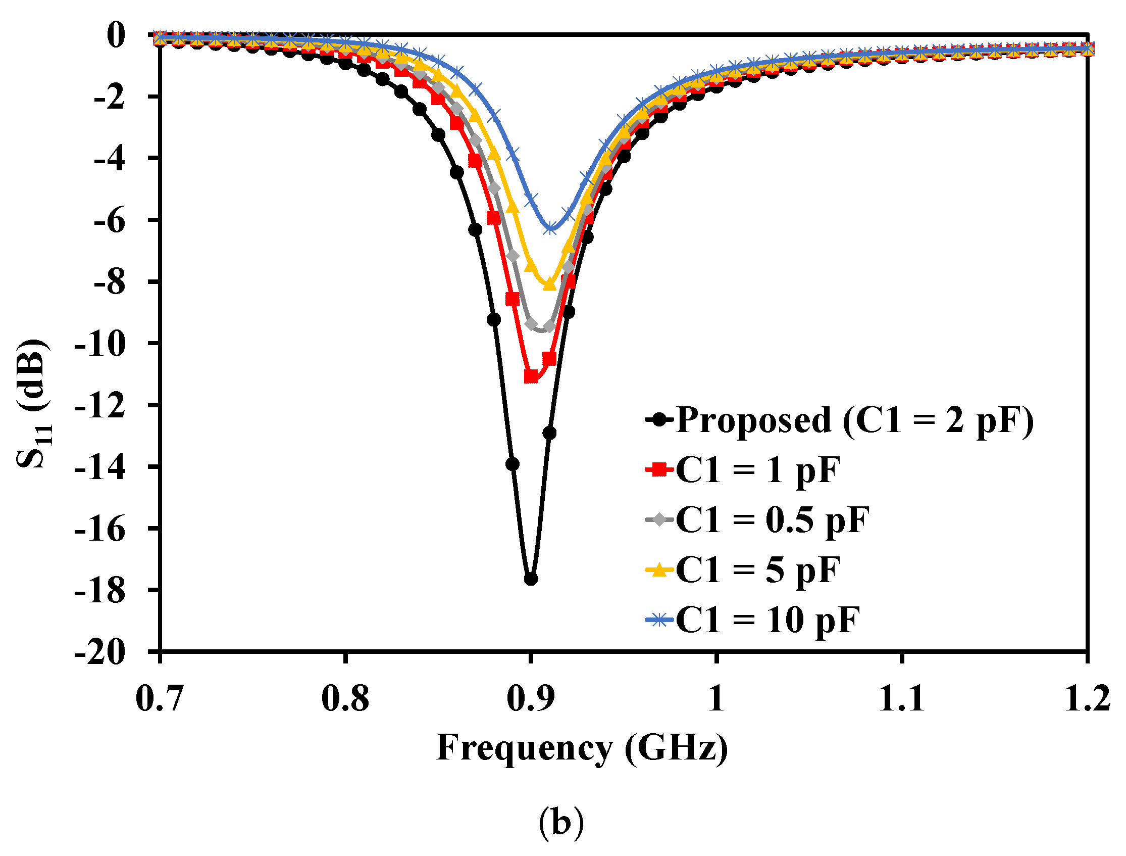
To evaluate the rectifier performance at the design frequency, L-section MN undergo a parametric study. Figure 4a depicts the simulated reflection coefficient versus frequency at different values of the inductor (). The design frequency shifted to about 1.1 GHz for an inductance value from 27 nH to 18 nH. Following the inductive reactance properties, frequency increases the current flowing through the inductor, which lowers the inductance value in the circuits [3,4,5,13]. Figure 4b also shows the effect of capacitance () in the MN, varying the capacitance from 2 pF to 10 pF deteriorates the rectifier matching. Hence, lowering or increasing the capacitance value leads to rectifier mismatched which can render the rectifying circuit inefficient [9,20].
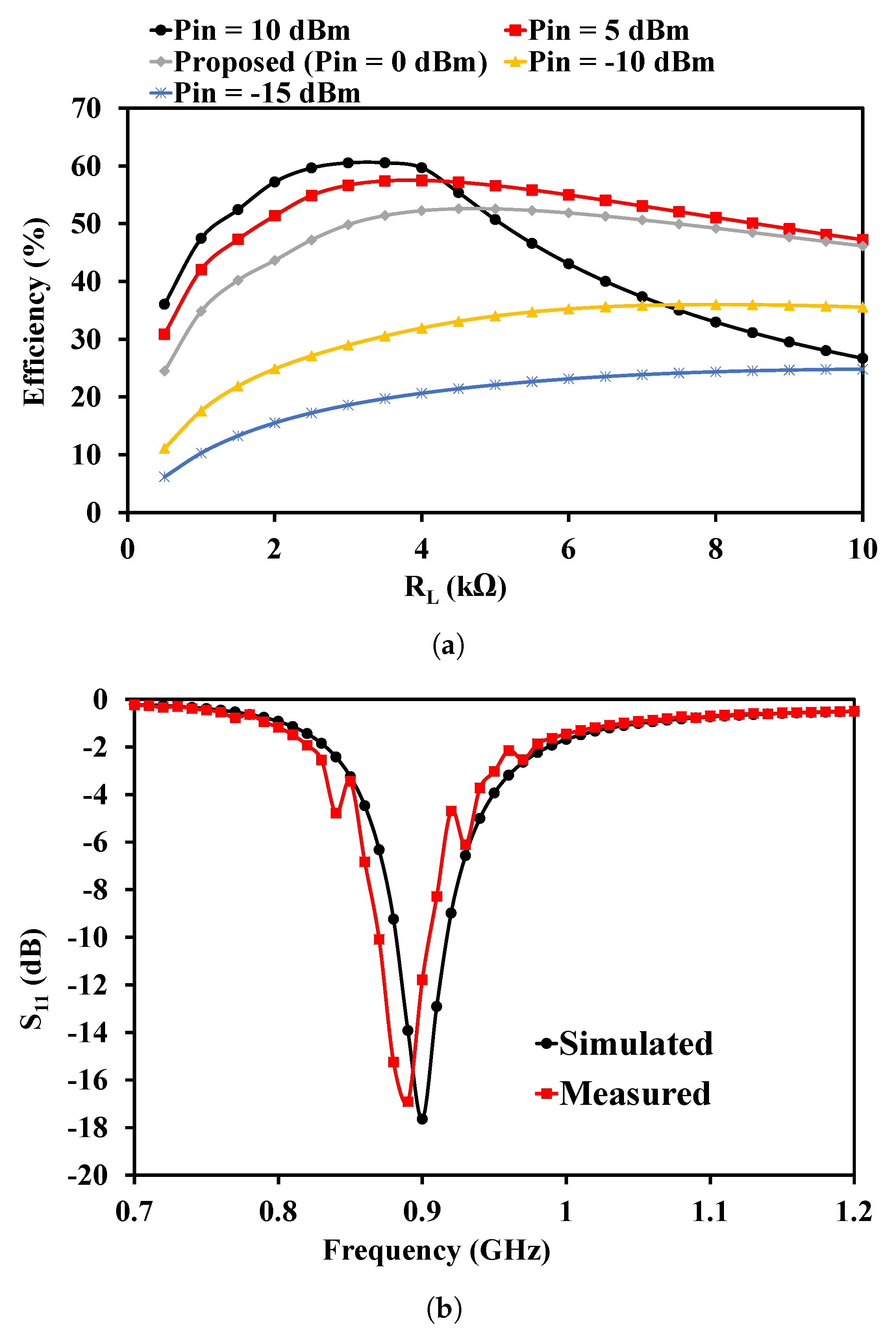
To analyze the PCE of the proposed rectifier, Figure 5a presents the result of the load terminal () sweep at various input power levels (from −15 dBm to 10 dBm in step of 5 dBm). The result shows that the efficiency increases with an increase of input power across the load which agreed well with Equation (7) [5,6,7,8,9,10,11,12,13,14,15,16,17,18,19,20,21,22]. The rectifier achieves a maximum PCE along the 2–4 k load terminal in both cases. The design shows a low PCE for −15 dBm with an efficiency greater than 20% for a load above 2.5 k. A 60% high efficiency is also observed around the 2–4 k load for +10 dBm input power.
Figure 5b presents the simulated and measured reflection coefficient () of the proposed rectifier at 900 MHz. The design achieved a simulated and measured −10 dB bandwidth of 45 MHz (880–925 MHz) and 46 MHz (870–916 MHz) respectively. A vector network analyzer (E5062A) from Agilent Technologies is used to measure the () of the rectifier for −20 dBm input power level.
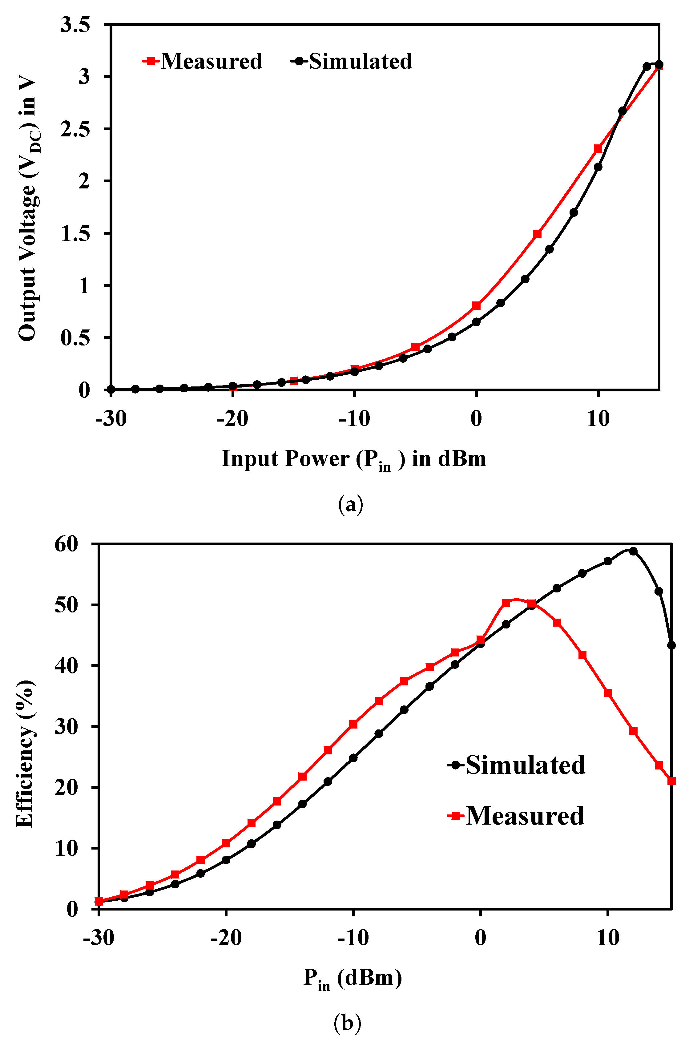
Equation (12) provides a relation that describes the rectifier ability in converting the received RF signal in to a usable output DC signal known as (PCE) in terms of output and input power. To determine the simulated output DC voltage and efficiency over a range of frequency, input power and a terminal load. A large signal s-parameter (LSSP) and harmonic balance (HB) simulation modules’s that coexist in ADS is deployed into the design owing to the non-linear characteristics of the rectifying diode [5,6,7,8,9,10,11]. A 12 GHz APSIN12G signal generator sweep from −30 dBm to 10 dBm input power is used to measure the rectifier output DC voltage across the 2 k load terminal. The measured result is in good agreement with simulation, as depicted in Figure 6a. The rectifier can receive an RF input signal at −30 dBm with the capability of harvesting 3.1 V for both simulated and measured results at 14 dBm and 16 dBm, respectively. Equation (11) provides the rectifier output DC voltage from Equation (9) [9,23].
where is the power conversion efficiency, is DC output power across the load and gives the output DC voltage.
Figure 6b presents the simulated and measured PCE across the 2 k load terminal, and the rectifier achieves a PCE of 44.3% and 43.6% for 0 dBm input power, respectively. The rectifier experiences a drop in measured efficiency because of nonlinear characteristics of the diode as reported in the datasheet, in connection with other losses from the circuit board (Such as SMA connector probe, interconnecting transmission lines, soldering, and chip-component tolerant losses) [3].
Table 1 provides a comparison table of the proposed design with other related works in the literature. The authors of [10,11] presents an energy harvester with about times larger in electrical length than the proposed design. The authors of [13] did not record the amount of input power at which the rectifier achieves its maximum PCE, but uses a solar antenna [24] with 21 dBm capacity and a much larger rectifier. The authors of [14] also comes out with a harvesting circuit without describing the MN used besides rectifier large electrical length. A much lower PCE at high input power is reported in [16,17]. The proposed design in the open literature target high-frequency band rectifier starting from GSM/1800—WLAN/5200 which contributes to achieving rectifier compactness. The proposed design in this work offers a compact size rectifier capable of harvesting RF signal over a long-range cover by GSM/900.
4. Conclusions
This paper, proposes the design and construction of a compact rectifier at a 900 MHz GSM band, using HSMS-2850 Schottky diode. A transmission line and an L-section impedance matching network are designed from the closed-form equations, to match the input impedance of the rectifier with 50 . The circuit undergoes parametric tuning from an ideal to model component to achieve better performance and minimizes the effects of the transmission line in the network. The fabricated prototype can receive an ambient RF signal below −20 dBm and achieved 50.2% and 49.1% maximum PCE for both simulated and measured results at 14 dBm and 2 dBm, respectively. Similarly, the circuit reaches an output DC voltage of 3.1 V for simulated and measured results at 14 dBm and 16 dBm, respectively using a 2 k load terminal. The proposed rectifier occupies a total of 351 mm (0.31 × 0.05) on the PCB circuit board, offering efficiency and compactness improvement as compares to other recent designs making it suitable for various compact energy harvesting applications.
Author Contributions
Conceptualization, S.M.; methodology, S.M. and M.A.; software, S.M.; validation, S.M., A.I., M.A. and E.L.; formal analysis, S.M.; investigation, S.M.; resources, J.J.T. and S.K.W.; data curation, S.M.; writing—original draft preparation, S.M.; writing—review and editing, S.M. and A.I.; visualization, S.M., M.A. and E.L.; supervision, J.J.T. and S.K.W.; project administration, J.J.T. and S.K.W.; funding acquisition, J.J.T. and S.K.W. All authors have read and agreed to the published version of the manuscript.
Funding
This work was supported by TM R&D Malaysia under project number MMUE/190001.
Conflicts of Interest
The authors declare no conflict of interest.
References
- Chen, Y.S.; You, J.W. A scalable and multidirectional rectenna system for RF energy harvesting. IEEE Trans. Compon. Packag. Manuf. Technol. 2018, 8, 2060–2072. [Google Scholar] [CrossRef]
- Pardue, C.A.; Bellaredj, M.L.F.; Davis, A.K.; Swaminathan, M.; Kohl, P.; Fujii, T.; Nakazawa, S. Design and characterization of inductors for self-powered IoT edge devices. IEEE Trans. Compon. Packag. Manuf. Technol. 2018, 8, 1263–1271. [Google Scholar] [CrossRef]
- Mansour, M.M.; Kanaya, H. Compact and broadband RF rectifier with 1.5 octave bandwidth based on a simple pair of L-Section matching network. IEEE Microw. Wirel. Compon. Lett. 2018, 28, 335–337. [Google Scholar] [CrossRef]
- Pardue, C.A.; Bellaredj, M.L.F.; Torun, H.M.; Swaminathan, M.; Kohl, P.; Davis, A.K. RF Wireless Power Transfer Using Integrated Inductor. IEEE Trans. Compon. Packag. Manuf. Technol. 2018, 9, 913–920. [Google Scholar] [CrossRef]
- Awais, Q.; Jin, Y.; Chattha, H.T.; Jamil, M.; Qiang, H.; Khawaja, B.A. A compact rectenna system with high conversion efficiency for wireless energy harvesting. IEEE Access 2018, 6, 35857–35866. [Google Scholar] [CrossRef]
- Wong, S.W.; Sun, G.H.; Zhu, L.; Chen, Z.N.; Chu, Q.X. Integration of Wireless Coil and Bluetooth Antenna for High Charging and Radiation Efficiencies. IEEE Trans. Compon. Packag. Manuf. Technol. 2018, 8, 1292–1299. [Google Scholar] [CrossRef]
- Mansour, M.M.; Kanaya, H. Novel L-Slot Matching Circuit Integrated with Circularly Polarized Rectenna for Wireless Energy Harvesting. Electronics 2019, 8, 651. [Google Scholar] [CrossRef] [Green Version]
- Liu, J.; Zhang, X.Y. Compact triple-band rectifier for ambient RF energy harvesting application. IEEE Access 2018, 6, 19018–19024. [Google Scholar] [CrossRef]
- Song, C.; Huang, Y.; Carter, P.; Zhou, J.; Yuan, S.; Xu, Q.; Kod, M. A novel six-band dual CP rectenna using improved impedance matching technique for ambient RF energy harvesting. IEEE Trans. Antennas Propag. 2016, 64, 3160–3171. [Google Scholar] [CrossRef] [Green Version]
- Huang, F.J.; Yo, T.C.; Lee, C.M.; Luo, C.H. Design of circular polarization antenna with harmonic suppression for rectenna application. IEEE Antennas Wirel. Propag. Lett. 2012, 11, 592–595. [Google Scholar] [CrossRef]
- Palazzi, V.; Kalialakis, C.; Alimenti, F.; Mezzanotte, P.; Roselli, L.; Collado, A.; Georgiadis, A. Design of a ultra-compact low-power rectenna in paper substrate for energy harvesting in the Wi-Fi band. In Proceedings of the 2016 IEEE Wireless Power Transfer Conference (WPTC), Aveiro, Portugal, 5–6 May 2016; pp. 1–4. [Google Scholar]
- Falkenstein, E.; Roberg, M.; Popovic, Z. Low-power wireless power delivery. IEEE Trans. Microw. Theory Tech. 2012, 60, 2277–2286. [Google Scholar] [CrossRef]
- Niotaki, K.; Georgiadis, A.; Collado, A.; Vardakas, J.S. Dual-band resistance compression networks for improved rectifier performance. IEEE Trans. Microw. Theory Tech. 2014, 62, 3512–3521. [Google Scholar] [CrossRef] [Green Version]
- Adam, I.; Yasin, M.N.M.; Rahim, H.A.; Soh, P.J.; Abdulmalek, M.F. A compact dual-band rectenna for ambient RF energy harvesting. Microw. Opt. Technol. Lett. 2018, 60, 2740–2748. [Google Scholar] [CrossRef]
- Masotti, D.; Costanzo, A.; Francia, P.; Filippi, M.; Romani, A. A load-modulated rectifier for RF micropower harvesting with start-up strategies. IEEE Trans. Microw. Theory Tech. 2014, 62, 994–1004. [Google Scholar] [CrossRef]
- Lu, J.J.; Yang, X.X.; Mei, H.; Tan, C. A four-band rectifier with adaptive power for electromagnetic energy harvesting. IEEE Microw. Wirel. Compon. Lett. 2016, 26, 819–821. [Google Scholar] [CrossRef]
- Hsu, C.Y.; Lin, S.C.; Tsai, Z.M. Quadband rectifier using resonant matching networks for enhanced harvesting capability. IEEE Microw. Wirel. Compon. Lett. 2017, 27, 669–671. [Google Scholar] [CrossRef]
- Vuong, T.P.; Verdier, J.; Allard, B.; Benech, P. Design and Measurement of 3D Flexible Antenna Diversity for Ambient RF Energy Scavenging in Indoor Scenarios. IEEE Access 2019, 7, 17033–17044. [Google Scholar]
- Papotto, G.; Carrara, F.; Palmisano, G. A 90-nm CMOS threshold-compensated RF energy harvester. IEEE J. Solid-State Circuits 2011, 46, 1985–1997. [Google Scholar] [CrossRef]
- Singh, N.; Kanaujia, B.; Beg, M.; Mainuddin; Kumar, S.; Choi, H.C.; Kim, K.W. Low Profile Multiband Rectenna for Efficient Energy Harvesting at Microwave Frequencies. Int. J. Electron. 2019, 106, 2057–2071. [Google Scholar] [CrossRef]
- Balanis, C.A. Antenna Theory: Analysis and Design; John Wiley & Sons: Hoboken, NJ, USA, 2016. [Google Scholar]
- Hagerty, J.A.; Helmbrecht, F.B.; McCalpin, W.H.; Zane, R.; Popovic, Z.B. Recycling ambient microwave energy with broad-band rectenna arrays. IEEE Trans. Microw. Theory Tech. 2004, 52, 1014–1024. [Google Scholar] [CrossRef]
- Tissier, J.; Latrach, M. A 900/1800 MHz dual-band high-efficiency rectenna. Microw. Opt. Technol. Lett. 2019, 61, 1278–1283. [Google Scholar] [CrossRef]
- Niotaki, K.; Collado, A.; Georgiadis, A.; Kim, S.; Tentzeris, M.M. Solar/electromagnetic energy harvesting and wireless power transmission. Proc. IEEE 2014, 102, 1712–1722. [Google Scholar] [CrossRef] [Green Version]
Figure 1.
Block diagram of RF energy harvesting circuits.

Figure 2.
Detailed circuit configuration of the proposed rectifier.

Figure 3.
Rectifier proposed topology: (a) EM model layout, (b) fabricated prototype.

Figure 4.
Simulated reflection coefficient of the rectifier for: (a) Inductance () (b) Capacitance ().
Figure 4.
Simulated reflection coefficient of the rectifier for: (a) Inductance () (b) Capacitance ().


Figure 5.
(a) Simulated efficiency sweep against load terminal () at various input power (). (b) Simulated and measured reflection coefficient of the proposed rectifier for −20 dBm input power.
Figure 5.
(a) Simulated efficiency sweep against load terminal () at various input power (). (b) Simulated and measured reflection coefficient of the proposed rectifier for −20 dBm input power.

Figure 6.
Simulated and measured: (a) Output DC voltage sweep against the input power (b) PCE sweep over an input power at 900 MHz.
Figure 6.
Simulated and measured: (a) Output DC voltage sweep against the input power (b) PCE sweep over an input power at 900 MHz.


Table 1.
Comparison of the proposed rectifier and related.
| Ref | Electrical Size (λg) | ηPCE (%) @Pin (dBm) | Frequency (GHz) | Diode |
|---|---|---|---|---|
| [10] | 1.03 × 1.03 | 37.8%@-1.5 | 2.45 | HSMS286C |
| [11] | 0.76 × 0.84 | 28%@-15 | 2.45 | HSMS2850 |
| [13] | 3.86 × 4.89 | 50%@NA | 1.8/2.1 | SMS7630 |
| [14] | 0.88 × 0.57 | 24%@-20 | 1.8/2.5 | HSMS2850 |
| [16] | 0.34 × 0.21 | (47.8, 37, 46.7, 42)% @(14, 12, 13, 12) | 0.87/1.27/ 2.02/2.38 | HSMS2860 |
| [17] | 0.38 × 0.22 | (38, 37, 18, 12.5)% @5 | 1.3/1.7/ 2.4/3.6 | SMS7630 |
| This work | 0.31 × 0.05 | 50.2%@2 | 0.90 | HSMS2850 |
© 2020 by the authors. Licensee MDPI, Basel, Switzerland. This article is an open access article distributed under the terms and conditions of the Creative Commons Attribution (CC BY) license (http://creativecommons.org/licenses/by/4.0/).
Share and Cite
MDPI and ACS Style
Muhammad, S.; Jiat Tiang, J.; Kin Wong, S.; Iqbal, A.; Alibakhshikenari, M.; Limiti, E. Compact Rectifier Circuit Design for Harvesting GSM/900 Ambient Energy. Electronics 2020, 9, 1614. https://doi.org/10.3390/electronics9101614
AMA Style
Muhammad S, Jiat Tiang J, Kin Wong S, Iqbal A, Alibakhshikenari M, Limiti E. Compact Rectifier Circuit Design for Harvesting GSM/900 Ambient Energy. Electronics. 2020; 9(10):1614. https://doi.org/10.3390/electronics9101614
Chicago/Turabian StyleMuhammad, Surajo, Jun Jiat Tiang, Sew Kin Wong, Amjad Iqbal, Mohammad Alibakhshikenari, and Ernesto Limiti. 2020. "Compact Rectifier Circuit Design for Harvesting GSM/900 Ambient Energy" Electronics 9, no. 10: 1614. https://doi.org/10.3390/electronics9101614
Note that from the first issue of 2016, this journal uses article numbers instead of page numbers. See further details here.