Two-Bit Terahertz Encoder Realized by Graphene-Based Metamaterials
by
 , ,
, ,
Shan Yin
1,2 ,
,
Xintong Shi
1,
Wei Huang
1,*,
Wentao Zhang
1,*,
Fangrong Hu
1,
Zujun Qin
1 and
Xianming Xiong
1 1
Guangxi Key Laboratory of Optoelectronic Information Processing, Guilin University of Electronic Technology, Guilin 541004, China
2
Guangxi Colleges and Universities Key Laboratory of Complex System Optimization and Big Data Processing, Yulin Normal University, Yulin 537000, China
*
Authors to whom correspondence should be addressed.
Electronics 2019, 8(12), 1528; https://doi.org/10.3390/electronics8121528
Submission received: 5 November 2019
/
Revised: 4 December 2019
/
Accepted: 7 December 2019
/
Published: 12 December 2019
(This article belongs to the Special Issue Engineering Metamaterials)
Abstract
:Terahertz (THz) technologies have achieved great progress in the past few decades. Developing active devices to control the THz waves is the frontier of THz applications. In this paper, a new scheme of two-bit THz encoder is proposed. Different from the present THz modulators whose spectra at different bands are varied simultaneously, our encoder can realize the individually efficient modulation of every channel. The encoder comprises the double-sided graphene-based metamaterials, in which the graphene structures on each side are connected to the external electrodes individually. The well-designed metamaterials on the front and back sides determine the resonances at two different bands (0.20 THz and 0.33 THz) separately. Through simulating the performance of this device by changing the conductivities of the graphene on each side independently, we demonstrate two-bit encoding realized by the dual-band modulation of transmission amplitude with electronic control, and the modulation depth can reach as high as 79.6%. Our encoder can promote the development of multifunctional and integrated devices, such as frequency division multiplexers and logical circuitry, which will contribute to THz communications.
1. Introduction
Terahertz (THz) radiation is generally referred to the frequency range of 0.1 to 10 THz, which is located between infrared and microwave bands in the electromagnetic spectrum. Due to its unique spectral characterization of the rotational and vibrational resonances, and the thermal emission lines of simple molecules, THz technologies have been an attractive research field, with applications for physics, medicine, biochemistry, astronomy, manufacturing, space and defense industries [1]. In the past few decades, THz technologies achieved great progress, especially in imaging, biological and medical applications, THz time-domain spectroscopy (THz-TDS) and non-destructive testing [2].
Taking advantage of ultrafast optics, the development of THz sources and detectors is much more mature. By contrast, the functional devices to manipulate THz waves are still been explored. A remarkable method to control THz waves is employing metamaterials. Metamaterials are usually referred to the elaborately arranged subwavelength structures [3], which can manipulate electromagnetic waves artificially. Based on this concept, researchers designed many on-demand functional devices, including flat lenses [4], polarization converters [5], filters [6], sensors [7], waveguides [8], etc. The previous works mainly employed passive devices, which face the drawback of single function and limited application scenarios due to the fixed established structures. Active devices can enrich their own functionalities by changing the material characteristics via controlling the applied physical quantity, like pump power of laser [9], voltage or current [10,11], magnetic forces or thermal [12], etc. Graphene is a competitive two-dimensional material for active control due to its large conductivity range and ultrafast response [13,14]. Graphene-based metamaterials used as waveguides [15], switches [16] and sensors [17] have shown their potential in developing optical devices. Meanwhile, the THz devices integrated with graphene emerged the probability in active control: Li et al. experimentally demonstrated an active diode for the THz waves consisting of a graphene–silicon hybrid film [18], and Kindness et al. achieved active resonance frequency tuning of a THz metamaterial by integrating metal-coupled resonator arrays with electrically tunable graphene [19]. Active devices are gradually being brought to the forefront of THz applications.
Another potential application of THz technology is THz communications. Compared to the microwave circuits, THz devices have the advantages of miniaturization, wideband and agility [20,21]. Since THz communications may play an important role in next-generation communications, THz coding technology will be of great significance. However, as one of the key components, THz encoder, which can compile information on THz waves, is rarely studied. Different from the multiband modulator whose spectra at different bands are varied simultaneously, an encoder needs to realize the individual control of every channel. Though there are many researches about graphene-based metamaterials whose transmittance can be governed by voltage [16,19,22], the independent control of different bands is hardly demonstrated. Currently, most THz modulators are made of in-plane metamaterials [23,24], where the problems caused by the interaction between different channels are intractable. One is the intersection of different electrodes in wiring, which will increase the complexity in fabrication. Another is the spatial arrangement of the metamaterials. If different resonators are too close, their coupling cannot be ignored; if they are too distant, the efficiency of the modulation will be reduced. So, developing an encoder is not a simple superposition of different modulators in one device. To solve those problems, we design the THz encoder by applying dual-sided hybrid metamaterials, which can separately control the voltages (front and back sides of our device) to achieve different coding function. Compared with the present THz modulators, our encoder can not only maximally enhance the coding number in the single chip, but also guarantee the modulation efficiency.
In this paper, we propose a two-bit THz encoder based on hybrid metamaterials, which can independently modulate two different bands with high efficiency. The encoder consists of the double-sided hybrid metamaterials patched with graphene deposited on the silicon substrate, where the graphene structures on each side are connected to the external electrodes individually. Utilizing CST (Computer Simulation Technology) microwave studio, we simulate the transmission spectra of the device, and we demonstrate two-bit encoding based on the dual-band independent switches by tuning the Fermi level of the graphene with voltage control. Using the double-sided metamaterials, we successfully eliminate the coupling between different bands, and meanwhile, the modulation depth can reach as high as 79.6%. Our encoder, with simple structure and easy operation, may contribute to the promotion of multifunctional and integrated devices, such as frequency division multiplexers and logical circuitry.
2. Device Design and Simulation
Our THz encoder was composed of hybrid graphene–metal–silica metamaterials laying on the front and back surfaces of the silicon substrate, respectively. We put two kinds of hybrid metamaterial-based resonators (chosen as classical split ring resonators, SRRs) on each side of the device, respectively, which determined the working bands of the encoder. Resonators on each surface were connected to the external electrodes individually. Therefore, we could separately control the dual-band transmission amplitudes via modulating the voltage applied on each side hybrid metamaterial.
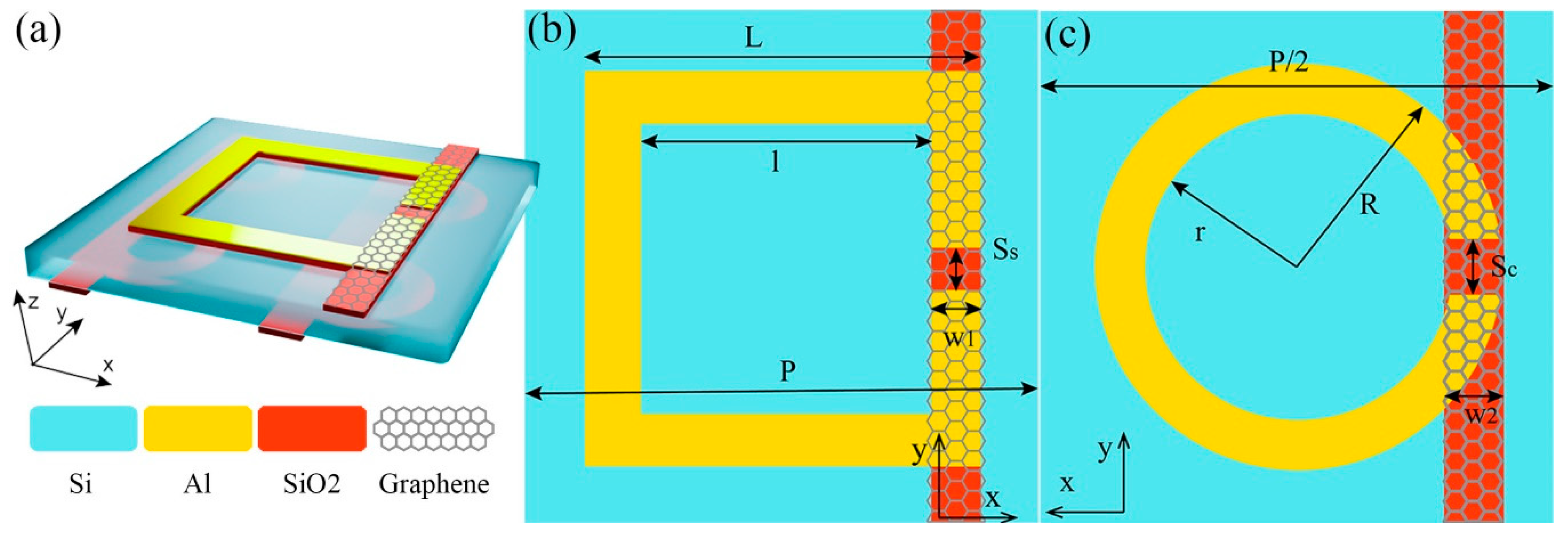
The hybrid metamaterials were made of periodic unit cells diagramed in Figure 1a. The metallic structures functioned as the electromagnetic resonators, the graphene strips linked with electrodes worked as the controller, and the silica structures sandwiched between the metallic and graphene layers were to isolate the graphene strips and the silicon substrate [14]. The metallic structures on both surfaces were SRRs, whose shapes were square split rings on the front side and circle split rings on the other side. The closed ring-shaped silica structures were underneath the metallic layer, which were attached with strips along y axis on both surfaces. The single-layer graphene strips paralleled to y axis patch on the top of the metallic and silica structures of both side metamaterials.
The key indicator for an encoder is the modulation depth. We have optimized and determined the geometrical parameters of two resonators by comparing their performance in modulation depth. As shown in Figure 1, the dimensions of our encoder were as follows: For the square split rings shown in Figure 1b, outer and inner lengths of the arms were L = 130 μm and l = 100 μm, respectively, gap of square split ring Ss = 10 μm, width of silica (graphene) strip w1 = 15 μm, and the period of unit cell P = 180 μm; for the circle split rings shown in Figure 1c, outer and inner radii of the ring were R = 39 μm and r = 32 μm, respectively, gap of circle split ring Sc = 10 μm, width of silica (graphene) strip w2 = 10 μm, and the period of unit cell P/2 = 90 μm; for all split rings, the thicknesses of the metallic layer, silica layer and substrate were 0.2 μm, 0.3 μm and 1000 μm, respectively.
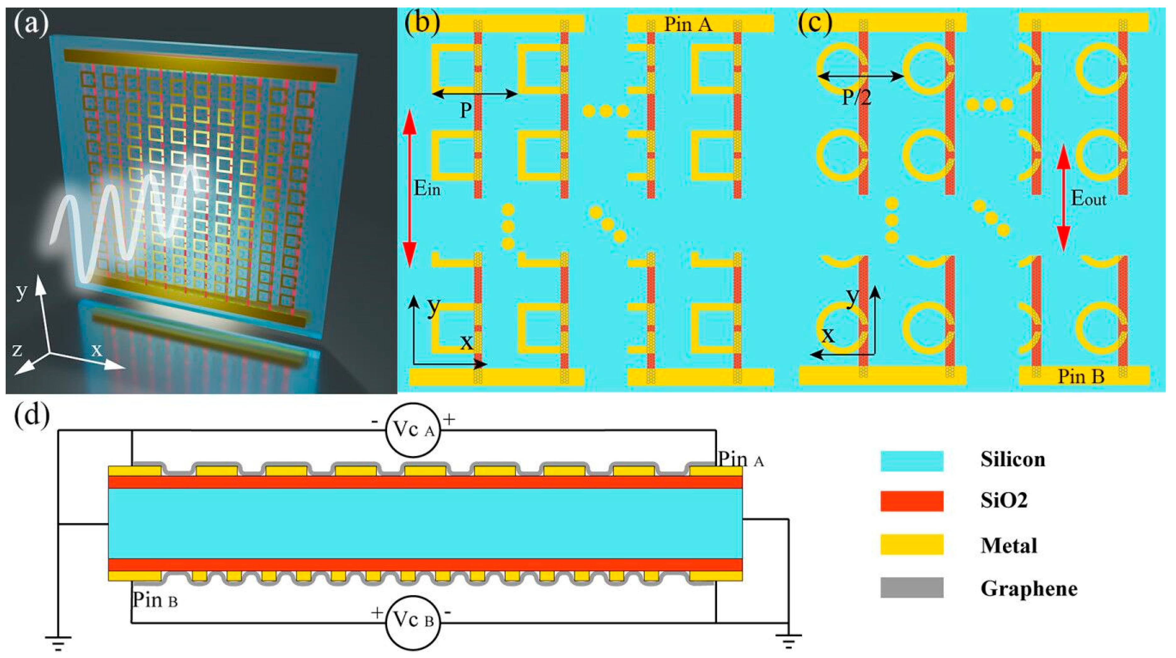
Figure 2 is the schematics of our device, which was formed of the unit cell array. We set aluminum electrodes in the edges of y axis on the front and back surfaces of the chip, which were linked to the pins of voltage control circuit PinA and PinB, respectively. The schematic of the whole device is shown in Figure 2a (note that actually the entire device has more than 50 × 50-unit cells in the xy-plane and is larger than the size of THz beam). Figure 2b,c strictly describe the structure and dimensions from the front and back views of the device, which are the period arrays of the unit cell shown in Figure 1b and 1c, respectively. As shown in Figure 2d, the metamaterials on the front and back sides were connected to the external voltage sources VCA and VCB, respectively, which could program the on–off commands independently. The separated control circuits could shift the Fermi levels of the graphene on the front and back sides individually, and therefore modulate the transmission amplitudes of dual-band determined by the double-sided metamaterials.
We simulated the transmission spectra using CST microwave studio in time domain, and the incident THz waves were polarized along the y axis. The dielectric constants of silicon and silica are 11.69 and 3.46, respectively, and the conductivity of metallic rings made of aluminum is 3.6×10⁷ S/m [25,26]. The conductivity of graphene can be expressed by the Drude-like model [27,28] , where e and are electron charge and Planck constant, respectively, and EF represents the Fermi level of graphene. The relaxation time τ can be calculated by , and in the THz regime, we set the carrier mobility μ = 3000 cm2/V∙s and the Fermi velocity vF = 1.1 × 10⁶ m/s [27,28]. Hence, the conductivity of graphene can be varied by changing the Fermi level via controlling external voltage [19,29].
Considering the manufacturing process, the chip can be feasibly fabricated by means of conventional techniques. The fabrication of the chip is divided into four steps, roughly: Firstly, grow metallic structures on the front and back surfaces of the silicon/silicon dioxide (SSD) wafer using photolithography and lift-off process [3]; secondly, the photoresist patterns and the metallic structures together serve as a mask during the reactive ion etching (RIE) of the unneeded silica structures on both sides of the SSD wafer [30]; thirdly, transfer the graphene to both sides of the chip and then pattern the graphene strips using e-beam lithography and etching with a radio frequency oxygen plasma asher [19]; finally, connect the electrodes to the external voltage source through leads [19].
3. Results and Discussion
3.1. Equivalent Circuit for the Resonators
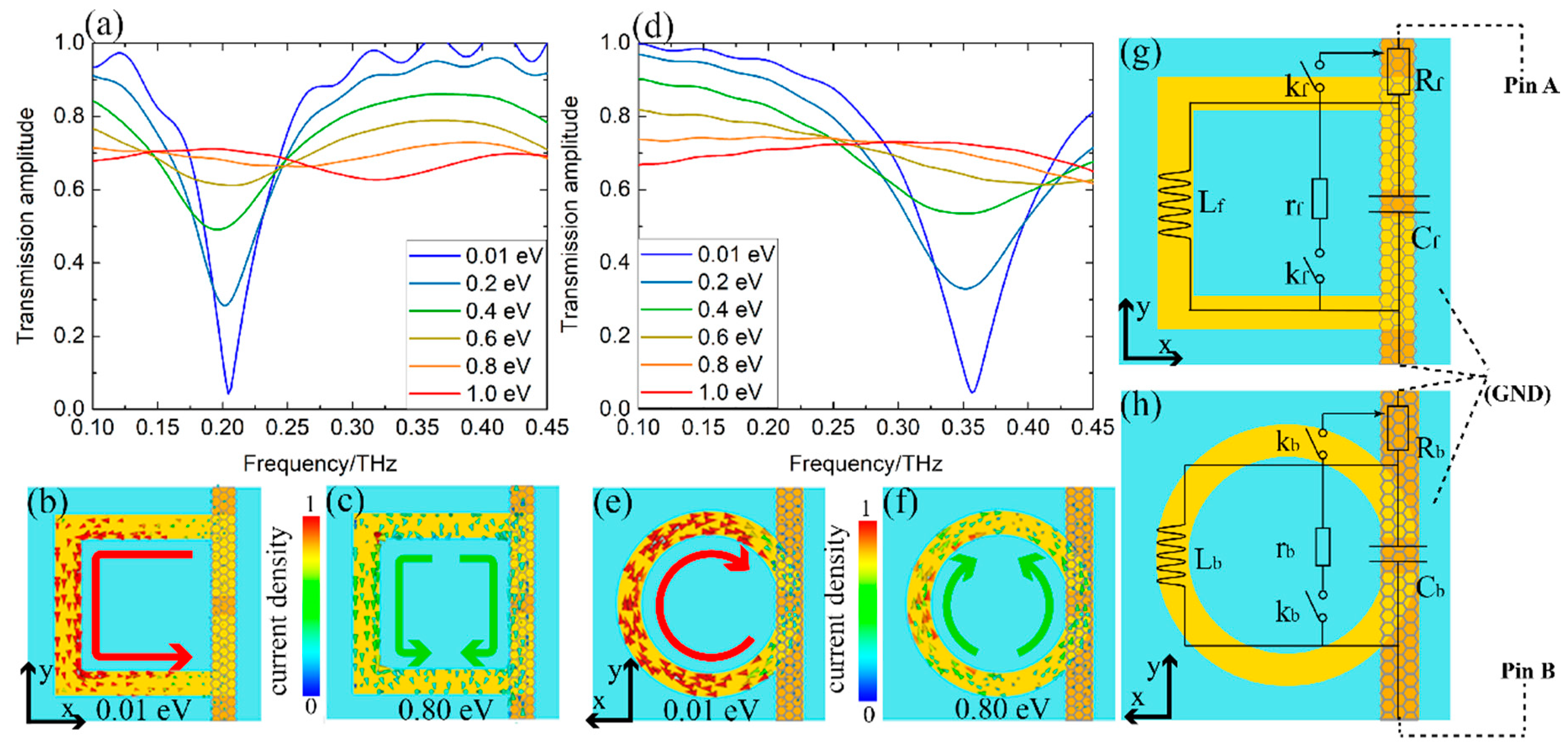
To better understand the physical mechanism affecting the performance of the encoder, we investigated the characteristics of the hybrid metamaterials on the front and back surfaces of the device separately. Figure 3a shows the normalized transmission spectra of the front side metamaterial. We simulated the results by varying the Fermi level of the graphene strips EF from 0.01 eV to 1 eV. When the EF was 0.01 eV, the resonance at 0.20 THz (band A) was obviously excited, however, as the EF increased, the resonance gradually weakened, and the bandwidth broadened. When the EF increased to 0.8 eV or higher, the resonance was almost vanished. Associated with the distributions of the surface current density in the metallic layer shown in Figure 3b,c, we can see that the loop current was evidently stimulated within the square split ring when EF = 0.01 eV; as for the case when EF = 0.8 eV, the distribution of current became symmetrical along the y axis. Similar results can be found in the transmission spectra and the distributions of the surface current density of the back-side metamaterial shown in Figure 3d–f, except that the resonance frequency was shifted to 0.33 THz (band B).
The behavior of the resonators can be explained with the theory of equivalent circuit [31,32]. For a metallic structure of split ring resonator (SRR), its gap capacitance and loop inductance can be described by an equivalent capacitance Ce and an equivalent inductance Le, respectively. In our work, when the voltage (the difference between the gate voltage and the voltage shifting the Fermi level to the Dirac point [22]) is not applied, the Fermi level of graphene is on the Dirac point. Therefore, the conductivity of graphene is very low (i.e., the graphene is hardly electrically conductive) [33]. Hence, the gap in the square/circle split ring is non-conducting. In this situation, the loop current shown in Figure 3b/e for the square/circle split ring with EF = 0.01 eV can be modeled with LC equivalent circuit, which is diagramed in Figure 3g/h, corresponding to the situation that the switch kf/b is open. Thus, the resonance frequency f of SRR can be expressed as [31,32]:
Here, the equivalent inductance Le is approximately proportional to the size of the SRR [34]. Due to the different shapes of the resonator, the size can be reasonably converted with the area. Consequently, the resonance frequency can be qualitatively estimated with fs ~ 1/L for the square split ring and fc ~ 1/R for the circle split ring. Since R is smaller than L, the resonance frequency of the circle split ring will be higher than that of the square split ring, which agrees with our results shown in Figure 3a,d. Besides, the equivalent capacitance Ce will also be affected by other parameters (gap, width or thickness of the metallic structure) [34]. As we mentioned in Section 2, we optimized the geometrical parameters of two resonators in order to obtain the good performance in modulation depth.
When the voltage is applied on the graphene strip, the Fermi level is shifted away from the Dirac point [33]. Thus, the conductivity of graphene strip becomes large, and graphene switches to be electrically conductive. Hence, the gap in the square/circle split ring is conducting to a certain extent, and the strength of the resonance will generally weaken. When the Fermi level is tuned to 0.8 eV, the equivalent circuit for the square/circle split ring, as shown in Figure 3g/h, will be altered to the RLC parallel resonance circuit, corresponding to the case that the switch kf/b is closed. Here, rf/b is the equivalent resistance between the gap and Rf/b is the equivalent resistance between the unit cells. Due to the high conductivity of graphene, the initial LC resonance is broken: each capacitator is connected in parallel with a low resistance, and the equivalent resistance between the unit cells is also reduced. As a result, the resonance behavior is changed to the symmetrical current distribution shown in Figure 3c/f, which corresponds to the dipole mode whose resonance frequency will be blue shifted. Note that if EF further rises to 1 eV, the new merged dipole mode will be resonated (obviously around 0.30 THz in Figure 3a for the square split ring) due to the metal-like conductivity of the graphene. As a result, the transmission amplitude at higher frequencies will decrease, which will make trouble for designing dual-band devices. This is why we choose 0.8 eV as the higher Fermi level corresponding to “On” status for the encoder hereinafter.
For the cases that Fermi level is between 0.01 eV and 0.8 eV, the modulation of the transmission dip also can be qualitatively explained with the theory of equivalent circuit. Take square split ring as an example: According to the relation of quality factor Q to the parameters of the equivalent circuit , when the voltage is applied, the equivalent circuit is switched from initial LC resonance circuit to RLC parallel resonance, and the parallel resistance rf varies from infinity (because of the open state of the switch kf) to a finite value. Consequently, Q will be reduced and the resonance at band A will be weakened. These coincide with the simulated results shown in Figure 3a: When Fermi level increases, the transmission gradually enlarges, and the bandwidth gradually broadens. The similar analysis also can be applied to explain the results of the circle split ring and we will not discuss in detail.
3.2. Performance of the Encoder
Now, if we choose EF = 0.01 eV as the low transmission state, and EF = 0.8 eV as the high transmission state, which corresponding to the situations without and with applying the voltage on the graphene stripes, respectively, we can obtain two different states for each resonator. In this way, we can realize one-bit coding at one band. To double the number of bits, we should assemble two resonators working at two different bands and meanwhile eliminate their coupling. We put the square and circle split ring arrays on the front and back surfaces of the metamaterials, respectively, so that the coupling between the two kinds of resonator can be effectively reduced. We have investigated the coupling effect by changing the thickness of the substrate. When the front and back side metamaterials were separated more than 500 μm, the coupling effect nearly disappeared. The reason for choosing 1 mm-thick substrate in our device is that when we detect the transmission spectrum using THz time domain system, we can get longer time signal and obtain more detailed information in the frequency domain after Fourier transform.
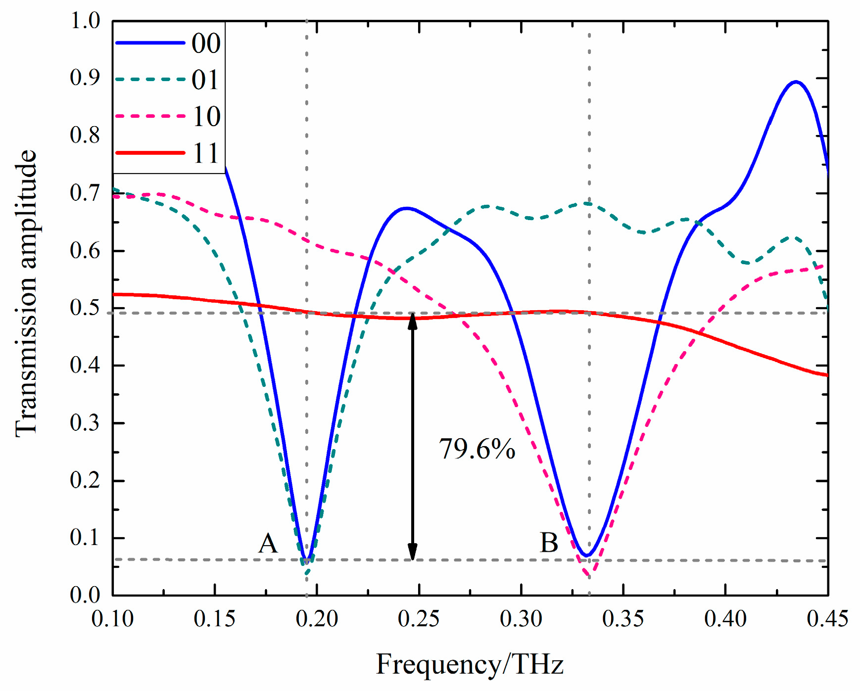
After determining the optimized geometrical parameters and Fermi level values, we simulated the performance of the encoder with double-sided hybrid metamaterials. Figure 4 demonstrates the simulated normalized transmission spectra of the device showing four encoding statuses in frequency domain, which corresponds to the different cases of the voltage control listed in Table 1. Here, for the status of the controller, “On” or “Off” refers to the situations that Pin_A/B) is loaded with or without voltages, respectively, and thus the corresponding Fermi level of the graphene is modeled as 0.01 eV or 0.8 eV, respectively; for the transmission amplitude, we define the value as “Low” or “High” depending on whether it is lower or higher than the threshold (chosen as 0.4). Apparently, we achieve four encoding statuses—00, 01, 10, 11—via modulating the transmission amplitude of bands A and B (resonated around 0.20 THz and 0.33 THz, respectively) by applying the voltages to the structures on the front and back surfaces independently. Comparing to the transmission spectra of each side metamaterials shown in Figure 3a,d, we can identify that the working bands A and B are determined by the metamaterials on the front and back surfaces, respectively. Since the frequencies of the resonance dips were barely moved, the coupling between the two metamaterials can be ignored. In order to measure the effectiveness of our device, we extracted the modulation depth from the transmission spectra (the value of modulation depth was calculated using the amplitude of codes 00 and 11). As denoted in Figure 4, the modulation depth could reach as high as 79.6%, which indicates our encoder has distinguished performance.
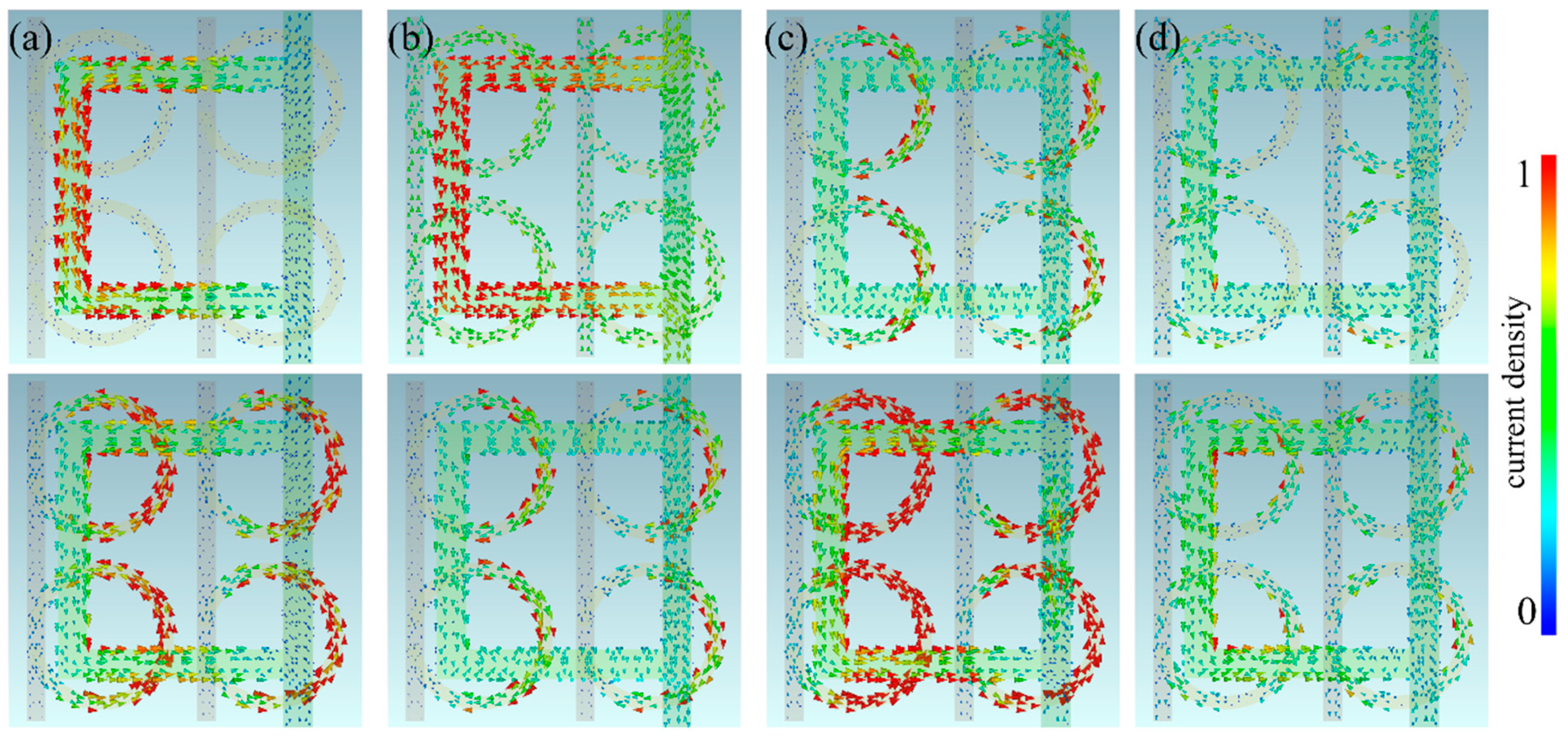
Subsequently, we investigated the resonance details about different coding states. Figure 5a–d shows the distributions of the surface current density in codes 00, 01, 10 and 11, respectively, in which the top and bottom rows correspond to the resonances at 0.20 THz (band A) and 0.33 THz (band B), respectively. Visibly, band A was dominated by the resonance in the square split rings, and band B was governed by the resonance in the circle split rings. The resonance behaviors are almost identical to those shown in Figure 3b–f. It is obvious that the resonances are strong when there is no voltage applied to the structures (for example the situation of code 00), which coincide with the deep resonance dips in the transmission spectra. If the voltage is applied to the structures (for example the situation of code 11), the resonances are much weaker, and the resonance dips will disappear in the transmission spectra.
3.3. Further Discussion
At last, we briefly discuss the issues about the potential applications. The applied voltage may be a considerable indicator for graphene-based device. According to the references [16] and [22], we can roughly estimate that the required voltage shifting Fermi level to 0.8 eV is about three hundred volt. There are two possible methods to reduce the applied voltage. One is to choose lower Fermi level as the “On” state, and the price is that the modulation depth will be diminished. The other is to decrease the thickness of silica layer, and the required voltage for the same Fermi level may be effectively reduced, but the breakdown voltage of the device will also drop off. Those solutions need more investigations based on theory and experiment, which will be the key points in our future work.
According to our simulated results and discussion, we can infer that if the metamaterials laying on different layers are distant enough, the interaction between them can be almost ignored. Thus, if we arrange more resonators by means of multiplying the layers, the functionality of the device may be efficiently expanded. Our scheme of encoder has potential in developing multibit device combined with CMOS (Complementary Metal Oxide Semiconductor) technique in the future.
4. Conclusions
We propose a two-bit encoding device working at terahertz frequencies. The device assembles the two graphene-based hybrid metamaterials with different shapes deposited on the front and back surfaces of a silicon wafer. Using the external electrodes to change the conductivities of the graphene on each side individually, we realize the active control of dual-band transmission amplitudes. The results demonstrate that our device can function at 0.20 THz and 0.33 THz with good performance, and the modulation depth can reach 79.6%. Comparing with the present THz modulators, our encoder can not only maximally enhance the coding number in a single chip, but also guarantee the modulation efficiency. The functionality of the device may also be expanded by arranging more separately controlled resonators in multilayer structures. Moreover, the device proposed in this paper can also be widely used in other bands. Our encoder may pave a new way to develop multifunctional and integrated devices, such as multiband filter and sensor, frequency division multiplexer and logical circuitry, which will promote the development of THz communications and other applications.
5. Patents
Shan Yin, Xintong Shi, Wei Huang, Ling Guo, Fangrong Hu, Wentao Zhang, Xianming Xiong. A transmission-type terahertz two-bit encoding device and system. 2019210801324 (China).
Author Contributions
Conceptualization, S.Y.; investigation and data curation, X.S.; writing—original draft preparation, S.Y., X.S. and W.H.; writing—review and editing, W.H. and W.Z.; funding acquisition, S.Y., W.H., W.Z., F.H. and Z.Q.; project administration, X.X.
Funding
This research was funded by the National Science and Technology Major Project of China (No. 2017ZX02101007-003); the National Natural Science Foundation of China (Nos. 61565004, 61665001 and 61965005); the Natural Science Foundation of Guangxi Province (Nos. 2017GXNSFBA198116 and 2018GXNSFAA281163); the Science and Technology Program of Guangxi Province (No. 2018AD19058); and the Open Project of Guangxi Colleges and Universities Key Laboratory of Complex System Optimization and Big Data Processing (No. 2017CSOBDP0203). Wei Huang acknowledges the funding from Guangxi Oversea 100 Talent Project and Wentao Zhang acknowledges the funding from Guangxi Distinguished Expert Project.
Conflicts of Interest
The authors declare no conflict of interest.
References
- Ferguson, B.; Zhang, X.C. Materials for terahertz science and technology. Nat. Mater. 2002, 1, 26. [Google Scholar] [CrossRef] [PubMed]
- Dhillon, S.S.; Vitiello, M.S.; Linfield, E.H.; Davies, A.G.; Hoffmann, M.C.; Booske, J.; Paoloni, C.; Gensch, M.; Weightman, P.; Williams, G.P.; et al. The 2017 terahertz science and technology roadmap. J. Phys. D Appl. Phys. 2017, 50, 043001. [Google Scholar] [CrossRef]
- Chen, H.-T.; O’Hara, J.F.; Azad, A.K.; Taylor, A.J.; Averitt, R.D.; Shrekenhamer, D.B.; Padilla, W.J. Experimental demonstration of frequency-agile terahertz metamaterials. Nat. Photonics 2008, 2, 295–298. [Google Scholar] [CrossRef]
- Yu, N.; Capasso, F. Flat optics with designer metasurfaces. Nat. Mater. 2014, 13, 139–150. [Google Scholar] [CrossRef] [PubMed]
- Li, C.; Chang, C.C.; Zhou, Q.; Zhang, C.; Chen, H.T. Resonance coupling and polarization conversion in terahertz metasurfaces with twisted split-ring resonator pairs. Opt. Express 2017, 25, 25842–25852. [Google Scholar] [CrossRef] [PubMed]
- Yin, S.; Hu, F.; Chen, X.; Han, J.; Chen, T.; Xiong, X.; Zhang, W. Ruler equation for precisely tailoring the resonance frequency of terahertz U-shaped metamaterials. J. Opt. 2019, 21, 025101. [Google Scholar] [CrossRef]
- Hu, F.; Guo, E.; Xu, X.; Li, P.; Xu, X.; Yin, S.; Wang, Y.; Chen, T.; Yin, X.; Zhang, W. Real-timely monitoring the interaction between bovine serum albumin and drugs in aqueous with terahertz metamaterial biosensor. Opt. Commun. 2017, 388, 62–67. [Google Scholar] [CrossRef]
- Huang, W.; Rangelov, A.A.; Kyoseva, E. Complete achromatic optical switching between two waveguides with a sign flip of the phase mismatch. Phys. Rev. A 2014, 90, 053837. [Google Scholar] [CrossRef] [Green Version]
- Chen, X.; Ghosh, S.; Xu, Q.; Ouyang, C.; Li, Y.; Zhang, X.; Tian, Z.; Gu, J.; Liu, L.; Azad, A.K.; et al. Active control of polarization-dependent near-field coupling in hybrid metasurfaces. Appl. Phys. Lett. 2018, 113, 061111. [Google Scholar] [CrossRef]
- Chen, H.-T.; Padilla, W.J.; Cich, M.J.; Azad, A.K.; Averitt, R.D.; Taylor, A.J. A metamaterial solid-state terahertz phase modulator. Nat. Photonics 2009, 3, 148–151. [Google Scholar] [CrossRef]
- Li, H.; Cao, Q.; Liu, L.; Wang, Y. An Improved Multifunctional Active Frequency Selective Surface. IEEE Trans. Antennas Propag. 2018, 66, 1854–1862. [Google Scholar] [CrossRef]
- Wang, L.; Zhang, Y.; Guo, X.; Chen, T.; Liang, H.; Hao, X.; Hou, X.; Kou, W.; Zhao, Y.; Zhou, T.; et al. A Review of THz Modulators with Dynamic Tunable Metasurfaces. Nanomaterials 2019, 9, 965. [Google Scholar] [CrossRef] [PubMed] [Green Version]
- Jnawali, G.; Rao, Y.; Yan, H.; Heinz, T.F. Observation of a transient decrease in terahertz conductivity of single-layer graphene induced by ultrafast optical excitation. Nano Lett. 2013, 13, 524–530. [Google Scholar] [CrossRef] [PubMed]
- Yin, Y.; Cheng, Z.; Wang, L.; Jin, K.; Wang, W. Graphene, a material for high temperature devices--intrinsic carrier density, carrier drift velocity, and lattice energy. Sci. Rep. 2014, 4, 5758. [Google Scholar] [CrossRef] [PubMed] [Green Version]
- Huang, W.; Liang, S.-J.; Kyoseva, E.; Ang, L.K. Adiabatic control of surface plasmon-polaritons in a 3-layers graphene curved configuration. Carbon 2018, 127, 187–192. [Google Scholar] [CrossRef] [Green Version]
- Dabidian, N.; Kholmanov, I.; Khanikaev, A.B.; Tatar, K.; Trendafilov, S.; Mousavi, S.H.; Magnuson, C.; Ruoff, R.S.; Shvets, G. Electrical Switching of Infrared Light Using Graphene Integration with Plasmonic Fano Resonant Metasurfaces. ACS Photonics 2015, 2, 216–227. [Google Scholar] [CrossRef]
- Farmer, D.B.; Avouris, P.; Li, Y.; Heinz, T.F.; Han, S.J. Ultrasensitive Plasmonic Detection of Molecules with Graphene. ACS Photonics 2016, 3, 553–557. [Google Scholar] [CrossRef]
- Li, Q.; Tian, Z.; Zhang, X.; Singh, R.; Du, L.; Gu, J.; Han, J.; Zhang, W. Active graphene-silicon hybrid diode for terahertz waves. Nat. Commun. 2015, 6, 7082. [Google Scholar] [CrossRef]
- Kindness, S.J.; Almond, N.W.; Wei, B.; Wallis, R.; Michailow, W.; Kamboj, V.S.; Braeuninger-Weimer, P.; Hofmann, S.; Beere, H.E.; Ritchie, D.A.; et al. Active Control of Electromagnetically Induced Transparency in a Terahertz Metamaterial Array with Graphene for Continuous Resonance Frequency Tuning. Adv. Opt. Mater. 2018, 6, 1800570. [Google Scholar] [CrossRef] [Green Version]
- Kleine-Ostmann, T.; Nagatsuma, T. A Review on Terahertz Communications Research. J. Infrared Millim. Terahertz Waves 2011, 32, 143–171. [Google Scholar] [CrossRef]
- Naeem, N.; Parveen, S.; Ismail, A. Terahertz Communications for 5G and Beyond. In Antenna Fundamentals for Legacy Mobile Applications and Beyond; Elfergani, I., Hussaini, A.S., Rodriguez, J., Abd-Alhameed, R., Eds.; Springer International Publishing: Cham, Switzerland, 2018; pp. 305–322. [Google Scholar]
- Gao, W.; Shu, J.; Reichel, K.; Nickel, D.V.; He, X.; Shi, G.; Vajtai, R.; Ajayan, P.M.; Kono, J.; Mittleman, D.M.; et al. High-Contrast Terahertz Wave Modulation by Gated Graphene Enhanced by Extraordinary Transmission through Ring Apertures. Nano Lett. 2014, 14, 1242–1248. [Google Scholar] [CrossRef] [PubMed]
- Fan, Y.; Qian, Y.; Yin, S.; Li, D.; Jiang, M.; Lin, X.; Hu, F. Multi-band tunable terahertz bandpass filter based on vanadium dioxide hybrid metamaterial. Mater. Res. Express 2019, 6, 055809. [Google Scholar] [CrossRef]
- Xiao, S.; Wang, T.; Liu, T.; Yan, X.; Li, Z.; Xu, C. Active modulation of electromagnetically induced transparency analogue in terahertz hybrid metal-graphene metamaterials. Carbon 2018, 126, 271–278. [Google Scholar] [CrossRef] [Green Version]
- Srivastava, Y.K.; Manjappa, M.; Cong, L.; Cao, W.; Al-Naib, I.; Zhang, W.; Singh, R. Ultrahigh-Q Fano Resonances in Terahertz Metasurfaces: Strong Influence of Metallic Conductivity at Extremely Low Asymmetry. Adv. Opt. Mater. 2015, 4, 457–463. [Google Scholar] [CrossRef]
- Ordal, M.A.; Long, L.L.; Bell, R.J.; Bell, S.E.; Bell, R.R.; Alexander, R.W.; Ward, C.A. Optical properties of the metals Al, Co, Cu, Au, Fe, Pb, Ni, Pd, Pt, Ag, Ti, and W in the infrared and far infrared. Appl. Opt. 1983, 22, 1099–1120. [Google Scholar] [CrossRef]
- Liu, T.; Zhou, C.; Cheng, L.; Jiang, X.; Wang, G.; Xu, C.; Xiao, S. Actively tunable slow light in a terahertz hybrid metal-graphene metamaterial. J. Opt. 2019, 21, 035101. [Google Scholar] [CrossRef] [Green Version]
- Wang, X.; Meng, H.; Deng, S.; Lao, C.; Wei, Z.; Wang, F.; Tan, C.; Huang, X. Hybrid Metal Graphene-Based Tunable Plasmon-Induced Transparency in Terahertz Metasurface. Nanomaterials 2019, 9, 385. [Google Scholar] [CrossRef] [Green Version]
- Gomez-Diaz, J.S.; Moldovan, C.; Capdevila, S.; Romeu, J.; Bernard, L.S.; Magrez, A.; Ionescu, A.M.; Perruisseau-Carrier, J. Self-biased reconfigurable graphene stacks for terahertz plasmonics. Nat. Commun. 2015, 6, 6334. [Google Scholar] [CrossRef]
- Gaboriau, F.; Cartry, G.; Peignon, M.C.; Cardinaud, C. Selective and deep plasma etching of SiO2: Comparison between different fluorocarbon gases (CF4, C2F6, CHF3) mixed with CH4 or H2 and influence of the residence time. J. Vac. Sci. Technol. B Microelectron. Nanometer Struct. 2002, 20, 1514. [Google Scholar] [CrossRef]
- Shamonin, M.; Shamonina, E.; Kalinin, V.; Solymar, L. Properties of a metamaterial element: Analytical solutions and numerical simulations for a singly split double ring. J. Appl. Phys. 2004, 95, 3778–3784. [Google Scholar] [CrossRef]
- Shelton, D.J.; Brener, I.; Ginn, J.C.; Sinclair, M.B.; Peters, D.W.; Coffey, K.R.; Boreman, G.D. Strong coupling between nanoscale metamaterials and phonons. Nano Lett. 2011, 11, 2104–2108. [Google Scholar] [CrossRef] [PubMed]
- Novoselov, K.S.; Geim, A.K.; Morozov, S.V.; Jiang, D.; Zhang, Y.; Dubonos, S.V.; Grigorieva, I.V.; Firsov, A.A. Electric Field Effect in Atomically Thin Carbon Films. Science 2004, 306, 666–669. [Google Scholar] [CrossRef] [PubMed] [Green Version]
- Qun, W.; Ming-Feng, W.; Fan-Yi, M.; Jian, W.; Le-Wei, L. Modeling the effects of an individual SRR by equivalent circuit method. In Proceedings of the 2005 IEEE Antennas and Propagation Society International Symposium, Washington, DC, USA, 3–8 July 2005; pp. 631–634. [Google Scholar]
Figure 1.
Structures of the unit cell: (a) The schematic of the unit cell, (b) the front and (c) the back views of the unit cell.
Figure 1.
Structures of the unit cell: (a) The schematic of the unit cell, (b) the front and (c) the back views of the unit cell.

Figure 2.
Structures of the device: (a) The schematic of the device; (b) the front view, (c) back view and (d) lateral view of the device.
Figure 2.
Structures of the device: (a) The schematic of the device; (b) the front view, (c) back view and (d) lateral view of the device.

Figure 3.
(a) Transmission spectra, distributions of the surface current density with (b) EF = 0.01 eV and (c) EF = 0.8 eV of the single metamaterial on the front surface. (d) Transmission spectra, distributions of the surface current density with (e) EF = 0.01 eV and (f) EF = 0.8 eV of the single metamaterial on the back surfaces. Equivalent circuit diagrams of the resonator in the (g) front and (h) back-side metamaterials.

Figure 4.
Normalized transmission of the device in different encoding cases.

Figure 5.
Distributions of surface current density in different codes at 0.20 THz (top row) and 0.33 THz (bottom row): (a) code 00, (b) code 01, (c) code 10, (d) code 11.
Figure 5.
Distributions of surface current density in different codes at 0.20 THz (top row) and 0.33 THz (bottom row): (a) code 00, (b) code 01, (c) code 10, (d) code 11.


Table 1.
Encoding status and the corresponding status of the controller and the transmission.
| Code | Voltage of Controller | Transmission Amplitude | ||
|---|---|---|---|---|
| Pin_A | Pin_B | Band A | Band B | |
| 00 | Off 1 | Off | Low | Low |
| 01 | Off | On | Low | High |
| 10 | On 2 | Off | High | Low |
| 11 | On | On | High | High |
1 Status “Off” was simulated with EF = 0.01 eV. 2 Status “On” was simulated with EF = 0.8 eV.
© 2019 by the authors. Licensee MDPI, Basel, Switzerland. This article is an open access article distributed under the terms and conditions of the Creative Commons Attribution (CC BY) license (http://creativecommons.org/licenses/by/4.0/).
Share and Cite
MDPI and ACS Style
Yin, S.; Shi, X.; Huang, W.; Zhang, W.; Hu, F.; Qin, Z.; Xiong, X. Two-Bit Terahertz Encoder Realized by Graphene-Based Metamaterials. Electronics 2019, 8, 1528. https://doi.org/10.3390/electronics8121528
AMA Style
Yin S, Shi X, Huang W, Zhang W, Hu F, Qin Z, Xiong X. Two-Bit Terahertz Encoder Realized by Graphene-Based Metamaterials. Electronics. 2019; 8(12):1528. https://doi.org/10.3390/electronics8121528
Chicago/Turabian StyleYin, Shan, Xintong Shi, Wei Huang, Wentao Zhang, Fangrong Hu, Zujun Qin, and Xianming Xiong. 2019. "Two-Bit Terahertz Encoder Realized by Graphene-Based Metamaterials" Electronics 8, no. 12: 1528. https://doi.org/10.3390/electronics8121528
Note that from the first issue of 2016, this journal uses article numbers instead of page numbers. See further details here.