Analysis of DC Link Energy Storage for Single-Phase Grid-Connected PV Inverters


1
School of Electrical & Electronic Engineering, Bilecik Seyh Edebali University, Bilecik 11230, Turkey
2
Barbara Hardy Institute, University of South Australia, Adelaide 5095, Australia
3
School of Electrical & Electronic Engineering, University of Adelaide, Adelaide 5005, Australia
*
Author to whom correspondence should be addressed.
Electronics 2019, 8(6), 601; https://doi.org/10.3390/electronics8060601
Submission received: 16 April 2019
/
Revised: 23 May 2019
/
Accepted: 24 May 2019
/
Published: 29 May 2019
(This article belongs to the Special Issue Grid Connected Photovoltaic Systems)
Abstract
:Single-phase grid-connected photovoltaic (PV) inverters (GCI) are commonly used to feed power back to the utility. However, the inverter output power fluctuates at 100 Hz, which can be seen by the PV panel, and this reduces the PV output power. It is important to determine and analyze the correlation between the array voltage and current ripple and the average output power reduction of PV array. Therefore, this paper investigates the relationships between the oscillations due to single-phase switching and the DC link energy storage for PV GCIs. The balanced ripple definition is introduced and compared with the more common centered ripple definition. Some examples are provided that demonstrate the importance of these results, in the inverter design industry. The analysis presented here incorporates inductor trade-offs, which are verified with experimental results.
1. Introduction
Environmental challenges, such as climate change and pollution, increase the motivation to utilize more renewable energy sources. Solar energy is clean and cost-effective yet requires a grid-connected photovoltaic (PV) inverter (GCI) to feed the DC power into the AC network.
Generally, low power applications (<10 kW) use a single-phase AC grid connection. The instantaneous power waveform of the GCI fluctuates at twice the network frequency, e.g., at 100 Hz in Australia. Such a power fluctuation can reduce the output power of the PV panel if the inverter does not utilize energy storage. As such, energy storage components are utilized, after the PV array, to minimize the power fluctuations and hence PV output power loss.
1.1. GCI Topologies
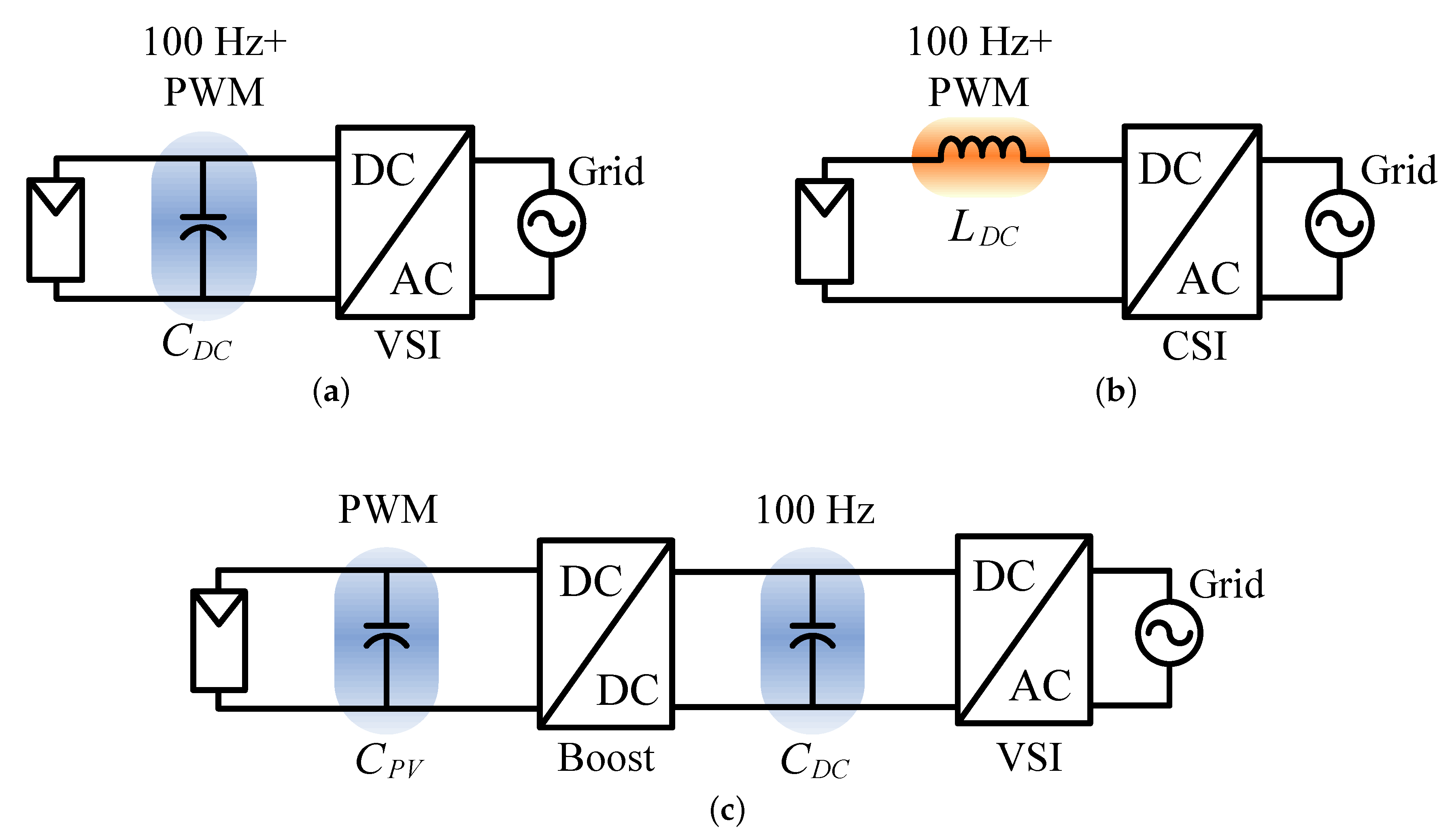
A GCI can be categorized as a voltage-source inverter (VSI) if there is a parallel capacitor at the DC link, or as a current-source inverter (CSI) if there is a series inductor at the DC link after a power source. Figure 1a,b show these single-stage CSI and VSI topologies [1], respectively, whilst Figure 1c shows a two-stage inverter topology where each capacitor minimizes losses at different frequencies. An energy storage element is required to reduce losses at double the line (network) and pulse width modulation (PWM) frequencies.
Minimizing the size of the required DC link energy storage component is critical, as this attracts cost, weight, size, and reliability (especially for electrolytic capacitors) of the storage element and the inverter. Some limitations on the minimum amount of DC link energy storage include:
- the maximum permissible PV array output current or voltage ripple to maintain the average PV array output power reduction within acceptable limits, and
- the highest permissible inverter input current ripple (for a CSI) or voltage ripple (for a VSI) before higher levels of harmonic content (in the output current of the inverter) are fed into the grid.
A converter with two stages, i.e., a DC-DC and then a DC-AC converter can separate above limitations. The first part isolates between the PV array and the 100 Hz fluctuations (see Figure 1c), whilst the PV capacitor () is required only to filter out power fluctuations due to PWM switching. This first-stage also achieves maximum power point tracking (MPPT). The capacitor () of Figure 1a must provide energy storage to limit the maximum allowable inverter input ripple, which can adversely effect the PV array output power. On the other hand, the two-stage topology (Figure 1c) has drawbacks, such as: degraded reliability and efficiency, control complexity, and higher cost; the latter is due to the increased number of stages and electronic components.
1.2. Energy Storage in Single-Phase CSI
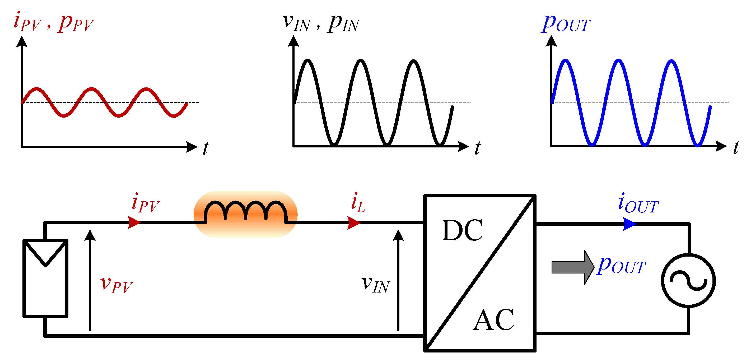
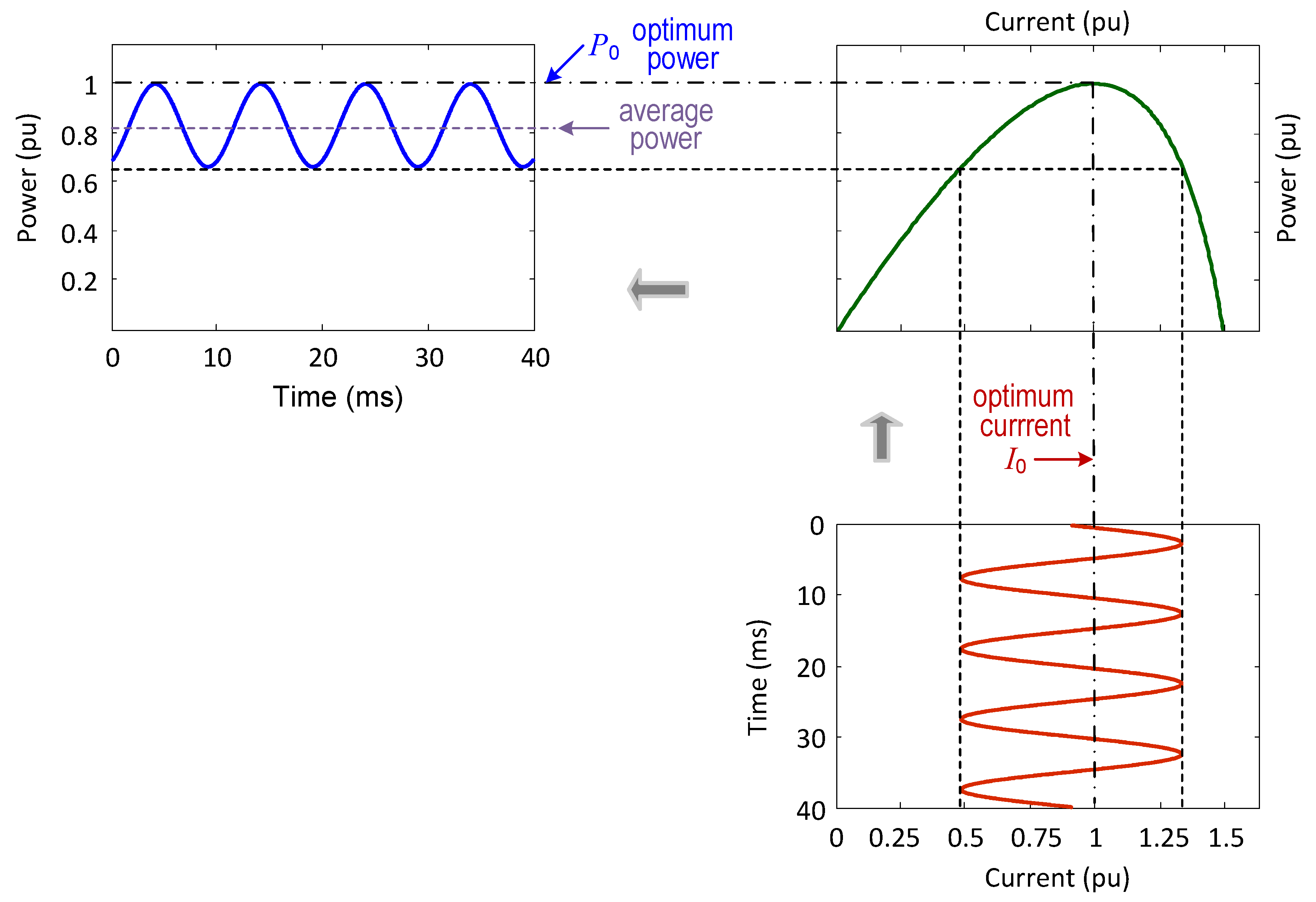
The main objective of a current-source GCI is to convert DC power generated by PV modules into grid-synchronized AC power at unity power-factor. The instantaneous output power of the inverter has a magnitude of twice the average output power, as well as twice the line frequency, as illustrated in Figure 2. Since the inverter does not contain energy storage components, its instantaneous input power should match the output power, assuming an ideal (lossless) inverter. Therefore, an energy storage inductor is realized after the PV modules to reduce the instantaneous power variations, which are seen across the PV modules. The dashed line represents the average power synchronized with the grid and the average PV array output power.
The energy stored by the inductor is proportional to current squared. Power variations will influence the amount of energy stored in the inductor, and hence cause the inductor current and PV array output voltage to vary. Figure 3 shows that the current change leads a loss in the PV array average output power even though the average value of the PV output current may still be the current corresponding to the maximum power point (MPP), (). This stems from the PV output power, which is only maximum when the current is at , hence when the output current varies from its ideal value, the available output power is always reduced. For this reason, this study focused on the effect of the energy storage component on the voltage and current waveforms; these were systematically examined to estimate the reduction of PV array power.
1.3. Literature Review
The reduction of the average output power indicates that the amount of ripple in the current or voltage increases. Although the average power reduction of PV arrays based on output current or voltage ripple is well-known and considered in practical designs, more analysis of the effect is required. Kjaer [2] studied the voltage ripple effect on a single-stage VSI for both cadmium telluride (CdTe) and standard silicon PV modules. It is assumed that the sinusoidal voltage ripple is centered at the optimum voltage. The presented theoretical model was the PV array voltage curve, which varies around the MPP and used Taylor’s theorem to estimate a permissible ripple voltage for average power reductions range from 0.1% to 2%. He also analyzed the connection between capacitor size and voltage fluctuation due to instantaneous power ripple (100 Hz). Accordingly, he defines the correlation between the smallest appropriate capacitor size (in parallel with the PV array) and the PV array specifications and the reasonable average power reduction level.
Casadei et al. [3] employed the double-frequency voltage and current fluctuations as perturbation components for MPPT. They stated that the voltage ripple was a function of average output power, , angular frequency of grid, , and capacitance in the DC link, , as shown in Equation (1):
The same equation was used to calculate the required capacitance for the DC link capacitors in [4,5,6,7,8]. Currently, some research has been done regarding VSIs, for instance, a model was demonstrated for determining the power reduction in the PV array related to the switching frequency of boost converters [9] and was used to design a reconfigurable DC link inductor. A PV array power reduction assumption has been examined for partial shading conditions based on the rms ripple voltage [10]. It was shown that the power reduction can be significant.
Bush and Wang [11] reported an interesting single-phase CSI topology that used six IGBTs and series diodes similar to three-phase CSIs. The inductor at the DC link was downsized by controlling the switches using space-vector modulation. A similar study was undertaken with a different control approach to reduce the DC link capacitor size [12]. The ripple confinement feedback control was used to control two equal capacitor voltages at the AC side without any energy storage component. An interesting modulation approach for a CSI topology was reported in [13] to reduce energy storage requirement at the DC link. Some control techniques oriented studies were reported, such as predictive DC voltage control and bus control [14,15], in order to reduce DC link energy storage component. A common two stage inverter used an extra ripple circuit module, which allows using film capacitors with less energy storage capacity compared to electrolytic capacitors [16]. Other means were reported in the literature to decrease the DC link capacitor or inductor sizes [17,18,19,20,21,22,23,24,25,26,27]. These topologies include extra circuitry, such as switching and passive components in the main current path. The higher number of components resulted in complex control, additional losses, and reliability concerns. The authors have also done some work to investigate the current ripple effect in a current-source inverter employing an expression similar to Equation (1) [28,29]. The original contribution of this study is to provide physical insights into the issue of average power reduction of PV arrays by:
- investigating higher magnitude current or voltage ripple where the Taylor series approximation and assumption that the ripple is centered on the optimum current or voltage does not hold,
- introducing a parameter named the normalized energy ripple to relate the current and voltage ripple with the capacity of necessary energy storage,
- expanding the arguments to CSIs by designing an optimized DC link energy storage inductor,
- investigating the impact of temperature and irradiance variations on the results, and
- investigating the correlation between the inductor size and the average power reduction.
The paper has the following structure: Section 2 examines the impact of the current and voltage fluctuation on the average PV array output power, Section 3 discusses the link between the current and the amount of energy storage and voltage ripple, and Section 4 describes design and analysis of a particular inductor, whilst Section 5 shows experimental results. Finally, Section 6 discusses the conclusions of this study.
2. Impact of Ripple on Average PV Array Output Power
This section examines the behavior of the average PV array output power as a function of array output voltage and current ripple. The shape of the current-voltage curve indicates that the basic shape characteristics are unaffected by irradiance and temperature changes. Therefore, knowing the voltage or current ripple value is enough to calculate the average output power loss expected.
2.1. Temperature and Irradiance Curves with Normalizations
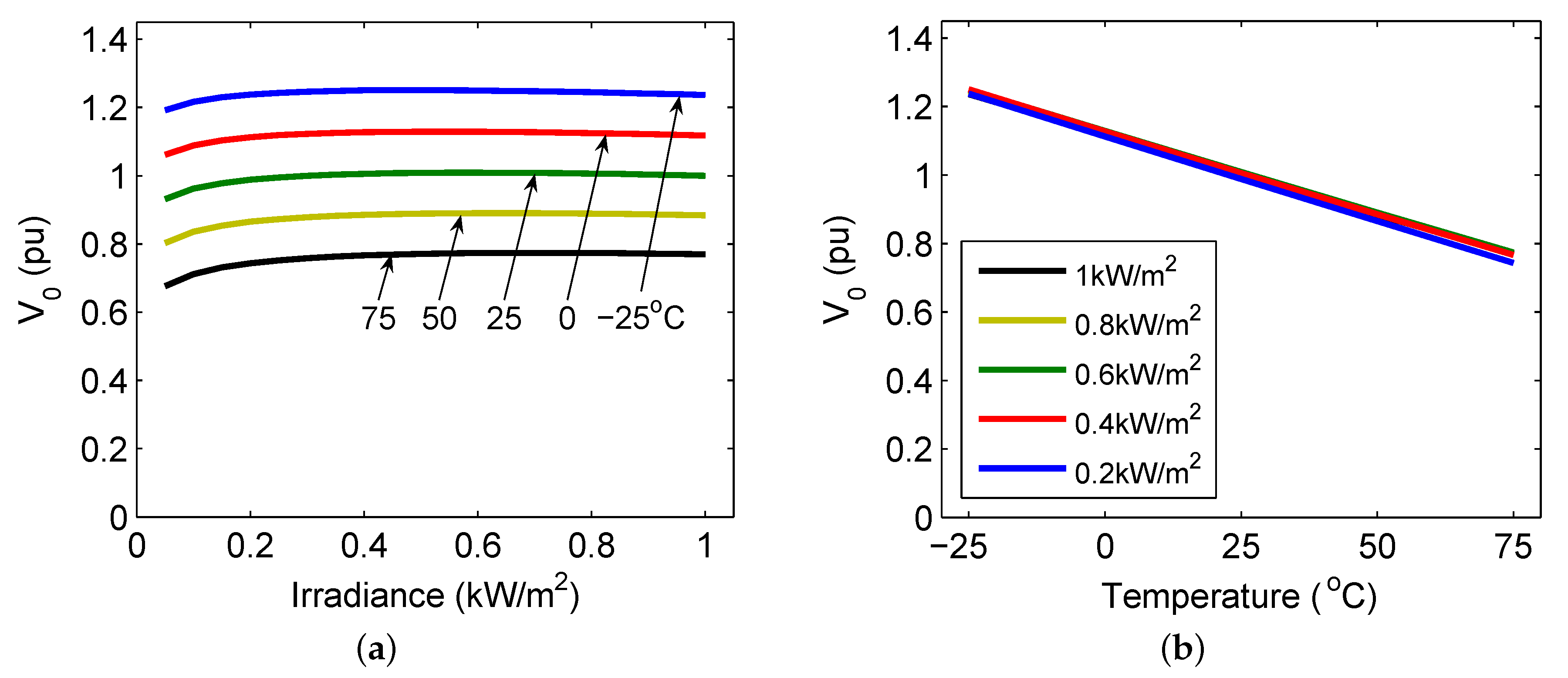
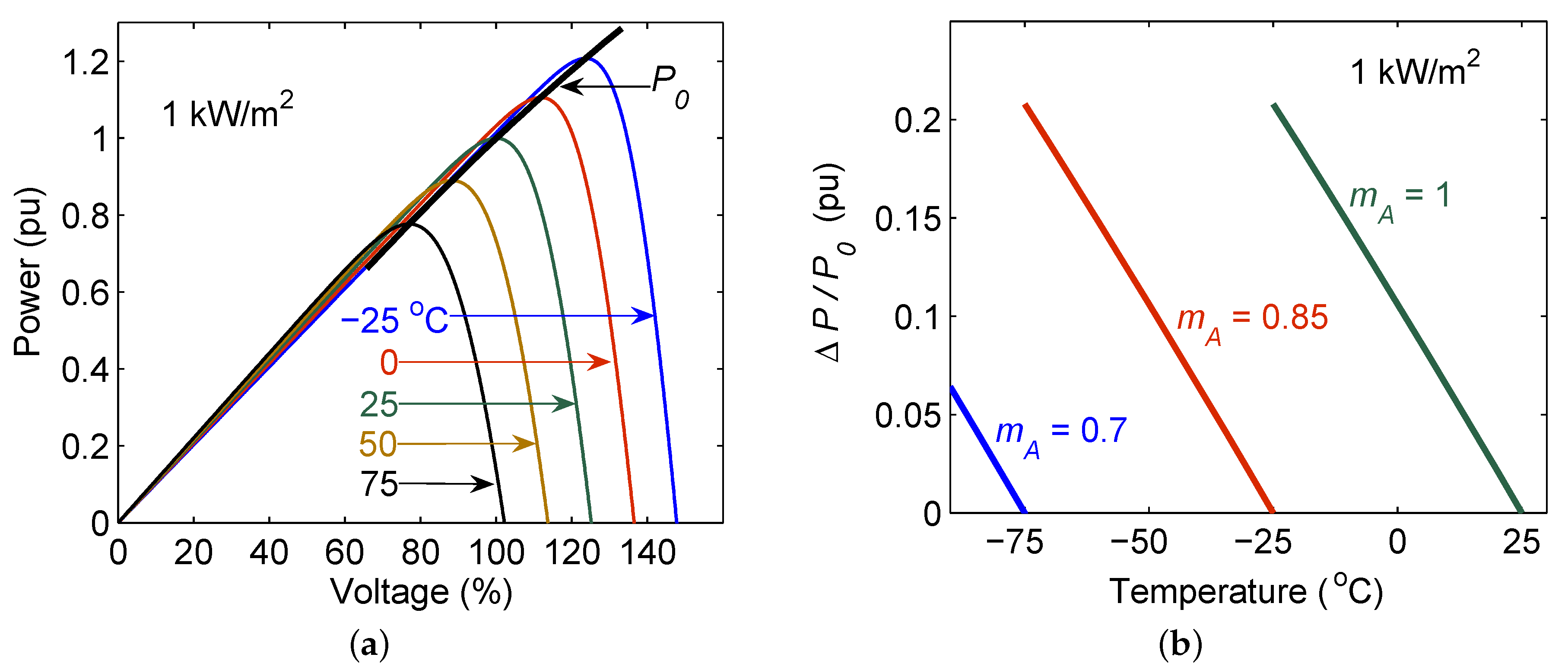
Table 1 shows the non-linear model estimations for the BP380 current-voltage and power-voltage loci for temperature and irradiance changes. The first row of the table is given to show the actual values obtained from modeling datasheet parameters and experimentally verified; dots indicate the maximum power points. The second row shows the normalized equivalents of the first row based on the MPP under nominal conditions (irradiation of 1000 W/m, 25 C), whilst the last row shows normalized curves for all MPPs. The impact of solar irradiance and temperature fluctuation on the module’s output voltage corresponding to MPP, is presented in Figure 4. Figure 4a demonstrates the impact of irradiance. Figure 4b shows a significant decrease of with temperature, as the voltage stays relatively constant except at low irradiation values.
A voltage difference of 0.37 pu exists between temperature values of 25 and 75 C, according to the normalized I-V curve in Table 1, which significantly affects the output power (almost 35%). In order for the grid-connected CSI to operate in an optimal way, it is required to select the suitable ratio between the nominal PV array voltage and the peak grid voltage. The inverter is controlled by adjusting the modulation index (). This is the ratio of peak value of the reference sinewave to the peak value of the carrier signal. It can be used to determine the amplitude of the fundamental output voltage, however, here the determines the rms amplitude of the output current, as a ratio of the maximum rms output current capability of the inverter. The MPP tracker ensures the system operates at the maximum output power point by continuously varying the inverter modulation index, as the temperature and/or irradiance change. The inverter is designed such that the optimal value of remains less than unity at the highest expected operating temperature. The third row of Table 1 illustrates the normalized curves based on respective condition MPP values. Note that the maximum power point is the same for each curve, which is independently normalized, and that the shape of I-V and P-V loci are not dependent on temperature and irradiance. The characteristics of these normalization curves are used to determine the reduction in average PV panel output power, given the inverter studied here has a single-phase output.
2.2. Average Output Power Reduction Due to Ripple
Two different definitions of the (peak-to-peak) voltage ripple are presented in Figure 5. According to Kjaer [2], this must be “centered” on the MPP voltage , and for this, a second-order Taylor polynomial was employed for the PV cells P-V characteristics. The previously mentioned method gives adequate results for low values of voltage ripple (see Figure 5a). Meanwhile, Figure 5b presents a P-V locus for larger voltage ripple values. This is based on a “balanced” definition, where the output power is made equal at the voltage extremes, and, therefore, a maximum output power will be normally provided and the actual operating point produced by an MPPT algorithm will be more accurately represented (see Figure 6). The same definitions are applied to the current ripple .
The average power loss related to the voltage or current ripple calculated with the normalized power-current and power-voltage curves, as well as the ripple definitions under standard conditions, are presented in Figure 6. As previously shown in Figure 3, it presumes a sinusoidal current or voltage ripple with time-varying amplitude, as a result of the instantaneous output power waveform. This allows the average output power reduction to be calculated.
The power reduction at a given level of current or voltage ripple is similar for the balanced definition, whilst the power losses are higher using the centered definition; the latter is particularly noticeable for the current ripple.
Note that for small values of ripple (<7.5%), the power losses are similar regardless of the definition used, however, as the ripple increases, the power loss increases using the centered current definition. For instance, a 12% current ripple results in a 1.3% and 2.1% power reduction using the balanced and centered definitions.
The red circles of Figure 6 represent results calculated from [2], by means of a second-order Taylor polynomial for the P-V curve for a silicon PV array using the centered ripple definition. These results, from [2] match the estimated curve at low ripple values (<7.5%), however, they are lower power losses at higher levels of current or voltage ripple.
3. Effect of Energy Storage on Current/Voltage
Figure 2 illustrates a single-stage current-source design with a bulky DC link inductor, where the single-phase inverter instantaneous output power (t) has fluctuations at twice the line frequency. Assuming the inductor current (t) is effectively constant, Equation (2) presents the input voltage of the inverter (t).
As shown in Figure 2, it is initially assumed that the PV output voltage is essentially constant. Moreover, it is assumed to have a value which is equal to the average value of (t), since the inductor behaves as a short-circuit to DC. As it was initially assumed that (t) and are constant, the PV array output power is also considered to be constant. Nevertheless, the inverter’s instantaneous input power is time-varying. Therefore, the power difference between the amount provided by the solar cell and the amount required by the inverter should be supplied and absorbed by the inductor. The energy which is stored in the DC link inductor has an average value of and a ripple of and changes in proportion to the current. Therefore, with the absorption and release of the energy, the inductor current (t) must vary in the course of the cycle. As the DC link inductor voltage corresponds to the difference between the PV array voltage and the inverter input voltage , that is, a sinewave with a mean value of zero. Subsequently, the DC link inductor current is represented by a cosine waveform with an offset that is equal to the average PV array current. Therefore, it is reasonable to have a rough correlation between the current ripple and the size of the inductor at the DC link.
Equation (3) represents the average stored energy in the DC link inductor:
Equation (4) expresses the inductor energy ripple :
where is the DC voltage at the MPP, is the grid voltage angular frequency, and T is the period of the instantaneous power waveform (twice the grid frequency). The current ripple is associated with the energy ripple for small ripple magnitudes, as shown in Equation (5):
This is similarly shown for a VSI, which has a capacitor at the DC link, as shown in Equation (7):
These equations provide a straightforward connection between the voltage (and equivalent current) ripple, the energy ripple (determined by the grid frequency and output power (Equation (5)), and the stored energy [28].
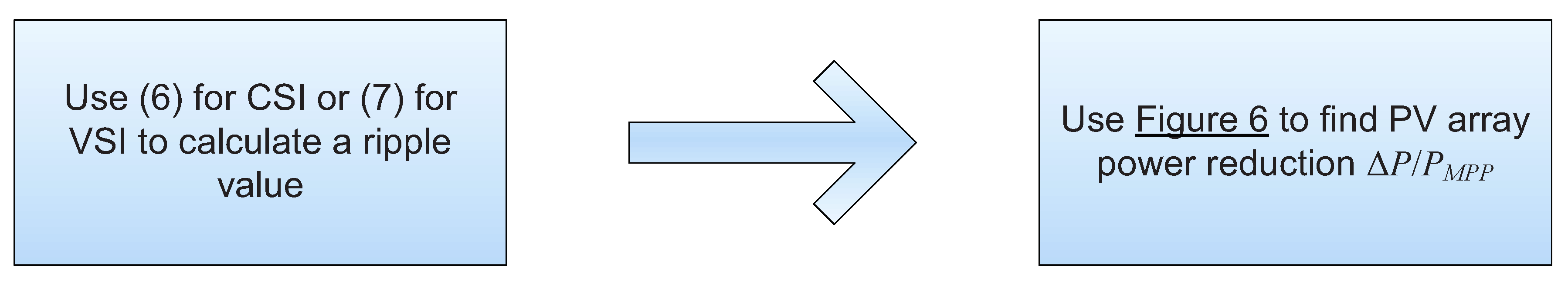
Application Examples
Figure 7 shows a block diagram to calculate the reduction of PV array output power. Firstly, the peak-to-peak current (for CSI) or voltage (for VSI) ripple values are computed using Equations (6) and (7), respectively. The resulting reduction of PV array output power / is predicted using the balanced definition seen in Figure 6.
Table 2 compares four different GCIs, i.e., two VSI and two CSI designs. It shows data, such as the rated PV output power, grid frequency, voltage and current at the MPP, DC link capacitances, DC link inductances, energy storage values (mJ/W), power reduction of PV cells, and energy storage element resistive losses.
As previously indicated, the peak-to-peak low ripple is less than 7.5% whilst the high ripple is more than 10%. This can also be seen in Figure 6. From Table 2 both VSI designs have low power ripples, i.e., 4.3% and 2.8%. However, both CSI designs are more on the high side, i.e., 7.1% and 10.6%, although they have large DC link inductors. Please note that no international standards exist yet regarding 100 Hz fluctuations at the DC link, however, it is industry practice to limit the ripple to 5% for a single-phase, and 3% for a three-phase GCI. Nevertheless, there could be more or less ripple preferences based on the control scheme and MPP tracking accuracy.
Table 2 shows the average PV array power reduction of total power losses of <0.2% for both VSI designs. The VSI designs use low-cost DC link capacitors which attract negligible losses, unlike the first CSI which, according to [32], has 16% copper losses due to the DC link inductor resistance. This copper loss is an important issue regarding the effectiveness of the CSIs; a physically smaller DC link inductor could be used to significantly reduce inductor losses. However, the reduction in PV array output power increases as the inductor size decreases. Comparatively high inductances are used in both CSI designs, and, therefore, a large DC link inductor is needed (see Table 3).
Nevertheless, the DC link inductors of both CSIs store less energy than the DC link capacitors of both VSIs. As such, the reduction of PV array average power and inductor size analyses should be carried out using the balanced definition. The equivalent series resistance (ESR) values for the DC link capacitors are acquired from an electrolytic capacitor datasheet in [34].
4. Inductor Design for 160 W Grid-Connected CSI
The CSI offers straightforward control and avoids the need for a capacitor at the converter input. Such a grid-connected PV inverter has the following benefits:
- It can output a sinusoidal current waveform at unity power factor, easier than an equivalent VSI,
- grid synchronization can be achieved without an output sensor or feedback control, and
- a short-circuit failure (e.g., a short across two legs in a H-bridge) cannot damage the CSI, as the inverter is designed to handle a maximum current equal to a shorted PV panel.
Despite the advantages listed, the DC link (energy storage) inductor has, size, weight, copper loss, and cost issues to weigh up (shown in Figures 9 and 10).
Figure 8 illustrates a block diagram, and current waveforms, of the 160 W CSI [35,36]. It comprises a DC link inductor and a single boost switch (known as a waveshaper) which was modulated to produce a sinusoidally-varying unipolar PWM output current. A line-frequency commutated (at twice the grid frequency), thyristor-based H-bridge then converted this to an AC output current by unfolding (flipping) every second 180 C of the cycle. Finally, a low-pass filter comprising a capacitor and inductor were used to filter and attenuate output current harmonics introduced by the unipolar PWM switching scheme.
The CSI design employed a perturb-and-observe algorithm for MPPT. In this particular design, the grid current is not acquired directly but estimated as the product of modulation index and sensed PV array output current as given in Equation (8):
where represents the fundamental component of the unfolding circuit (bridge inverter) output current (that is fed to the grid), represents the DC link inductor current, and is the modulation index.
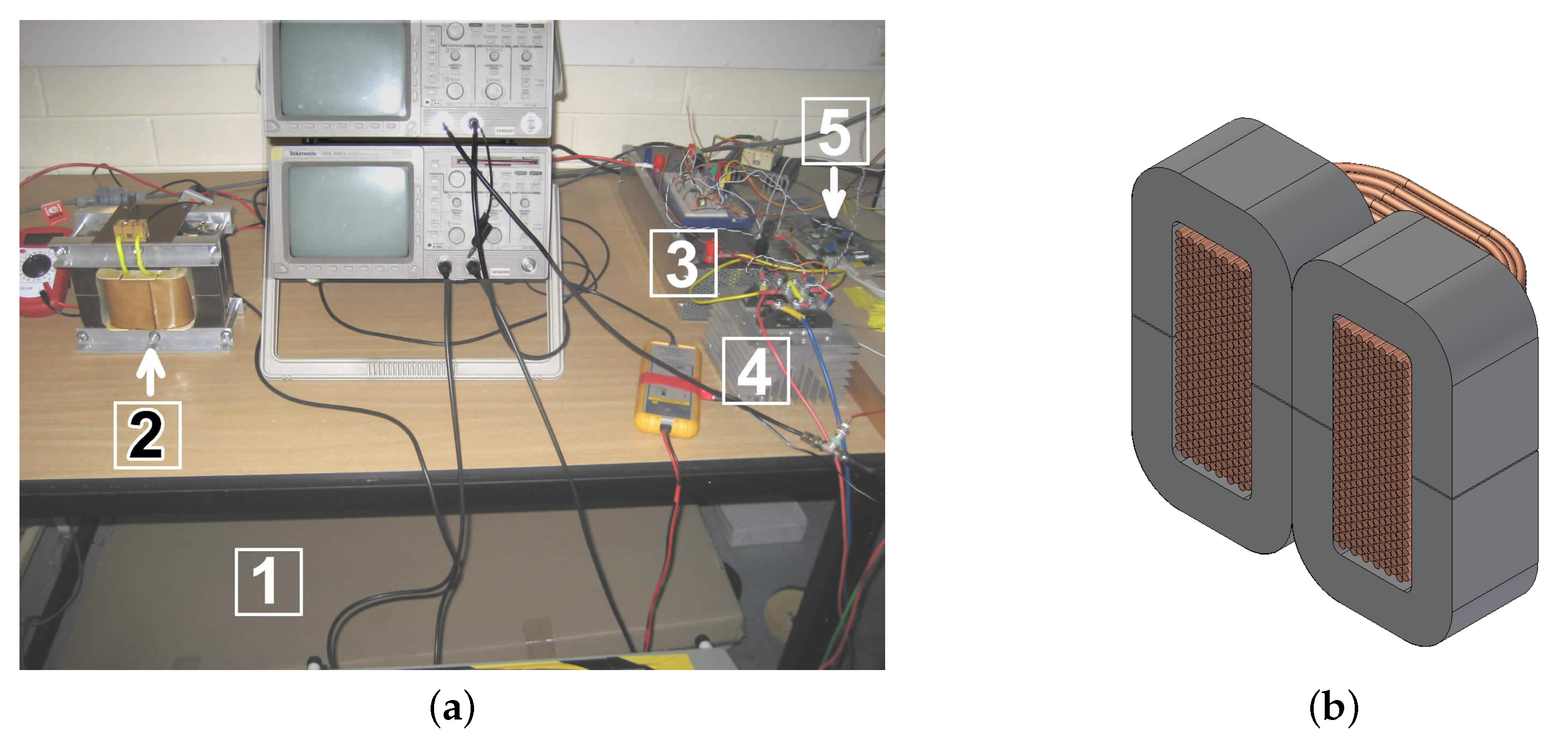
Figure 9a shows the GCI set-up in a laboratory. Two PV modules (BP380) were used in series as PV array simulator. They are fully covered and are fed by an external constant current-source with its magnitude set to produce the required irradiance value based on the dark I-V measurements [37]. Figure 9b shows the CAD drawing of the designed inductor before construction. Four iron C cores were used with 2 mm round wire to have less copper losses.
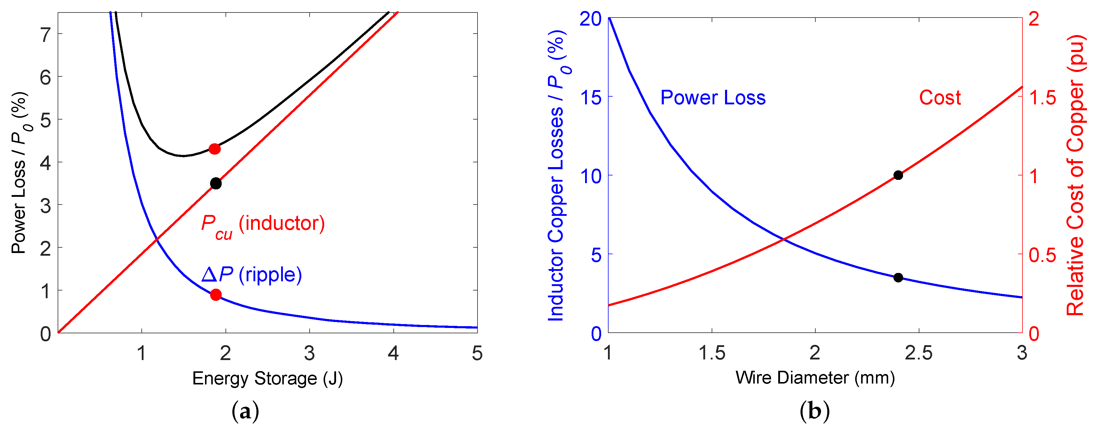
Figure 10a shows the mentioned total power loss (inductor copper loss curve and PV array power reduction) trade-off for a 160 W inverter that uses an optimized DC link inductor (192 mH). It is possible to have lower copper losses by increasing the size (and cost) of the inductor. The subfigure shows a trade-off between the two types of losses with the minimized power reduction of about 4.4%. Please note that the DC link energy storage losses would be much smaller, resulting in lower power reduction for a VSI. A trade-off concerning the decrease in copper losses, and at the same time the increase in the relative volume (hence cost) and packing factor of copper with an increase in the wire diameter, is shown in Figure 10b.
Two custom built inductors [38] are examined here for the 160 W CSI inverter, as listed in Table 3, which were designed to limit copper losses to 5 W at the rated PV array current () that corresponds to peak power (). The peak-to-peak current ripple (/) is around 13% for the 192 mH inductor. The stored energy is calculated from Equation (6), which allows other parameters, such as the inductance and the number of turns, etc., to be determined.
5. Experimental Results
5.1. Ripple Results
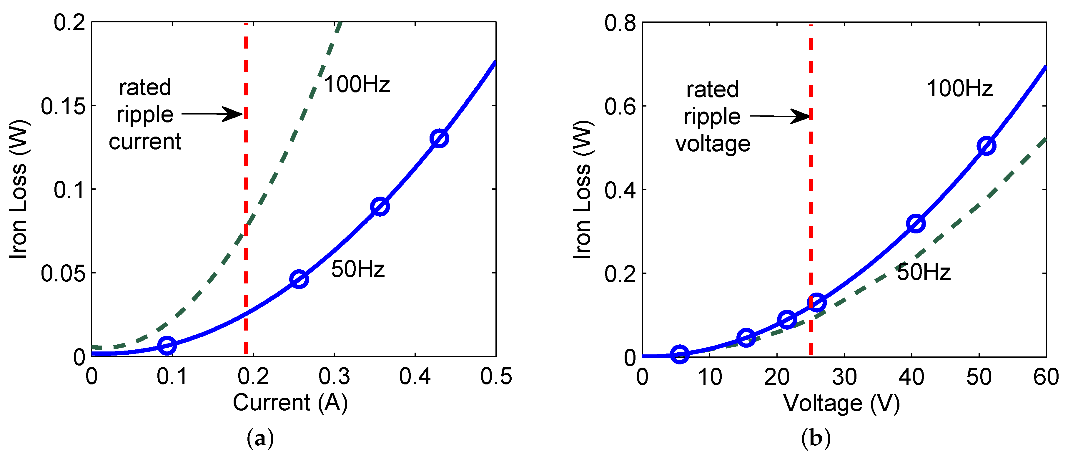
According to Table 2, the / value of the available voltage-source inverters is lower compared to the current-source inverters, which causes a significantly higher PV array current ripple and, therefore, mean PV array power reduction for the CSI. However, it is possible to decrease the aforementioned power reduction with the use of a physically bigger inductor, although this will cause increased iron losses in the inductor (see Figure 11a).
The iron losses shown consist of hysteresis and eddy-current losses, which are known to exist in a DC link inductor. Figure 11 presents the iron losses of the large inductor, which have been measured for different voltage and current values at 50 Hz. It was assumed that half of the iron loss is due to eddy-currents, and the other half is due to hysteresis. In such a case, the regular calculation of the losses with the 100 Hz variation was determined to be at approximately 0.08 W from the rated voltage ripple, as well as inductor current (see Table 4) at the MPP.
Figure 12 represents the simulated and experimentally tested input and output currents of the inverter, which are equal to the MPP of the PV array. The value of the current ripple is approximately 13.4%, and it matches well with the calculations, as seen in Table 3. Significant high-order harmonics require attention and optimization in the future, as evidence of resonances caused by the low-pass output filter in the inverter output current.
The main objective of an energy storage inductor is to maintain current in the DC link between the PV panels and the inverter free from fluctuations (minimize ripple). It is not possible to have a fluctuation-free current. Figure 12 and Figure 13a show the DC link current after the PV modules. For a single-phase system, the ripples at twice the line frequency are much larger compared to 3 systems and these significantly reduce the efficiency if there is insufficient energy storage device at the DC link. With a finite but large value of energy storage (e.g., 24 mJ/W), the PV panel voltage and current fluctuations are small; if the amount of energy storage is reduced, the fluctuations grow in amplitude. An additional circuit, such as a smoothing active parallel filter or extra circuitry at the DC link, can reduce fluctuations. However, these techniques would still require high amounts of energy storage to minimize the ripple, such that the current is free from fluctuations. Therefore, the design of the DC link inductor brings about trade-offs regarding the energy storage (hence size and volume) required, the copper losses associated with resistance, the reduction in PV output power, and the cost.
5.2. Modulation Index Results
An MPP tracking algorithm leads the CSI to operate at the peak operating point. However, the power reduction caused by fluctuations cannot be compensated by MPPT. These algorithms only change the average current or voltage to keep the power at MPP.
Given the effect of temperature on the cell output voltage, Figure 14a shows the simulated P-V characteristics for the PV array at under nominal conditions (25 C and 1000 W/m), as well as for a range of cell temperatures (75 C to −25 C). Under cold conditions, the PV array generates more output power; however, it also needs a higher (and, subsequently, a higher modulation index). Please note that the highest value of the is unity. The PV panel voltage will be lower than the maximum available if there is a limitation on the modulation index.
A critical operating parameter is the selection of the under nominal operating conditions (i.e., irradiance and cell temperatures); this is referred to as the nominal modulation index. The variation in PV array output power as a function of temperature for various points of the nominal is seen in Figure 14b. For low nominal modulation indices, there are a lot of margins to obtain a higher modulation index, which results in the maximum output power over the widest range of temperatures. However, if the nominal is unity, it is not possible to increase PV array’s output voltage beyond the value under nominal conditions; this represents a situation where under the cold conditions, the inverter would suffer from significant power reductions.
Note that, generally, an inverter’s efficiency increases with the , and, thus, there is a compromise between the inverter efficiency and the MPPT capability under this extreme cold condition. A value of nominal modulation ratio of 0.85 was selected for this analysis according to the results in Figure 14b. This results in a voltage ratio of 0.425, using Equation (9):
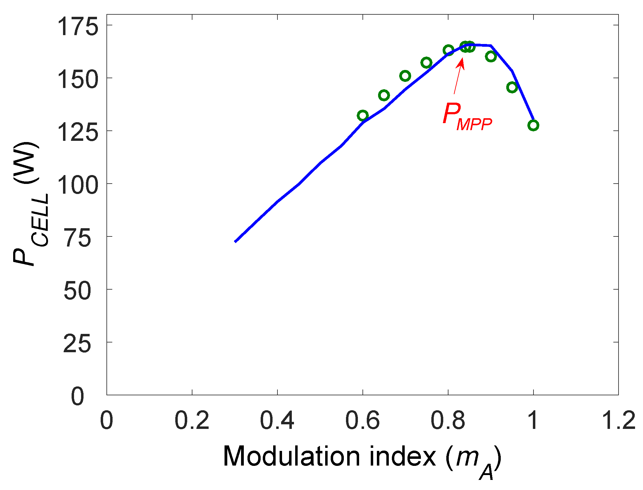
where represents the average PV array output voltage, represents the waveshaper input voltage, and represents the maximum value of the grid voltage. Figure 15 demonstrates the tested PV array power versus the modulation index for a 160 W current-source GCI. The PV array output power varies as a function of the modulation index. The selected nominal can be seen at the maximum power point.
The simulation and experimental results for the 160 W GCI which demonstrate PV array ripple and the DC link inductor losses are provided in Table 4.
The maximum power point values show a good agreement between the calculations and tests. Analysis of the the PV cell current ripple (), measured to be 13.4%, is similar to the simulated value of 13%. However, the calculated voltage ripple is significantly higher than that the measurement experimentally. This is explained below, where a power supply operating under constant current mode was used to drive the PV panel to simulate exposing it to sunlight (dark I-V test) [37]. The power supply used has a significant output capacitance which reduces its output impedance at 100 Hz. When the constant-current power supply was directly connected to the PV array, the measured voltage ripple was only about 30% of the simulated value. A 12 resistor was then connected in between the power supply and the PV array to increase its high-frequency output impedance. This increased the tested PV array voltage ripple to 60% of the simulated value. It would have been ideal to use a higher value series-connected resistor, however, the output voltage limitations of the power supply would not allow this. This effect also caused the PV array output power reduction to have a substantial error, as it was assumed that the power reduction was equal to half of the peak-to-peak ripple in the instantaneous PV array power.
A power analyzer (Voltech PM3000A, Voltech, Oxfordshire, U.K.) was used to obtain the loss breakdown of the inductor. The 100 Hz iron and copper losses were acquired with the harmonic analysis of the current and voltage waveforms. The tested DC copper and 100 Hz losses were subtracted from the total inductor loss to determine the PWM losses.
6. Conclusions
The main objective for the research presented in this paper has been to investigate the relationship between the PV array output fluctuation and the DC link energy storage for a single-phase GCI topology. The study was extended for a current-source GCI, as CSIs have substantially higher ripple at their DC link due to the reduced energy storage capacity of the DC link inductor. A summary of this work’s key findings, from the analysis, are listed below:
- The shapes of the normalized current-voltage (I-V) and power-voltage (P-V) curves, hence the power reduction, was not significantly affected by changes in cell temperature or irradiation;
- a more accurate estimation of PV output power loss was achieved using the “balanced” definition of current (or voltage) ripple. This is related to the equal power decrease at the extreme points in comparison to the case that the ripple was centered on the optimum point;
- utilizing this balanced method, the ripple magnitude versus average power reduction is close for both current and voltage ripple;
- the current and voltage ripple are directly related to the ratio of output power to energy stored in the DC link energy storage component;
- a trade-off exist between the average PV output power reduction and the DC link inductor size;
- two optimized DC link inductors were constructed to reduce the power loss due to fluctuating output power (at double the line frequency). However, only the 192 mH inductor was analyzed for (and tested with) the single-phase CSI. The conclusions from the experimental testing of this inductor include:
- -
- The total inductor loss is largely made up of copper losses due to the resistance of the DC link inductor and the high DC current;
- -
- other losses, such as those caused by hysteresis, eddy currents, and PWM switching scheme, caused small amount of the total losses; and
- -
- the test results closely agree with the PV output current ripple and DC link inductor loss calculations;
- the inverter efficiency increases with modulation index and, subsequently, a trade-off exists between the ability of the MPPT and the inverter efficiency, for cold conditions; and
- the normalized power reduction can be calculated, as this is related to the cell temperature, and a nominal modulation index can be selected.
This work provides a method to determine the minimal energy storage requirements, whilst keeping the average PV output power reduction within acceptable levels.
Author Contributions
Conceptualization, G.E., D.M.W., W.L.S. and N.E.; methodology, G.E. and W.L.S.; software, G.E., D.M.W. and W.L.S.; validation, G.E. and D.M.W.; formal analysis, G.E.; investigation, G.E., D.M.W. and W.L.S.; resources, N.E.; data curation, W.L.S, G.E. and D.M.W.; writing–original draft preparation, G.E.; writing–review and editing, D.M.W., G.E. and W.L.S.; visualization, G.E.; supervision, W.L.S. and N.E.; project administration, N.E. and W.L.S.
Funding
This research received no external funding.
Conflicts of Interest
The authors declare no conflict of interest.
References
- Rashid, M.H. Pulse-width-modulated inverters. In Power Electronics: Circuits, Devices, and Applications; Prentice-Hall: Upper Saddle River, NJ, USA, 1993; pp. 356–412. ISBN 0-13-334483-5. [Google Scholar]
- Kjaer, S.B. Design and Control of an Inverter for Photovoltaic Applications. Ph.D. Thesis, Aalborg University, Aalborg East, Denmark, 2004. [Google Scholar]
- Casadei, D.; Grandi, G.; Rossi, C. Single-phase single-stage photovoltaic generation system based on a ripple correlation control maximum power point tracking. IEEE Trans. Energy Conv. 2006, 21, 562–568. [Google Scholar] [CrossRef]
- Ninad, N.; Lopez, L.T. Operation of single-phase grid-connected inverters with large DC bus voltage ripple. In Proceedings of the 2007 IEEE Electrical Power Conference, Montreal, QC, Canada, 25–26 October 2007; pp. 172–176. [Google Scholar]
- Schonberger, J. A single phase multi-string PV inverter with minimal bus capacitance. In Proceedings of the 2007 IEEE Power Electronics and Applications Conference, Barcelona, Spain, 8–10 September 2009; pp. 1–10. [Google Scholar]
- Krein, P.T.; Balog, R.S.; Mirjafari, M. Minimum energy and capacitance requirements for single-phase inverters and rectifiers using a ripple port. IEEE Trans. Power Electron. 2012, 27, 4690–4698. [Google Scholar] [CrossRef]
- Zengin, S.; Deveci, F.; Boztepe, M. Decoupling capacitor selection in DCM flyback PV microinverters considering harmonic distortion. IEEE Trans. Power Electron. 2013, 28, 816–825. [Google Scholar] [CrossRef]
- Hu, H.; Harb, S.; Kutkut, N.; Sen, J.Z. A review of power decoupling techniques for microinverters with three different decoupling capacitor locations in PV systems. IEEE Trans. Power Electron. 2013, 28, 2711–2726. [Google Scholar] [CrossRef]
- Benavides, N.D.; Chapman, P.L. Modeling the effect of voltage ripple on the power output of photovoltaic modules. IEEE Trans. Ind. Electron. 2008, 55, 2638–2643. [Google Scholar] [CrossRef]
- Sullivan, C.R.; Awerbuch, J.J.; Latham, A.M. Decrease in photovoltaic power output from ripple: Simple general calculation and the effect of partial shading. IEEE Trans. Power Electron. 2013, 28, 740–747. [Google Scholar] [CrossRef]
- Bush, C.R.; Wang, B. A single-phase current source solar inverter with reduced-size DC link. In Proceedings of the 2009 IEEE Energy Conversion Congress and Exposition, San Jose, CA, USA, 20–24 September 2009; pp. 54–59. [Google Scholar]
- Zhu, G.-R.; Wang, H.; Liang, B.; Tan, S.C.; Jiang, J. Enhanced single-phase full-bridge inverter with minimal low-frequency current ripple. IEEE Trans. Ind. Electron. 2016, 63, 937–943. [Google Scholar] [CrossRef]
- Vitorino, M.A.; Hartmann, L.V.; Fernandes, D.A.; Silva, E.L.; Correa, M.B.R. Single-phase current source converter with new modulation approach and power decoupling. In Proceedings of the 2014 Applied Power Electronics Conference and Exposition, Fort Worth, TX, USA, 16–20 March 2014; pp. 2200–2207. [Google Scholar]
- Kotsopoulos, A.; Duarte, J.L.; Hendrix, M.A.M. Predictive DC voltage control of single-phase PV inverters with small DC link capacitance. In Proceedings of the 2003 IEEE International Symposium on Industrial Electronics, Rio de Janeiro, Brazil, 9–11 June 2003; pp. 793–797. [Google Scholar]
- Khajehoddin, S.A.; Karimi-Ghartemani, M.; Jain, P.K.; Bakhshai, A. DC-bus design and control for a single-phase grid-connected renewable converter with a small energy storage component. IEEE Trans. Power Electron. 2013, 28, 3245–3254. [Google Scholar] [CrossRef]
- Harb, S.; Mirjafari, M.; Balog, R.S. Ripple-port module-integrated inverter for grid-connected PV applications. IEEE Trans. Ind. Appl. 2013, 49, 2692–2698. [Google Scholar] [CrossRef]
- Zare, M.H.; Mohamadian, M.; Beiranvand, R. A single-phase grid-connected photovoltaic inverter based on a three-switch three-port flyback with series power decoupling circuit. IEEE Trans. Ind. Electron. 2017, 64, 2062–2071. [Google Scholar] [CrossRef]
- Krein, P.T.; Balog, R.S. Cost-effective hundred-year life for single-phase inverters and rectifiers in solar and LED lighting applications based on minimum capacitance requirements and a ripple power port. In Proceedings of the 2009 IEEE Applied Power Electronics Conference and Exposition, Washington, DC, USA, 15–19 February 2009; pp. 620–625. [Google Scholar]
- Kyritsis, A.C.; Papanikolaou, N.P.; Tatakis, E.C. Enhanced current pulsation smoothing parallel active filter for single stage grid-connected AC-PV modules. In Proceedings of the 2008 IEEE Power Electronics and Motion Control Conference, Poznan, Poland, 1–3 September 2008; pp. 1287–1292. [Google Scholar]
- Roman, I.T.; Silva, L.S. A single-phase current-source inverter with active power filter for grid-tied PV systems. In Proceedings of the 2012 IEEE International Symposium on Power Electronics for Distributed Generation Systems, Aalborg, Denmark, 25–28 June 2012; pp. 349–356. [Google Scholar]
- Ohnuma, Y.; Orikawa, K.; Itoh, J.-I. A single-phase current source PV inverter with power decoupling capability using an active buffer. IEEE Trans. Ind. Electron. 2015, 51, 531–538. [Google Scholar]
- Xiao, F.; Dong, L.; Liao, X. A single-phase grid-connected PV inverter with improved grid-connected current. In Proceedings of the 2015 IEEE Control and Decision Conference, Qingdao, China, 23–25 May 2015; pp. 4083–4088. [Google Scholar]
- Zhou, Y.; Li, H. A Single-Phase PV Quasi-Z-Source Inverter with Reduced Capacitance Using Modified Modulation and Double-Frequency Ripple Suppression Control. IEEE Trans. Power Electron. 2016, 31, 2166–2173. [Google Scholar] [CrossRef]
- Han, H.; Liu, Y.; Sun, Y.; Su, M.; Xiong, W. Single-phase current source converter with power decoupling capability using a series-connected active buffer. IET Power Electron. 2015, 8, 700–707. [Google Scholar] [CrossRef]
- Takahashi, H.; Takaoka, N.; Gutierrez, R.R.R.; Itoh, J. Power decoupling method for isolated DC to single-phase AC converter using matrix converter. In Proceedings of the 2014 IEEE Annual Conference of the Industrial Electronics Society, Dallas, TX, USA, 29 October–1 November 2014; pp. 3337–3343. [Google Scholar]
- Hwang, D.; Lee, J.; Cho, Y. PCC voltage compensation of PV inverter with active power decoupling circuit. In Proceedings of the IEEE International Power Electronics Conference, Niigata, Japan, 20–24 May 2018; pp. 1403–1408. [Google Scholar]
- Zhang, J.; Ding, H.; Wang, B.; Guo, X.; Padmanaban, S. Active power decoupling for current source converters: An overview scenario. Electronics 2019, 8, 197. [Google Scholar] [CrossRef]
- Ertasgin, G.; Whaley, D.M.; Ertugrul, N.; Soong, W.L. Analysis and design of energy storage for current-source 1-ph grid-connected PV inverters. In Proceedings of the 2008 IEEE Applied Power Electronics Conference and Exposition, Austin, TX, USA, 24–28 February 2008; pp. 1229–1234. [Google Scholar]
- Ertasgin, G.; Whaley, D.M.; Ertugrul, N.; Soong, W.L. Energy storage element sizing for single-phase grid-connected photovoltaic converter. In Proceedings of the IEEE Power Electronics and Motion Control Conference and Exposition, Rio de Janeiro, Brazil, 21–24 September 2014; pp. 1005–1010. [Google Scholar]
- Sreeraj, E.S.; Chatterjee, K.; Bandyopadhyay, S. One-cycle-controlled single-stage single-phase voltage-sensorless grid-connected PV system. IEEE Trans. Ind. Electron. 2013, 60, 1216–1224. [Google Scholar]
- Chen, Y.; Smedley, K.M. A cost-effective single-stage inverter with maximum power point tracking. IEEE Trans. Power Electron. 2004, 19, 1289–1294. [Google Scholar] [CrossRef]
- Neba, Y.; Furuyama, E. Calculation of maximum power in a utility-interactive photovoltaic-generating system by using PWM current-source inverter. Electron. Eng. Jpn. 1998, 125, 55–64. [Google Scholar] [CrossRef]
- Nonaka, S.; Kesamaru, K.; Yamasaki, K.; Nishi, M. Interconnection system with single-phase IGBT PWM CSI between photovoltaic arrays and the utility line. In Proceedings of the IEEE Industry Application Society, Seattle, DC, USA, 7–12 October 1990; pp. 1302–1307. [Google Scholar]
- BHC. Als 20/21 Series Screw Terminals—Plain and Stud Mountings. Available online: http://www.cd-aero.com/AerovoxHome.aspx (accessed on 4 March 2014).
- Ertasgin, G.; Whaley, D.M.; Ertugrul, N.; Soong, W.L. Implementation and performance evaluation of a low-cost current-source grid-connected inverter for PV applications. In Proceedings of the IEEE Sustainable Energy Technologies Conference, Singapore, 24–27 November 2008; pp. 939–944. [Google Scholar]
- Ertasgin, G.; Soong, W.L.; Ertugrul, N. Performance analysis of a low-cost current-source 1-ph grid-connected PV inverter. Turk. J. Elect. Eng. Comput. Sci. 2015, 23, 1985–1991. [Google Scholar] [CrossRef]
- King, D.L.; Hansen, B.R.; Kratochvil, J.A.; Quintana, M.A. Dark current-voltage measurements on photovoltaic modules as a diagnostic or manufacturing tool. In Proceedings of the IEEE Photovoltaic Specialists Conference, Anaheim, CA, USA, 29 September–3 October 1997; pp. 1125–1128. [Google Scholar]
- Erickson, W.R. Inductor design. In Fundamentals of Power Electronics, 2nd ed.; Kluwer Academic Publishers: New York, NY, USA, 2001; pp. 539–554. [Google Scholar]
Figure 1.
Conventional single-phase photovoltaic (PV) inverter topologies for (a) voltage-source; (b) current-source; and (c) two-stage voltage-source.
Figure 1.
Conventional single-phase photovoltaic (PV) inverter topologies for (a) voltage-source; (b) current-source; and (c) two-stage voltage-source.

Figure 2.
A common single-phase grid-connected current-source inverter (CSI) block diagram showing the PV array, inductor for energy storage, inverter and grid, and waveforms for power, voltage, and current.
Figure 2.
A common single-phase grid-connected current-source inverter (CSI) block diagram showing the PV array, inductor for energy storage, inverter and grid, and waveforms for power, voltage, and current.

Figure 3.
The output current fluctuations of a PV array which yield a decrease in the average power of PV array, for a CSI.
Figure 3.
The output current fluctuations of a PV array which yield a decrease in the average power of PV array, for a CSI.

Figure 4.
Voltage variations, reference to (a) irradiance; and (b) temperature at MPP.

Figure 5.
Illustration of (a) centered and (b) balanced assumptions for .

Figure 6.
Average power loss vs. voltage ripple (dashed lines) and current ripple (solid lines) using both assumptions. Circles represent the centered voltage ripple from Kjaer [2] for comparison purposes.
Figure 6.
Average power loss vs. voltage ripple (dashed lines) and current ripple (solid lines) using both assumptions. Circles represent the centered voltage ripple from Kjaer [2] for comparison purposes.

Figure 7.
The calculation procedure block diagram of the PV array power reduction. CSI = current-source inverter; VSI = voltage-source inverter.
Figure 7.
The calculation procedure block diagram of the PV array power reduction. CSI = current-source inverter; VSI = voltage-source inverter.

Figure 8.
Current-source GCI topology showing the PV inverter’s constant-current inputs, and the current waveforms for each stage.
Figure 8.
Current-source GCI topology showing the PV inverter’s constant-current inputs, and the current waveforms for each stage.

Figure 9.
(a) Current-source GCI set-up showing isolated PV modules (1), the 192 mH inductor (2), current waveshaper (3), SCR -based inverter (4), and microcontroller (5); (b) sectioned CAD drawing of the designed inductor, which illustrates windings and C cores.
Figure 9.
(a) Current-source GCI set-up showing isolated PV modules (1), the 192 mH inductor (2), current waveshaper (3), SCR -based inverter (4), and microcontroller (5); (b) sectioned CAD drawing of the designed inductor, which illustrates windings and C cores.

Figure 10.
Trade-off graphs of the inductor design, in which (a) total power loss vs. energy storage, and (b) the copper power loss and relative cost vs. wire diameter are presented. The values of the 192 mH inductor are indicated by circles.
Figure 10.
Trade-off graphs of the inductor design, in which (a) total power loss vs. energy storage, and (b) the copper power loss and relative cost vs. wire diameter are presented. The values of the 192 mH inductor are indicated by circles.

Figure 11.
Iron loss vs. (a) coil current and (b) voltage, for the 192 mH inductor. Circles represent measurements at 50Hz, and the dashed line represents estimated losses at 100 Hz double line frequency.
Figure 11.
Iron loss vs. (a) coil current and (b) voltage, for the 192 mH inductor. Circles represent measurements at 50Hz, and the dashed line represents estimated losses at 100 Hz double line frequency.

Figure 12.
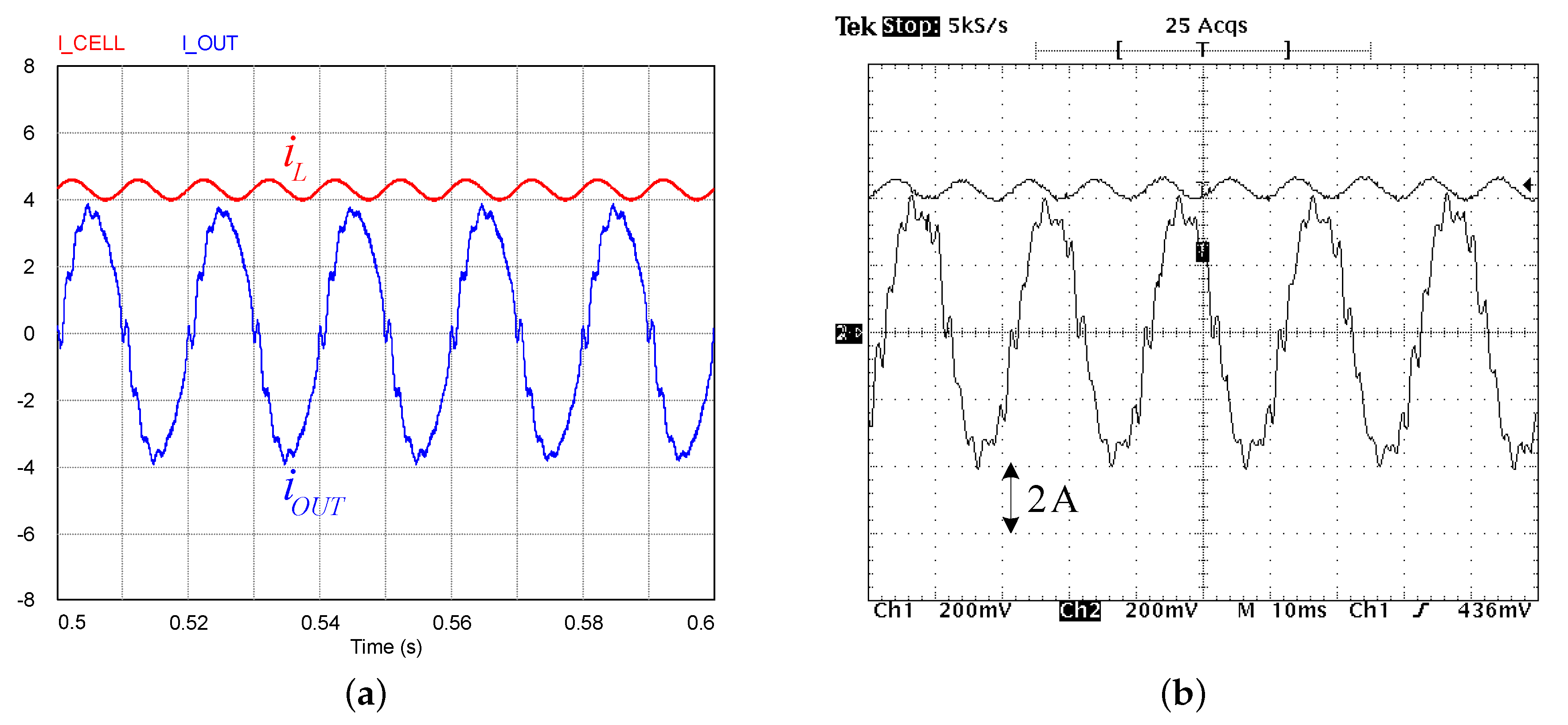
The (a) simulated and (b) experimentally measured PV array output and the inductor ripple () and CSI output () currents.
Figure 12.
The (a) simulated and (b) experimentally measured PV array output and the inductor ripple () and CSI output () currents.

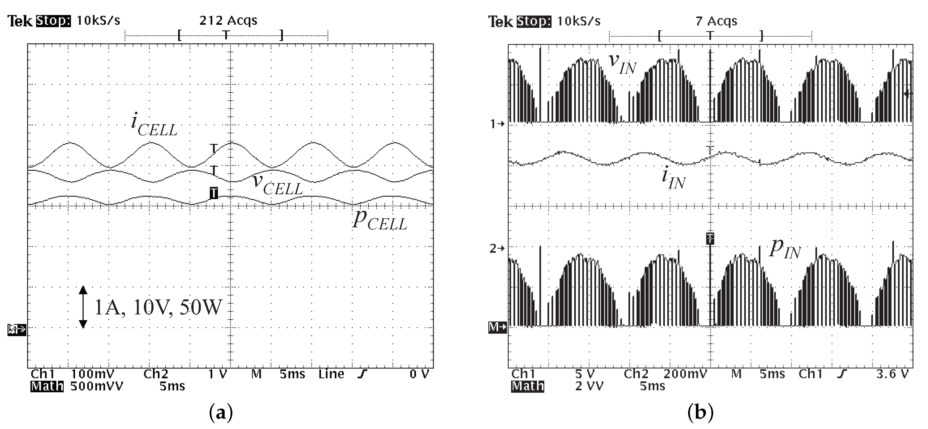
Figure 13.
The measured (a) PV array current, voltage, and power waveforms, and (b) CSI input voltage, current, and power waveforms.
Figure 13.
The measured (a) PV array current, voltage, and power waveforms, and (b) CSI input voltage, current, and power waveforms.

Figure 14.
(a) PV array output power variation as a function of PV array output voltage at MPP and (b) normalized power reduction vs. temperature at MPP.
Figure 14.
(a) PV array output power variation as a function of PV array output voltage at MPP and (b) normalized power reduction vs. temperature at MPP.

Figure 15.
Experimental and simulation results of the PV cell output power in the form of a function of modulation index. Simulation is shown with a solid line, and experimental results are shown with points.
Figure 15.
Experimental and simulation results of the PV cell output power in the form of a function of modulation index. Simulation is shown with a solid line, and experimental results are shown with points.


Table 1.
Impact of various normalizations on the I-V and P-V loci of the BP380 module under the conditions of changing irradiance and temperature. MPP = maximum power point.
Table 1.
Impact of various normalizations on the I-V and P-V loci of the BP380 module under the conditions of changing irradiance and temperature. MPP = maximum power point.
| Model | Irradiance Changes | Temperature Changes |
|---|---|---|
| Actual |  |  |
| Norm. at MPP under nom. |  |  |
| Norm. all at MPPs |  |  |
Table 2.
Available voltage-source and current-source PV grid-connected inverter (GCI) design examples, with respect to the balanced definition. PV array power reduction, power loss due to DC link component, and total loss are provided [28]. ESR = equivalent series resistance.
Table 2.
Available voltage-source and current-source PV grid-connected inverter (GCI) design examples, with respect to the balanced definition. PV array power reduction, power loss due to DC link component, and total loss are provided [28]. ESR = equivalent series resistance.
| VSI | CSI | |||
|---|---|---|---|---|
| Reference | [30] | [31] | [32] | [33] |
| Grid frequency | 50 Hz | 60 Hz | 60 Hz | 60 Hz |
| Rated max. input power | 205 W | 600 W | 225 W | 408 W |
| Capacitance | 1.1 mF | 3 mF | - | - |
| Inductance | - | - | 200 mH | 400 mH |
| Input current for () | 1.74 A | 4.4 A | 5.7 A | 6.15 A |
| Input voltage for () | 118 V | 136.3 V | 45 V | 66.3 V |
| Energy storage per W. | 37.1 mJ | 46.4 mJ | 14.4 mJ | 18.5 mJ |
| Ripple | 5 V | 3.82 V | 0.6 A | 0.44 A |
| Ripple (%) | 4.3 | 2.8 | 10.6 | 7.1 |
| PV array power reduction (%) | 0.17 | 0.05 | 1 | 0.46 |
| Capacitor ESR | 12 m | 14 m | - | - |
| Inductor resistance | - | - | 1.3 | - |
| loss (%) | 0.018 | 0.05 | 16 | - |
| Total Power loss (%) | 0.19 | 0.1 | 17 | - |
Table 3.
Inductor specifications for the PV CSI [28].
Table 3.
Inductor specifications for the PV CSI [28].
| Parameter | Inductor 1 | Inductor 2 |
|---|---|---|
| Rated maximum input power () | 160 W | 160 W |
| Input current for () | 4.5 A | 4.5 A |
| Input voltage () | 35 V | 35 V |
| Inductance (L) | 112 mH | 192 mH |
| Stored energy | 1.15 J | 1.96 J |
| Diameter of the copper wire | 2.4 mm | 2.4 mm |
| Number of turns (N) | 249 | 200 |
| Resistance at 40 C () | 0.25 ohm | 0.324 ohm |
| Power losses in the inductor () | 5.0 W | 6.7 W |
| Current ripple (peak-to-peak) | 21.3 % | 12.8 % |
| Peak flux density (B) | 1.5 T | 1 T |
| Copper winding packing factor | 0.46 | 0.37 |
| Volume | 0.00052 m | 0.0021 m |
| Mass | 5.5 kg | 15.5 kg |
Table 4.
DC link inductor measurement results for 160 W GCI [28].
Table 4.
DC link inductor measurement results for 160 W GCI [28].
| 192 mH Inductor | ||
|---|---|---|
| Calculated | Tests | |
| Maximum Power Point | ||
| 38.3 V | 36.97 V | |
| 4.33 A | 4.39 A | |
| 166.6 W | 162.9 W | |
| PV array ripple analysis | ||
| (p-p) | 12.7% | 7.6% |
| (p-p) | 13.0% | 13.4% |
| (p-p) | 2.65% | 6.10% |
| (ripple) | 1.33% | 3.10% |
| Total PV power reduction | 2.22 W | 5.00 W |
| Inductor losses | ||
| DC copper loss | 6.07 W | 5.86 W |
| 100 Hz copper + iron loss | 0.09 W | 0.15 W |
| PWM loss | - | 0.10 W |
| Total inductor loss | 6.16 W | 6.11 W |
| PV array power reduction | 8.38 W | 11.11 W |
| and inductor losses | ||
© 2019 by the authors. Licensee MDPI, Basel, Switzerland. This article is an open access article distributed under the terms and conditions of the Creative Commons Attribution (CC BY) license (http://creativecommons.org/licenses/by/4.0/).
Share and Cite
MDPI and ACS Style
Ertasgin, G.; Whaley, D.M.; Ertugrul, N.; Soong, W.L. Analysis of DC Link Energy Storage for Single-Phase Grid-Connected PV Inverters. Electronics 2019, 8, 601. https://doi.org/10.3390/electronics8060601
AMA Style
Ertasgin G, Whaley DM, Ertugrul N, Soong WL. Analysis of DC Link Energy Storage for Single-Phase Grid-Connected PV Inverters. Electronics. 2019; 8(6):601. https://doi.org/10.3390/electronics8060601
Chicago/Turabian StyleErtasgin, Gurhan, David M. Whaley, Nesimi Ertugrul, and Wen L. Soong. 2019. "Analysis of DC Link Energy Storage for Single-Phase Grid-Connected PV Inverters" Electronics 8, no. 6: 601. https://doi.org/10.3390/electronics8060601
Note that from the first issue of 2016, this journal uses article numbers instead of page numbers. See further details here.