Shaping SiC MOSFET Voltage and Current Transitions by Intelligent Control for Reduced EMI Generation


School of Automation Science and Electrical Engineering, Beihang University, Beijing 100191, China
*
Author to whom correspondence should be addressed.
Electronics 2019, 8(5), 508; https://doi.org/10.3390/electronics8050508
Submission received: 11 April 2019
/
Revised: 27 April 2019
/
Accepted: 2 May 2019
/
Published: 8 May 2019
(This article belongs to the Special Issue Power Converters in Power Electronics)
Abstract
:In power converters, the fast switching of the power conversion components results in rapid changes in voltage and current, which results in oscillations and high-level electromagnetic interference (EMI), so the power components become a source of internal electromagnetic interference. Taking SiC Metal-Oxide-Semiconductor Field-Effect Transistor (MOSFET) as an example, an intelligent control method to suppressing interference sources is proposed in this paper. The combination of open-loop and closed-loop methods can simultaneously reduce the electromagnetic interference generated by voltage and current. Firstly, this paper analyzes how to select a reference signal. The relationship between the time domain and the frequency domain of the noise signal is analyzed. The convolution of the trapezoidal signal and the Gaussian signal is selected as the reference signal, which is named S-shaped signal in this paper. The S-shaped signal has continuous infinitely conductive characteristics, so its spectrum has a large attenuation in the high frequency region. Secondly, a new topology is proposed. Based on the closed-loop gate control, a current control signal is added, which can simultaneously shape the output voltage and control the output current slope. Both the simulation results and the experimental results show that the output voltage can follow the reference signal, S-shaped signal, and the slope and overshoot of output current can be changed. Compared with classical gate driver method, the spectrum of output voltage and output current obtained by the method proposed in this paper has a large attenuation, in other words, the electromagnetic interference is significantly reduced.
1. Induction
Power converters composed of SiC MOSFETs are widely used in home, aerospace, and other fields due to their high operating frequency, high voltage, and high power density. However, due to the high dv/dt and di/dt of SiC MOSFET for high-speed switching, electromagnetic interference (EMI) is generated so that the SiC MOSFET becomes an electromagnetic interference source [1]. High dv/dt may produce common mode interference signals in power electronic circuits, while higher di/dt can cause higher voltage and current overshoot and oscillation due to parasitic factors in the circuit. The EMI signal can easily affect external sensitive components by radiation or conduction. It is common to reduce conducted interference by adding filters in the conduction path and radiated interference by shielding sensitive components. However, these two methods will take up more PCB space and increase the cost greatly. It is a challenge for engineers to balance the suppression effect of electromagnetic interference and costs [2]. Therefore, it is an interseting research direction that is suppressing EMI by controlling the fast switching transient [3]. Changing gate driving current [4], and using a built-in snubber [5] all have limited effect for suppressing EMI. Active voltage control (AVC) method is applied to control the slope dv/dt of the output voltage, which is effective to control the switching transients of IGBT to reduce the EMI [6]. References [7,8,9] introduced how to predict the EMI for the defined edges of signal and what the influence of the defined reference signal is for the transients of IGBT, which provided the possibility to shape the Gaussian switching transients to suppress EMI. The active gate drive (AGD) method is an effective method for suppressing electromagnetic interference from the viewpoint of suppressing electromagnetic interference sources. The AGD method mainly includes three methods: controlling the gate current, controlling the gate voltage, and controlling the gate resistance. References [10,11] applied a method of controlling the gate current to control the switching transient. During the turn-off period of SiC MOSFET, a large current is injected into the gate to increase dv/dt to reduce the turn-off time and the turn-off loss is reduced thereby. When the output current drops, the rapidly decreasing gate current reduces the di/dt of the output current and the oscillation of the voltage generated by the inductance and parasitic capacitance is reduced. However, the dv/dt of the output voltage is not adjustable.
Reference [12] proposes a method of controlling the gate current by closed-loop and adding a delay compensation device to control the gate source turn-off voltage slope dv/dt and current slope di/dt, thereby achieving the trade-off between switching losses and electromagnetic interference. However, this method also has its limitations, because it can only control dv/dt and di/dt when MOSFET is closed. A new method of active gate drive method is proposed Reference [13], the principle of which is to increase the gate resistance value during the Miller plateau of the gate voltage during the turn-on and turn-off of the SiC MOSFET. This control method can control di/dt during turn-on and dv/dt during turn-off, respectively, and its switching loss is low. This control method can control di/dt during turn-on and dv/dt during turn-off, respectively, and its switching loss is low but this method cannot control dv/dt during turn-on and di/dt during turn-off. The precondition for this method to work properly is to select the correct switching time of gate resistance and the gate voltage cannot have large fluctuations, however, which is difficult to implement in engineering. In [14], the closed-loop control method is applied and di/dt and dv/dt are measured and then compared with reference signals to get the error. The error is input to the buffer pole through a differential op amp to dynamically adjust the gate voltage. The power semiconductor is turned on by the waveform following the reference signal. However, it is impossible to adjust dv/dt without di/dt restrictions because the same reference and the same gain are used [4]. All of the above methods of controlling a single dv/dt or di/dt have limited suppression of high frequency noise, and fail to achieve simultaneous control of voltage and current turn-on and turn-off. The results of reference [1] indicate that any switching waveform can be expressed in the form of convolution that it is get by an ideal square wave signal and a normalized instantaneous function derivative. From a frequency domain perspective, the switching waveform is the product of the square wave signal spectrum and the instantaneous function derivative spectrum. Reference [15] shows that if the transient function can be derived n times, the high-frequency spectral envelope of the switching waveform will be attenuated by a slope of −20(n + 1) dB/dec. The Gaussian signal has continuous infinitely conductive characteristics, so that the high frequency spectrum of the Gaussian waveform is attenuated faster than the high frequency spectrum of the single slope theoretically. Therefore, in [2], the convolution waveform of the square wave signal and the Gaussian signal as the reference signal is used, and the switching voltage following the reference voltage by the method of closed-loop active voltage control is realized.
This paper proposed an intelligent control method based on the characteristic that voltage and current are not synchronized during SiC MOSFET switching. The intelligent control method that include a closed-loop circuit to shape the output voltage and an open-loop circuit to control the slope of the output current control the switching voltage and current simultaneously.
The article is organized as follows: Theoretical analysis of voltage reference signals and current control signals is discussed in the Section 2. An intelligent control method combining closed-loop and open-loop control methods is proposed in the Section 3. Simulation and experimental verification were performed based on the proposed method in Section 4 and Section 5. The conclusion of the experiment is presented in Section 6.
2. Theoretical Analysis
2.1. Selection of Voltage Reference Signal
In order to make the output voltage have a smooth transient during turn-on and turn-off period, it is a feasible method to select an appropriate reference signal in closed-loop control circuit. Therefore, the paper discussed how to select the reference signals first. Reference [1] discussed the effects of time domain parameters on the frequency domain envelope of the signal. The relationship between the number of derivatives of the transient signal in the time domain and the envelope of the high frequency component of the signal in the frequency domain is discussed in [15] that plays an important role to guide this paper. According to [16], a brief review of how to select the reference signal is shown as follows.
It is assumed that the switching transient waveform is represented by sw(t), and its image is shown in Figure 1a. Its expression is assumed as follow Equation (1)
where s(t) is the switching transient function, A is the amplitude of the switching signal that is a constant, τ is the rise time and fall time, T is the switching period of the signal, t0 is the signal width of square wave.
t < 0: sw(t) = 0
0 < t < τ: sw(t) = s(t)
τ < t < t0: sw(t) = A
t0 < t < t0 + τ: sw(t) = A − s(t − t0)
t0 + τ < t < T: sw(t) = 0
0 < t < τ: sw(t) = s(t)
τ < t < t0: sw(t) = A
t0 < t < t0 + τ: sw(t) = A − s(t − t0)
t0 + τ < t < T: sw(t) = 0
Figure 1b explains how to get sw(t). The switching signal, sw(t), can be expressed as the convolution of the square wave signal sq(t) with 1/A*ds(t)/dt that is the normalized derivative of the transient function. The equation is
sw(t) = sq(t)*(1/A.ds(t)/dt) = sq(t)*g(t)
Perform the Fourier transform on Equation (2) and get the following Equation (3)
sw(f) = sq(f).g(f)
Obviously, it can be seen from Equation (3) that the switching signal sw(f) can be regarded as the product of the Fourier transform of a square wave signal and a shaped smoothing function.
According to [1], in the frequency domain, the slope of the envelope of sw(f) is closely related to the derivative times k of the function in the time domain. It is supposed that sw(k)(t) shows discontinuity and P Dirac pulses will appear in sw(k+1)(t) after the (k + 1) times derivative.
τi and Ai are the times and amplitudes of the Dirac pulse. The expression of Fourier transform on (4) is
where w0 = 2π/T, Fs(n) is the coefficient of the Fourier transform of sw(t). The expression of Fs(n) is as Equation (6)
From Equation (6), high-frequency harmonics coefficients is get as Equation (7) when .
It can be seen from (7) that for an arbitrary waveform, the high-frequency boundary amplitude is determined by the sum of its derivative times k, P Dirac pulses amplitude and its fundamental frequency f0 = w0/2π in the frequency domain. The attenuation envelope slope is −20(k + 1) in the high-frequency domain. In order to verify the higher frequency, the derivatives times of the function, the better the high-frequency EMI suppression effect [17], the following examples are used.
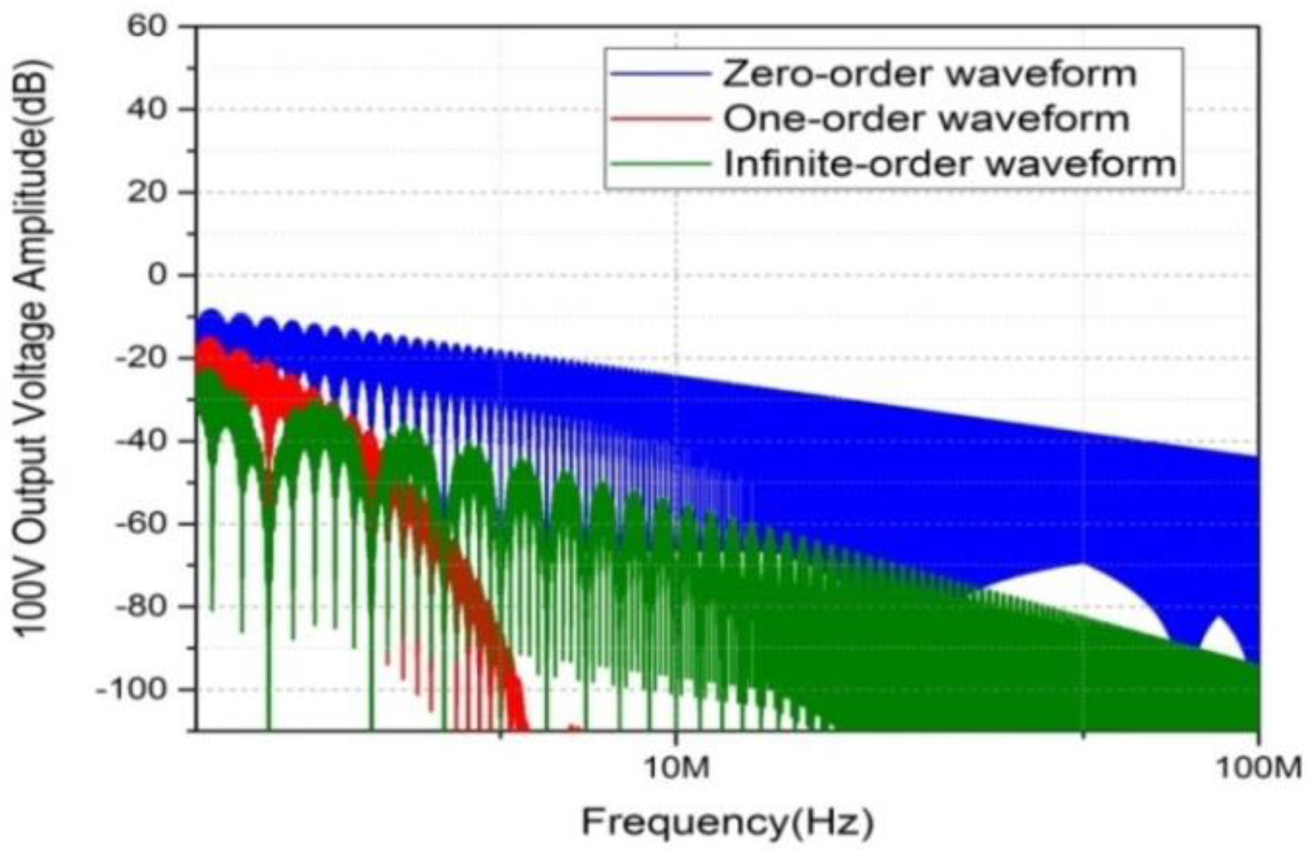
We define the zero-order signal to be the square signal and two-order signal to be the symmetrical trapezoidal signal. Infinite-order signal, , can be expressed as the convolution of a square wave signal and a Gaussian signal. Their expressions are
where g0(t) is a square signal, gS(t) = is a Gaussian signal. The mentioned zero-order signal and two-order signal that we selected both are symmetric signal. The duty cycle is D = 0.5, the switching frequency is 10 kHz, rise time is toff = 1 µs, fall time is tfall = 10 µs, .
sw1(t) = q0(t)*g0(t)
sw∞(t) = q0(t)*gs(t)
The spectrum of q0(t), and are shown in Figure 2. It is worth mentioning that only time t is|t| → ∞, the Gaussian function is gS(t) → 0. In other words, the value of Gaussian function is not strictly equal to 0 in a finite period so there is a theoretical limitation. However, when |t| ≥ 2σt, the Gaussian value is close to 0. Therefore, if is taken, the value of Gaussian function can be regarded as 0 at the two endpoints of the finite time.
From Figure 1, it can be seen that the high frequency component of one-order signal (trapezoidal signal) is lower than zero-order signal (square signal) and the high frequency component of infinite-order signal (Gaussian signal) is lower than one-order signal, which is consistent with the theory that the higher the derivative times is, the better the suppression effect on high frequency noise is.
2.2. Control Principle for Current
According to the literature [18], the derivative of the drain current to time, is expressed as Equation (10) when the MOSFET is turned on.
where Vgg is the gate voltage, Vth is the threshold voltage, Lg is the gate parasitic inductance, (Cgs gate source parasitic capacitance, Cgd gate drain parasitic capacitance), gm is transconductance, gate resistance at turn-on and Ls is the source parasitic inductance. The drain reverse recovery current is given by (11) [19].
where is the reverse recovery charge and S represents the fast factor. It can be seen from (10) (11) that the reverse recovery current and current overshoot can be controlled by changing the Vgg.
During turn-on period for MOSFET, the derivative of the drain current to time is given by (12)
where Vee is the gate voltage at turn-off for MOSFET. From (12), the slope of the drain voltage can be controlled by changing the gate voltage Vee during turn-off period.
3. Proposed Intelligent Control Method and Operation Principle
The total circuit diagram used in the proposed intelligent control method for voltage and current is shown in Figure 3. The circuit consists of an open-loop circuit, a closed-loop circuit and a conventional totem pole drive. The drain-source voltage Vds of the SiC MOSFET is shaped by the closed-loop circuit in the upper side. When Logic1 outputs 1, switches S1 and S2 are turned on at the same time, the closed-loop circuit starts to work and the drain voltage is fed back by the drain voltage feedback circuit to the positive terminal of the operational amplifier according to the ratio β. The feedback signal is compared with a reference signal generated by the reference signal generator 1, and the gate of the SiC MOSFET is controlled by a totem pole drive circuit. When Logic2 outputs 1, the switches S3 and S4 are turned on, and the current control signal Vi control the gate voltage by the operational amplifier 2. It is necessary to add a resistor Rg to the gate to connect the gate to prevent the SiC MOSFET from operating outside the safe zone. Another function for the Rg is to reduce the oscillation of voltage and current when turned on and off. The value of Rg can be selected according to the values recommended in the datasheet. In this paper, its value is 5 ohms.
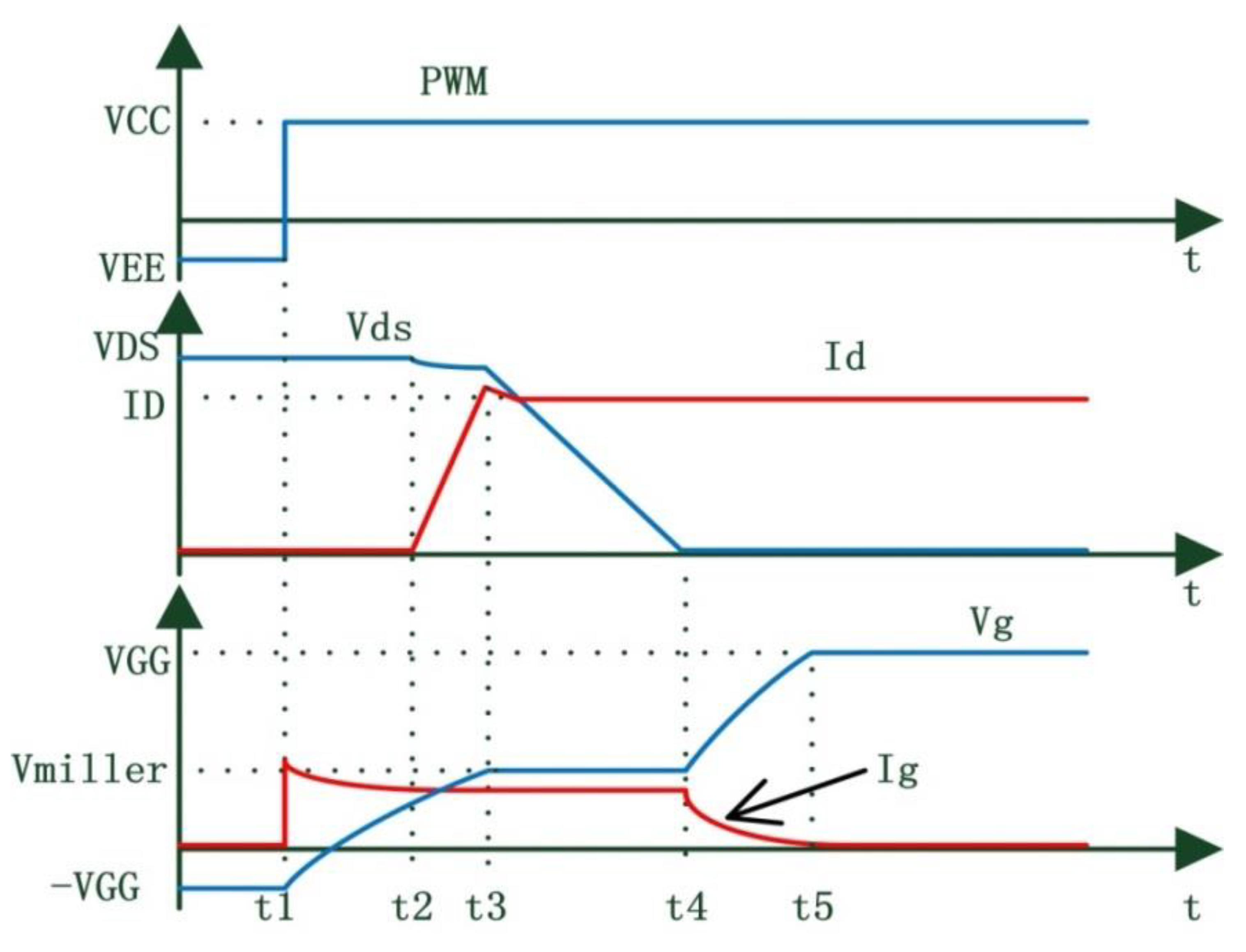
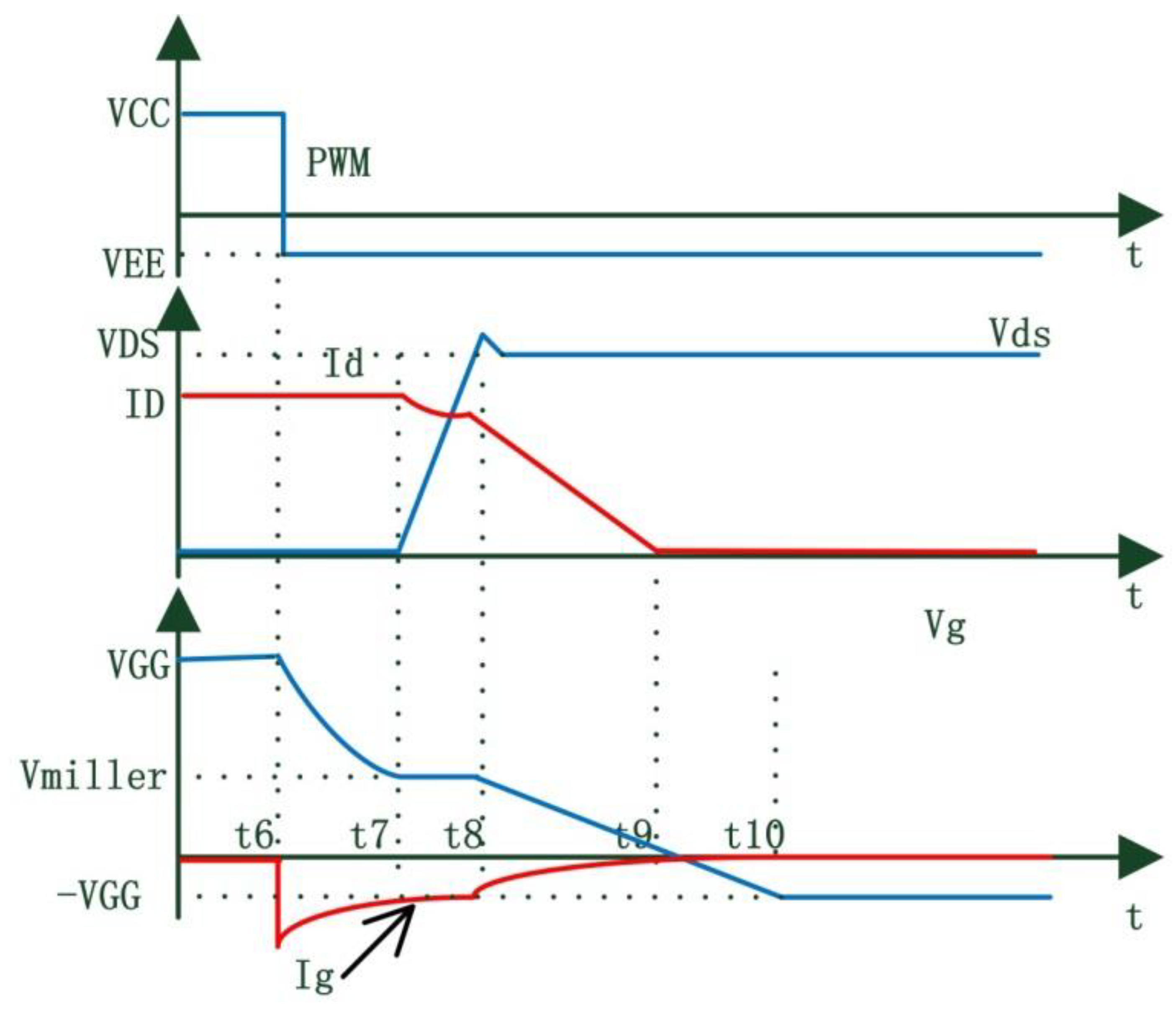
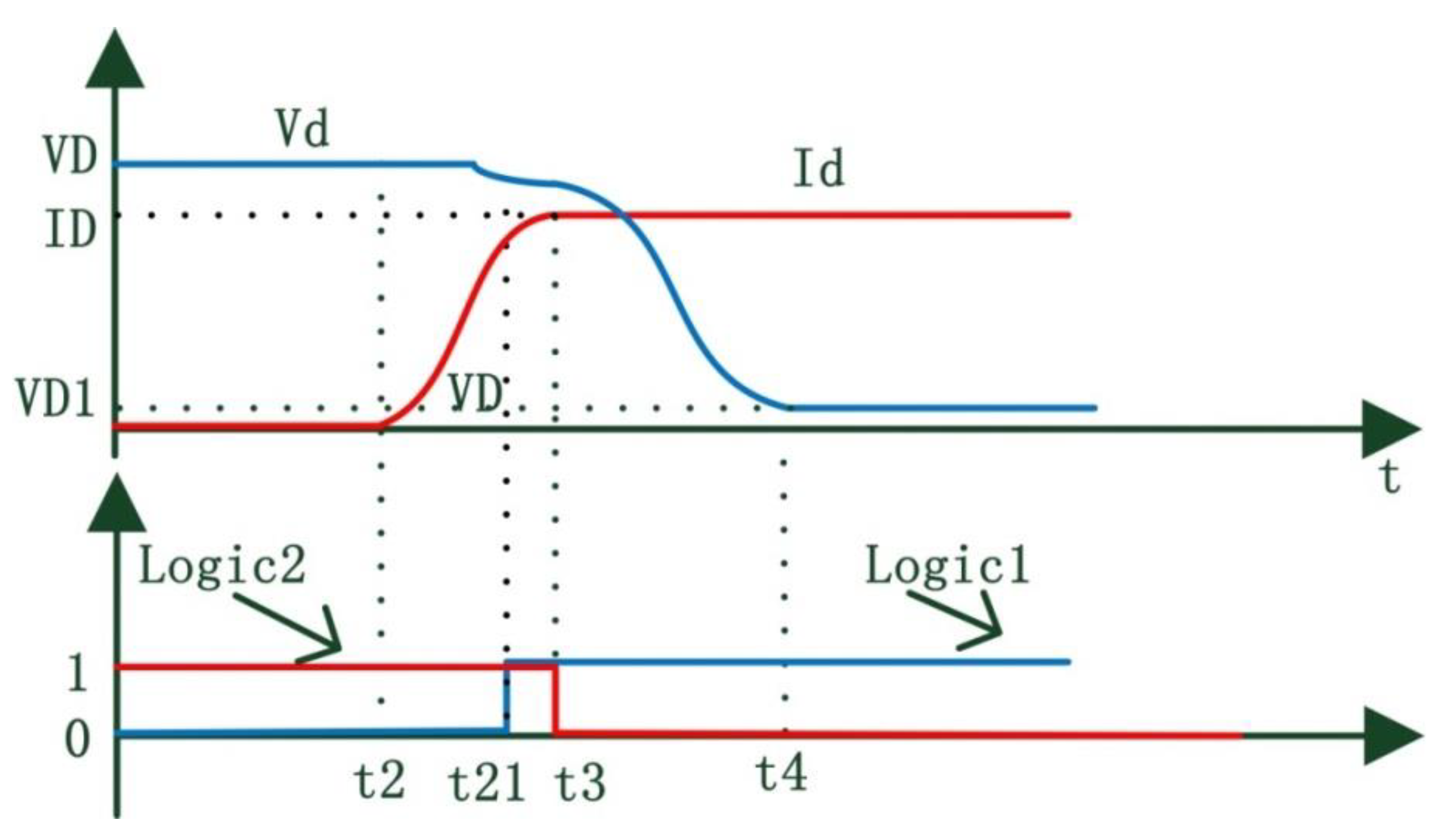
The control signal selected is the Gaussian signal in this paper, which is generated by arbitrary waveform generator, M3202A, according to Equation (11). The proposed intelligent control method for voltage and current is based on fact that the current and voltage are not synchronized during MOSFET switching period. Figure 4 and Figure 5 show the time domain signal of the SiC MOSFET during turn-on and turn-off period under hard switching conditions respectively. During the period from t2 to t3, the current Id rises firstly, and the voltage Vd has a small decrease (in order to simplify the analysis, Vd is regarded as unchanged in this paper). At the time t3, the current rises to the maximum, the voltage begins to drop rapidly, and it drops to the lowest moment. During the period from t7 to t8, the voltage Vd rises rapidly, and the current Id has a small drop (to simplify the analysis, the Id does not change during this time period). At t8, the voltage Vd (Drain voltage) gets the maximum value. The current Id drops rapidly after t8 and the current gets the minimum value t9. Therefore, the drain voltage and current of SiC MOSFET are not synchronized during switching period, which provides a possibility for intelligent control.
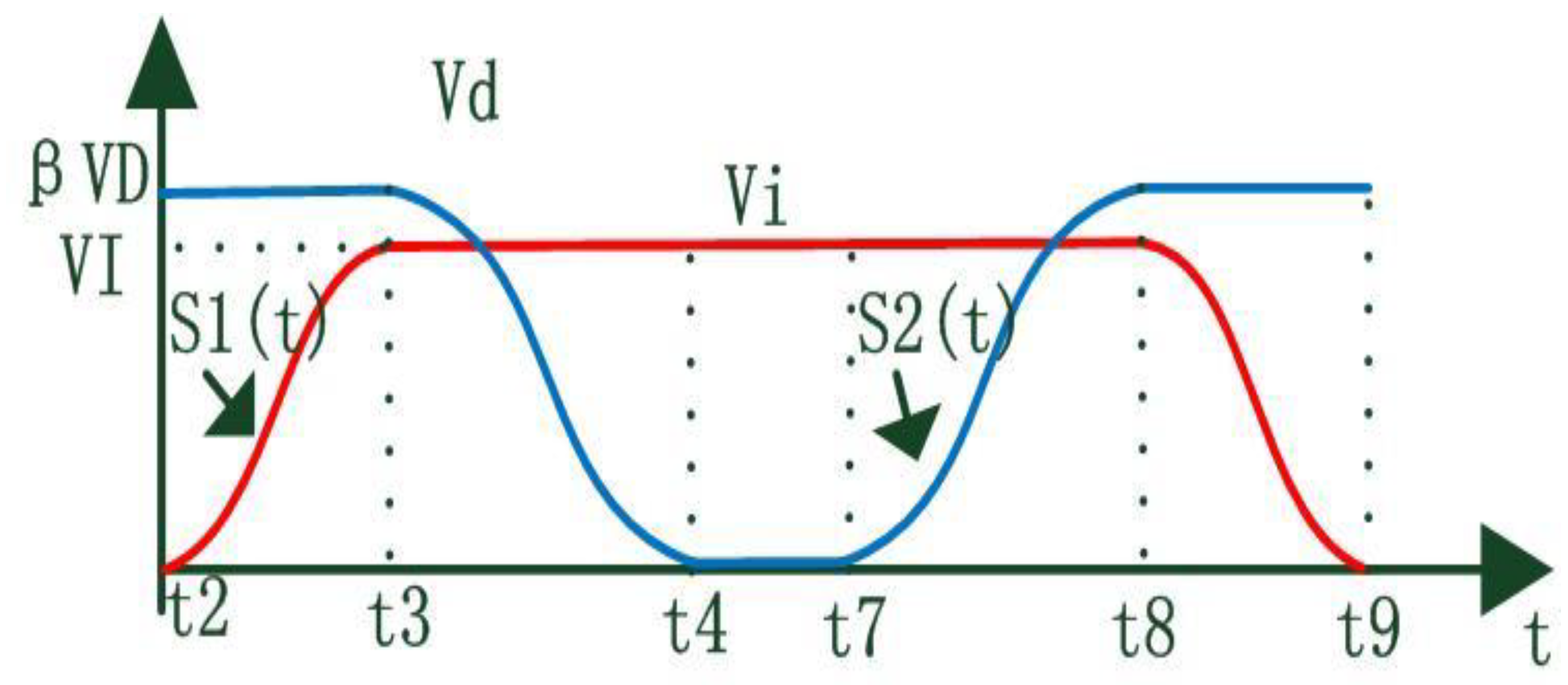
Time domain diagram of Gaussian control signals for voltage and current is shown in Figure 6. S1(t) and S2(t) are rising edges for drain voltage and current respectively and the falling edge signal is symmetric with the rising edge signal. They can be obtained by Equation (11).
Figure 7 and Figure 8 are the theoretical waveforms of the voltage and current of the proposed intelligent control for turn-on and turn-off, respectively. The switch S3 is turned on and the current control signal is connected to the circuit to control the output current during the 0–t3 period. At time t3, switch S3 is opened and the open-loop circuit stop working. It should be noted that S1 and S2 are closed at time t21 that is before time t3. The delay time for switches S1 and S2 is td1 = t3 − t21. The delay time is caused by MOSFET, operational amplifier, and coupling circuit, which must be taken into account to make the upper part of the circuit achieve the best turn-on transient behavior, when the open-loop stops working. In contrast to the turn-on transient, S1 and S2 are turned on during the t21–t8 period and the voltage closed-loop operates normally. At time t8, S1 and S2 are turned off. However, S3 is turned on at time t71 that is before time t8. This is because a delay time td2 = t8 − t71 is required to achieve current control after the switch S3 turned-on. The delay time that we concerned to cause by MOSFET, operational amplifier, and coupling circuit guarantees that MOSFET has an optimal turn-off behavior transient. The values of td1 and td2 can be dynamically adjusted to determine the optimum value, according to the switching voltage and current transients of the MOSFET.
4. Circuit Simulation and Discussion
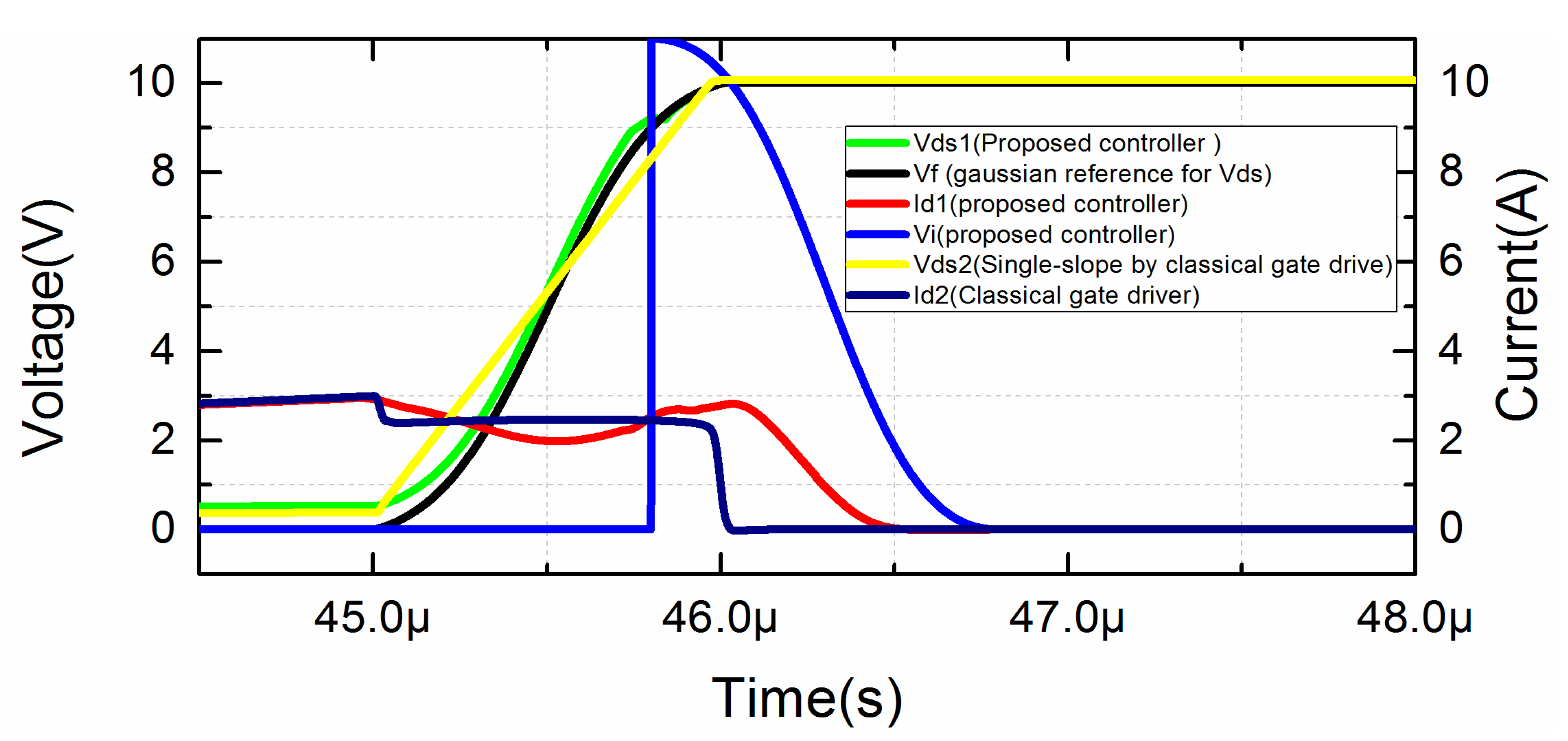
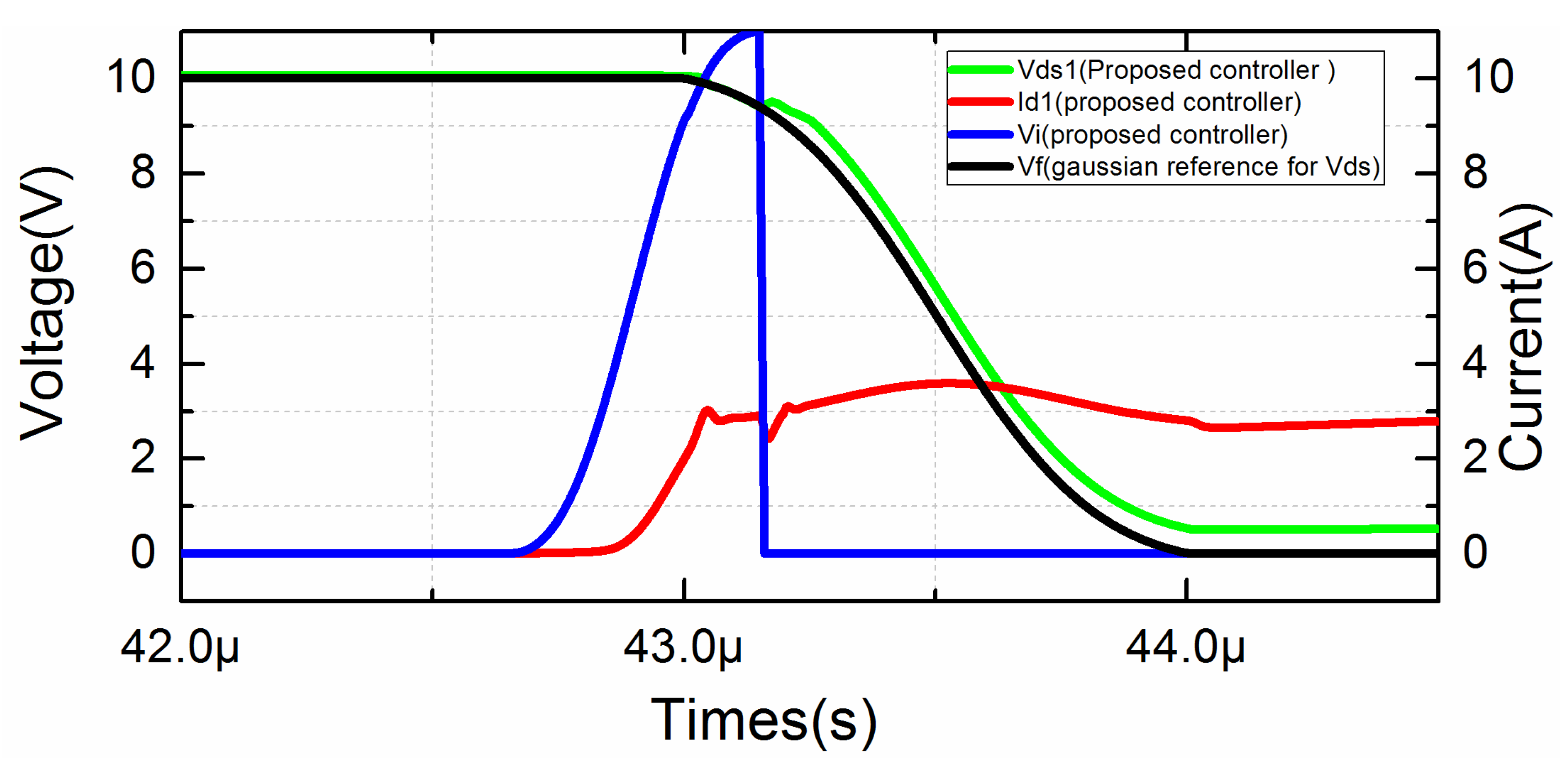
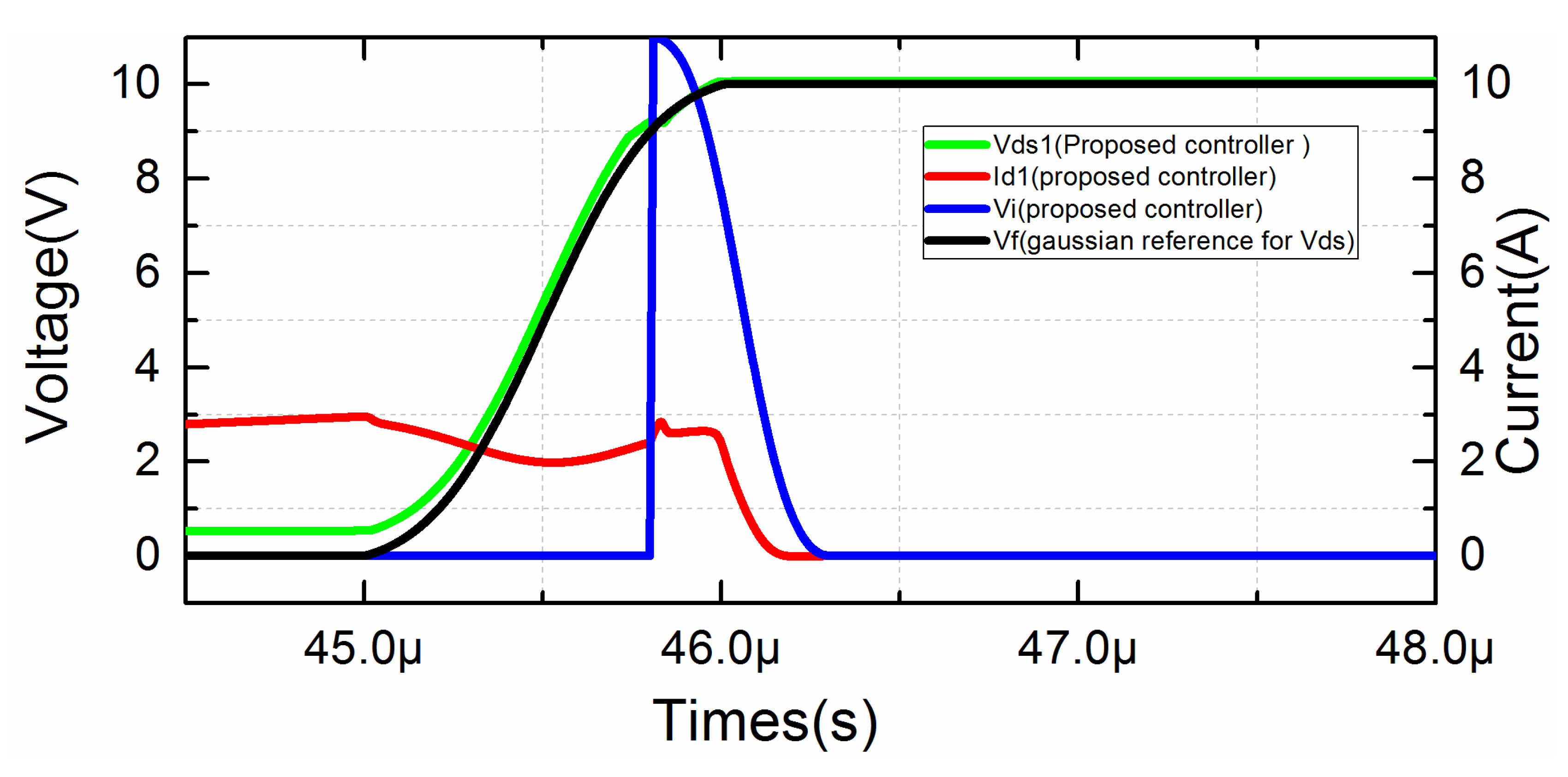
Before the experiment, it is necessary to simulate the proposed circuit, which can improve the experimental guidance and improve the efficiency for the experiment. Pspice is a professional circuit simulation software so it was chosen as the simulation software in this paper. Japan’s ROHM semiconductor’s SCT2160KE SiC MOSFET was selected and the body manufacturer offered the user a 1200-V/22-A Pspice model of SiC MOSFET. In order to simplify the circuit, the standard chopper unit was selected as the control object with inductive load in this paper. Both the voltage reference signal and the current control signal are Gaussian signals and the rising edge time, 1 µs, is equal to the falling edge time. The amplitudes of the voltage reference signal and the current control signal are 5, 4, respectively. According to Equation (11), the values of the Gaussian signal was calculated by the MATLAB and then imports into Pspice. The period is set to 6 µs and the duty cycle is 2/3. It is worth noting that in the simulation, the Gaussian reference signal is compared with the output signal that is fed back according to a certain ratio, rather than compared with the real output signal. Figure 9 and Figure 10 are simulation diagram for turn-on and turn-off in time domain respectively. The rising edge time and falling edge time of the voltage reference signal are both 1 µs and the rising edge time and falling edge time of the current control signal are also 1 µs in Figure 9 and Figure 10. The rising edge time and the falling edge time of the reference voltage are both 1 us, and the rising edge time rise time and the falling edge time of the current control voltage are both 0.5 µs. Figure 11 has the same working conditions with Figure 12 including the voltage reference signal and the current control signal. Comparing Figure 9, Figure 10, Figure 11 and Figure 12, it can be seen that the proposed method can not only achieve the output voltage following the reference voltage, but also control the rising and falling edge of the drain current. It is worth mentioning that due to the presence of the on-resistance and the sampling resistor, the minimum value of the output voltage Vds is not zero, and the minimum voltage of Vds is defined as VD1 in this paper.
where ID is the on-state current, Rin is on-state resistance and R3 is the sampling resistor.
VD1 = ID(Rin + R3),
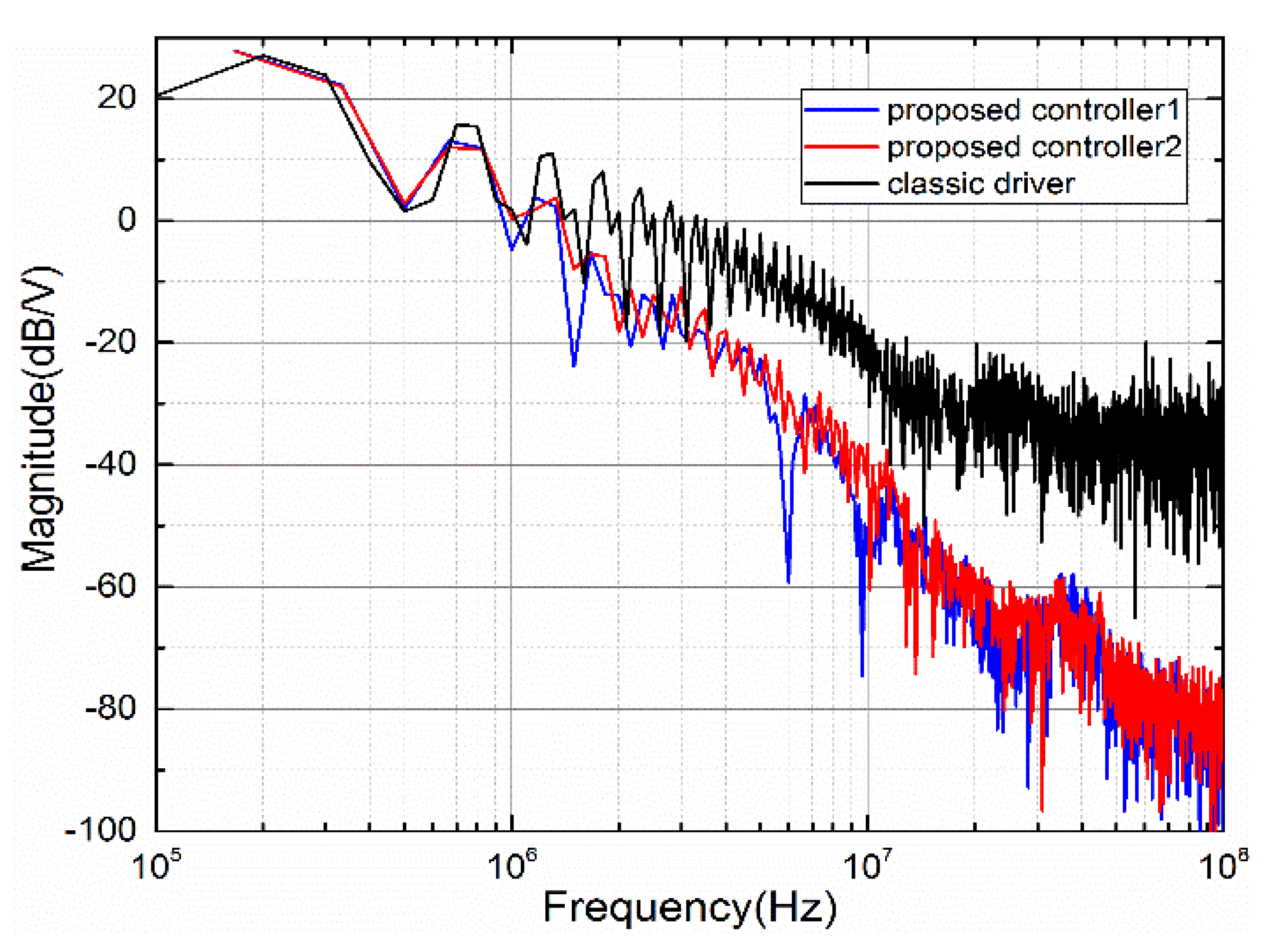
It is worth mentioning that the time domain diagrams of the gate-source voltage and gate current of the conventional gate drive method are also shown in Figure 9 and Figure 10. This paper compares the spectrum of the obtained drain voltage and drain current obtained by the conventional gate driving method and the proposed method shown in Figure 13 and Figure 14. Figure 13 shows the spectrum of the drain voltage obtained by the conventional method and the proposed method. It can be seen from Figure 13 that the envelope of the spectrum obtained by the proposed method is lower than the conventional gate driving method in the frequency range of 100 kHz to 70 MHz. However, the proposed method has obvious bumps in the spectrum around 80 M, which may be caused by fluctuations of the drain voltage caused by voltage switching. Figure 14 compared the spectrum of the drain current obtained by the proposed method with the drain current obtained by the conventional method. It can be seen from Figure 14 that when the frequency is less than 200 kHz, their spectral envelopes are basically coincident. When the frequency is higher than 200 kHz, the envelope obtained by the proposed method has a significant attenuation compared with the classical gate driving method and the attenuation is about 30 dB. Therefore, the effect of the proposed control method for suppressing EMI is very obvious.
5. Experiment Results of Proposed Method and Classic Method and Discussion
Similar to the simulation, the chopper unit with inductive load was also selected as the experimental circuit for simplicity. The op amp TH3091 that has wide Supply Range ±5 v to ±15 v, low voltage noise 2 nV and high band 200 MHz was used in this paper. The specific parameters of the proposed circuit and the classical gate drive circuit are listed in Table 1. The time domain data of the Gaussian signal is obtained by MATLAB and imported into the M3202A that is an arbitrary signal generator. The hardware configuration of the proposed intelligent control method is shown in Table 1. In the first experiment, proposed controller 1 was used, assuming that the rising edge time toff = 1 µs, the falling edge time tfall = 1 µs, cycle T = 6 µs, duty cycle D = 1/3 for the reference signal Vf and the rising edge time tr2 = 1 µs, the falling edge time tf2 = 1 µs for the control voltage Vi. The time domain relationship between voltage reference signal and current control signal is shown in Figure 6. In the second experiment, the proposed controller 2 was used, in which the setting of the voltage reference signal Vf was the same as the first experiment, but Vi, toff = 0.5 µs, tfall = 0.5 µs, is different with the first experiment.
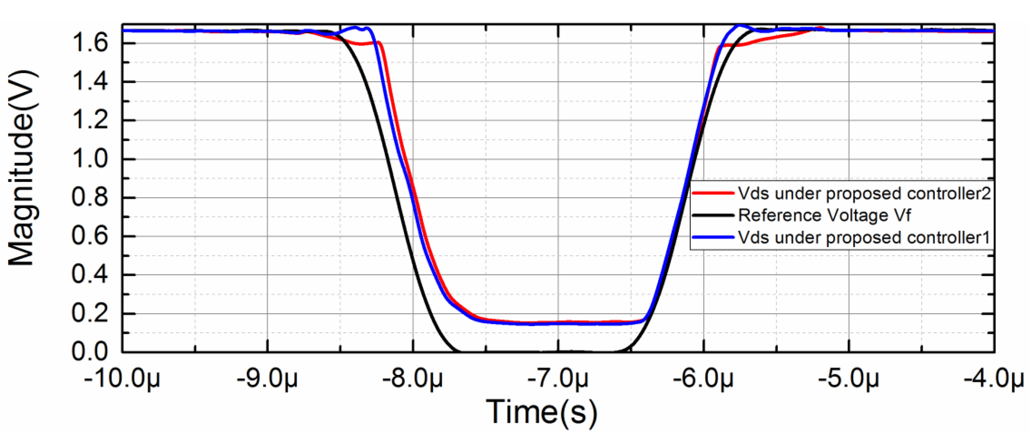
In Figure 15, the drain-source voltage Vds for the blue track of the controller 1 and the red track of controller 2 is delayed by 0.1 µs compared with the reference voltage at turn-on. At turn-off the drain-source voltage Vds for the blue track of the controller 1 and the red track of controller 2 follows the reference voltage well. However, for the blue trajectory and the red trajectory, there is a significant fluctuation in the top corner region at turn-on and turn-off, which may be caused by fluctuations in current for switching, parasitic inductance, and sampling resistor parasitic capacitance.
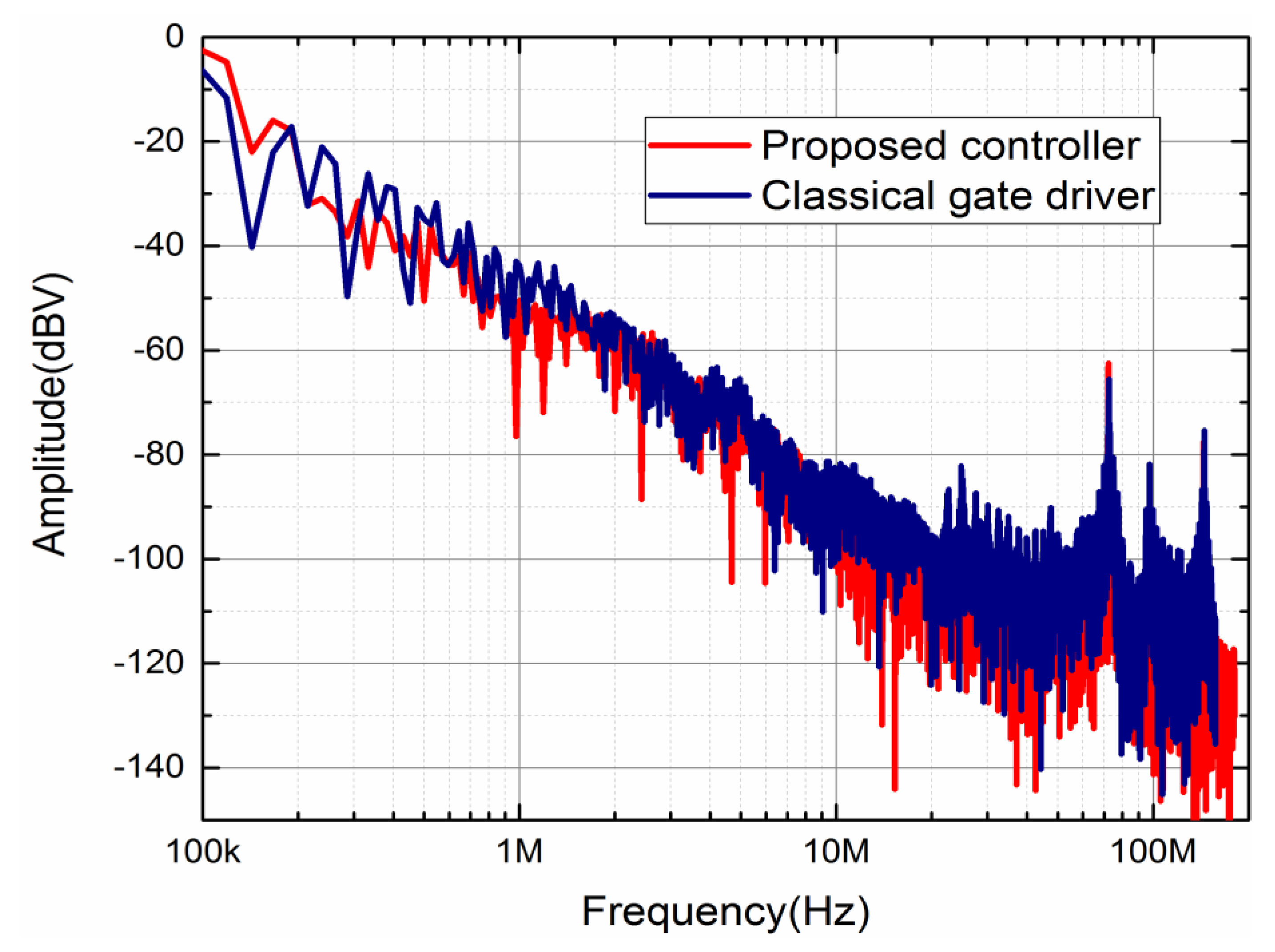
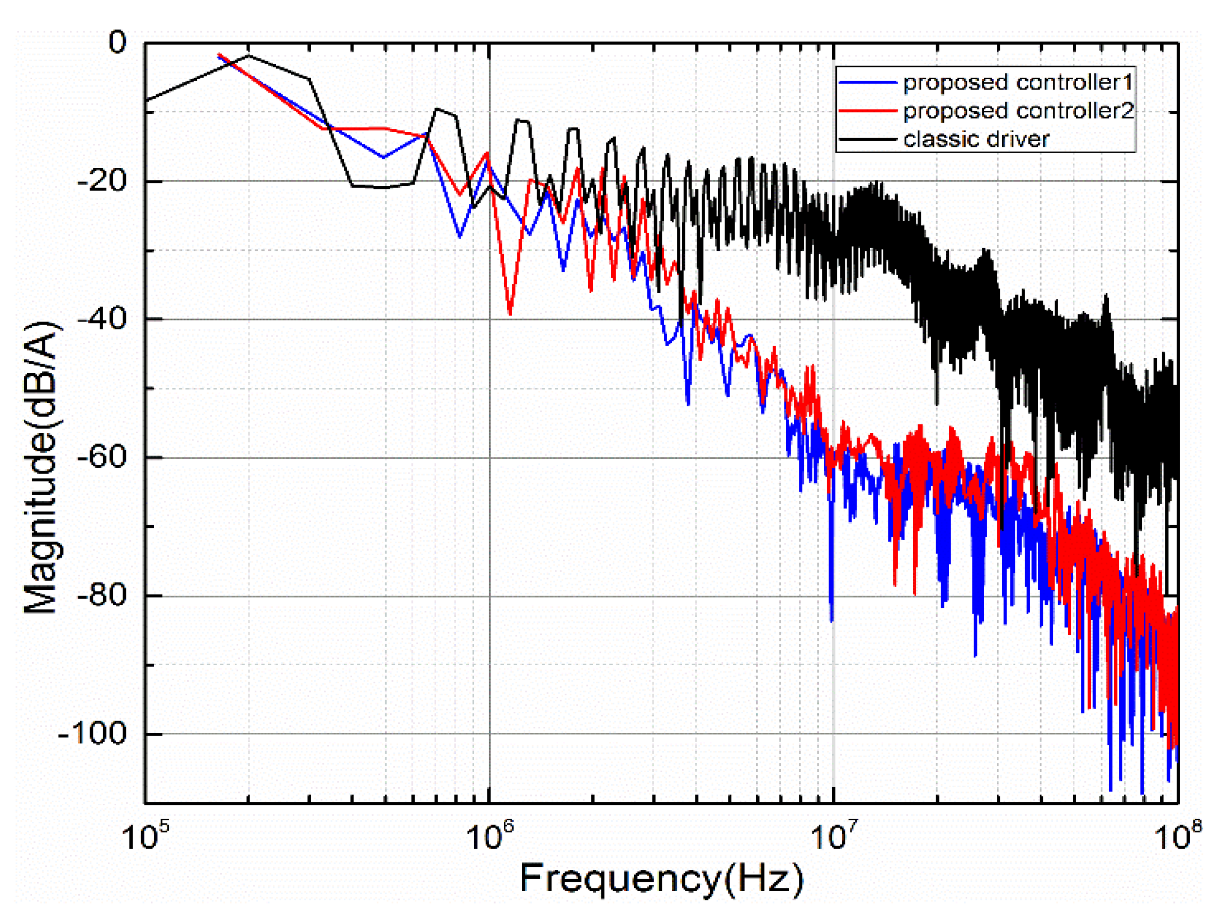
The classic gate driver is also used in the chopper for comparison, in which the hardware configuration is shown in Table 1 and the drive signal is the ideal PWM, the period 6 µs, duty cycle 1/3. The spectrum comparison of the drain-source voltage is shown in Figure 16. As can be seen from Figure 16, the envelopes of the three spectra in the low frequency region are almost coincident. The envelope of the classic gate drive in the 106–107 Hz range is 20 dB higher than the envelope of the proposed control 1 and control 2. The envelope of the classic gate drive in the range of 107–108 Hz is 40 dB higher than the proposed envelope of control 1 and control 2. In the analyzed frequency range of 105–108 Hz, the spectral envelopes of the proposed control 1 and control 2 are almost coincident, which shows that the current control signal Vi has little effect on the drain-source noise when the reference voltage Vf is the same in the proposed circuit.
In Figure 17, the drain current Id of proposed controller 1 has lower slope di/dt of 2.94 A/us than controller 2 of 6.46 A/us so that the controller 1 reduces the current overshoot 40% at turn-off. At turn-on, the switching speed di/dt of controller 1 is 4.58 A/us, and the di/dt of controller 2 is 6.87 A/us. Accordingly, the controller 1 reduces the current overshoot about 50%.
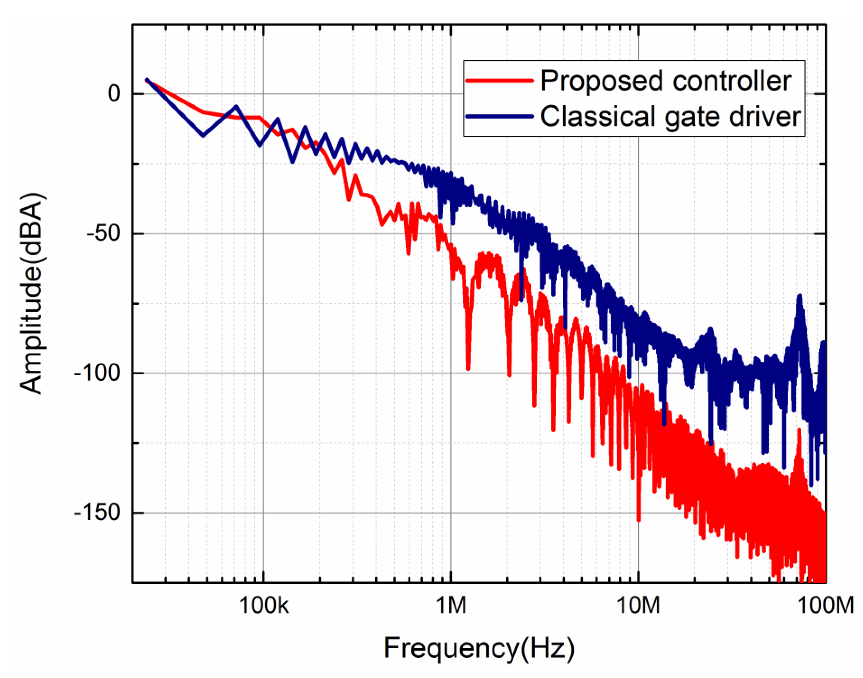
The spectrum comparison of the drain-source current Id is shown in Figure 18. It can be seen from the Figure 18 that before 3 × 10⁶ Hz, the spectrum of the classical gate driver, the proposed control 1 and control 2 are almost coincident. When the frequency is greater than 3 × 10⁶ Hz, the spectrum envelope of the classical gate driver is 10–40 dB higher than the proposed controller 1 and controller 2. In the frequency range of 107–5 × 10⁷ Hz, control 1 is reduced by 5–10 dB compared with controller 2, since the current slope di/dt of controller 1 is smaller than controller 2.
Switching losses also has been studied in this paper. The switching power of the three experiments are compared in Figure 19. As can be seen from Figure 19, there are mainly two peaks in one cycle. The first power peak is generated when the SiC MOSFET is turned on, and the second power peak is generated when the SiC MOSFET is turned off. The area enclosed by the power curve and the time axis represents the energy of the loss, and the loss at turn-on is higher than it at turn-off significantly. The typical gate driver switching losses are smaller than the proposed controller 1 and controller 2. Figure 20 shows the curve of switching loss over time in one cycle. It can be seen in Figure 20 that the proposed controller’s switching losses are approximately 120% higher than the classic gate drivers at the end of a cycle, since the switching time of the classic gate drive is much shorter than the proposed controller 1 and controller 2. The switching loss of the controller 2 is 6.4% lower than the controller 1, because the current rise and fall time of the controller 2 is shorter than the controller 1. It should be noted that in actual application, we can adjust the parameters to adjust the loss. According to [20], we know that there is compromise between EMI and switching losses. Therefore, we can reduce the switching loss by reducing the rising and falling edge times of the reference voltage within the acceptable EMI range.
6. Conclusions
The proposed intelligent control method has good EMI suppression for voltage and current compared with the classical gate driving method, the hard switching method. It has been proved that the intelligent control method can shape the SiC MOSFET switching transition effectively. Compared with the common method, it achieves control of drain-source voltage and drain current simultaneously. This method requires a precise fit of the voltage control signal and the current control signal so that a high frequency signal generator is needed. However, the proposed method needs longer switching time than classic driver so that the proposed method causes more power loss. Therefore, it is needed to tradeoff the EMI and switching loss. According to [20], it is an effective way to adjust the rise and fall switching time to reduce switching loss. Control signals can be obtained by convolution calculations and generated by high frequency multi-channel arbitrary signal generators. However, there are certain limitations, for example, voltage and current oscillations during circuit switching. The future work is to study the finite time stability of the circuit when two circuits work at the same time.
Author Contributions
Conceptualization, C.X. and Q.M.; Methodology, C.X.; Validation, C.X., Q.M., P.X. and C.T.; Investigation, C.X.; Writing—original draft preparation, C.X.; Writing—review and editing, C.X., Q.M., P.X. and C.T.
Funding
This research received no external funding.
Acknowledgments
The authors would like to thank Beihang University, Beijing, China for the financial support in executing this work successfully. This work has been carried out as a part of research work in the School of Automation Science and Electrical Engineering, Beihang University, Beijing, China.
Conflicts of Interest
The authors declare no conflict of interest.
References
- Costa, F.; Magnon, D. Graphical Analysis of the Spectra of EMI Sources in Power Electronics. IEEE Trans. Power Electron. 2005, 20, 1491–1498. [Google Scholar] [CrossRef]
- Yang, X.; Yuan, Y.; Zhang, X.; Palmer, P.R. Shaping High-power IGBT Switching Transitions by Active Voltage Control for Reduced EMI Generation. IEEE Trans. Ind. Appl. 2015, 51, 1669–1677. [Google Scholar] [CrossRef]
- Meng, J.; Ma, W.; Pan, Q.; Zhang, L.; Zhao, Z. Multiple slope switching waveform approximation to improve conducted EMI spectral analysis of power converters. IEEE Trans. Electromagn. Compat. 2006, 48, 742–751. [Google Scholar] [CrossRef]
- Idir, N.; Bausiére, R.; Franchaud, J.J. Active gate voltage control of turn-on di/dt and turn-off dv/dt in insulated gate transistors. IEEE Trans. Power Electron. 2006, 21, 849–855. [Google Scholar] [CrossRef]
- Chen, J. Design optimal built-in snubber in trench field plate power MOSFET for superior EMI and efficiency performance. In Proceedings of the 2015 International Conference on SISPAD, Washington, DC, USA, 9–11 September 2015; pp. 459–462. [Google Scholar]
- Palmer, P.R.; Rajamani, H.S. Active voltage control of IGBTs for high power applications. IEEE Trans. Power Electron. 2004, 19, 894–901. [Google Scholar] [CrossRef]
- Yang, X.; Zhang, X.; Palmer, P.R. IGBT converters conducted EMI analysis by controlled multiple-slope switching waveform approximation. In Proceedings of the IEEE ISIE, Taipei, Taiwan, 28–31 May 2013; pp. 1–6. [Google Scholar]
- Yang, X.; Zhang, X.; Zhang, J.; Palmer, P.R. Predictive optimisation of high-power IGBT switching under active voltage control. In Proceedings of the IECON 2013—39th Annual Conference of the IEEE Industrial Electronics Society, Vienna, Austria, 10–13 November 2013; pp. 1169–1174. [Google Scholar]
- Yang, X.; Palmer, P.R. Optimised IGBT turn-off under active voltage control in PEBB applications. In Proceedings of the 5th European Conference on Power Electronics and Applications (EPE), Lille, France, 2–6 September 2013; pp. 1–10. [Google Scholar]
- Wang, Z.; Shi, X.; Tolbert, L.M.; Blalock, B.J. Switching performance improvement of IGBT modules using an active gate driver. In Proceedings of the 28th Annual IEEE Applied Power Electronics Conference and Exposition (APEC), Long Beach, CA, USA, 17–21 March 2013; pp. 1266–1273. [Google Scholar]
- Witting, B.; Fuchs, F.W. Analysis and comparison of turnoff active gate control methods for low-voltage power MOSFETs with high current ratings. IEEE Trans. Power Electron. 2012, 27, 1632–1640. [Google Scholar] [CrossRef]
- Riazmontazer, H.; Rahnamaee, A.; Mojab, A.; Mehrnami, S.; Mazumder, S.K.; Zefran, M. Closed-loop control of switching transition of SiC MOSFETs. In Proceedings of the 2015 IEEE Applied Power Electronics Conf. and Exposition (APEC), Charlotte, NC, USA, 15–19 March 2015; pp. 782–788. [Google Scholar]
- Camacho, A.P.; Sala, V.; Ghorbani, H.; Martinez, J.L.R. A Novel Active Gate Driver for Improving SiC MOSFET Switching Trajectory. IEEE Trans. Ind. Electron. 2017, 64, 9032–9042. [Google Scholar] [CrossRef] [Green Version]
- Logsiger, Y.; Kolar, J.W. Closed-Loop di/dt and dv/dt IGBT Gate Driver. IEEE Trans. Power Electron. 2015, 30, 3402–3417. [Google Scholar]
- Oswald, N.; Stark, B.H.; Holliday, D.; Hargis, C.; Drury, B. Analysis of Shaped Pulse Transitions in Power Electronic Switching Waveforms for Reduced EMI Generation. IEEE Trans. Ind. Appl. 2011, 47, 2154–2165. [Google Scholar] [CrossRef]
- Cui, T.K.; Ma, Q.S.; Xu, P.; Wang, Y.C. Analysis and Optimization of Power MOSFETs Shaped Switching Transients for Reduced EMI Generation. IEEE Access 2017, 5, 20440–20448. [Google Scholar] [CrossRef]
- Patin, N.; Vinals, M.L. Toward an optimal Heisenberg’s closed-loop gate drive for power MOSFETs. In Proceedings of the IECON 2012—38th Annual Conference on IEEE Industrial Electronics Society, Montreal, QC, Canada, 25–28 October 2012; pp. 828–833. [Google Scholar]
- Xu, C.W.; Ma, Q.S.; Xu, P.; Cui, T.K.; Zhang, P.M. An Improved Active Gate Drive Method for SiC MOSFET Better Switching Performance. In Proceedings of the 2018 IEEE 3rd Advanced Information Technology, Electronic and Automation Control Conference (IAEAC), Chongqing, China, 12–14 October 2018. [Google Scholar]
- Wang, J.J.; Chung, H.S.H.; Li, R.T.H. Characterization and Experimental Assessment of the Effects of Parasitic Elements on the MOSFET Switching Performance. IEEE Trans. Power Electron. 2013, 28, 573–590. [Google Scholar] [CrossRef]
- Oswald, N.; Anthony, P.; McNeill, N.; Stark, B.H. An Experimental Investigation of the Tradeoff between Switching Losses and EMI Generation With Hard-Switched All-Si, Si-SiC, and All-SiC Device Combinations. IEEE Trans. Power Electron. 2014, 29, 2393–2407. [Google Scholar] [CrossRef]
Figure 1.
Switching signal (a) and structure (b).

Figure 2.
Spectra comparison of zero-order waveform (square signal), one-order waveform (trapezoidal signal) and infinite-order waveform (Gaussian signal).
Figure 2.
Spectra comparison of zero-order waveform (square signal), one-order waveform (trapezoidal signal) and infinite-order waveform (Gaussian signal).

Figure 3.
The general scheme of control method for the proposed time division shaped switching transitions.
Figure 3.
The general scheme of control method for the proposed time division shaped switching transitions.

Figure 4.
Turn-on voltage and current of SiC MOSFET under hard switching conditions.

Figure 5.
Turn-off voltage and current of SiC MOSFET under hard switching conditions.

Figure 6.
Time domain diagram of Gaussian control signals for voltage and current.

Figure 7.
Turn-on voltage and current waveform of SiC MOSFET the in the proposed circuit.

Figure 8.
Turn-off voltage and current waveform of SiC MOSFET in the proposed circuit.

Figure 9.
Pspice simulation for SiC MOSFET during turn-on with 1 µs falling edge of Vf (reference voltage) and 1 µs rising edge of Vi (the voltage to control current).
Figure 9.
Pspice simulation for SiC MOSFET during turn-on with 1 µs falling edge of Vf (reference voltage) and 1 µs rising edge of Vi (the voltage to control current).

Figure 10.
Pspice simulation for SiC MOSFET during turn-off with 1 µs rising edge time of Vf (reference voltage) and 1 µs falling edge time of Vi (the voltage to control current).
Figure 10.
Pspice simulation for SiC MOSFET during turn-off with 1 µs rising edge time of Vf (reference voltage) and 1 µs falling edge time of Vi (the voltage to control current).

Figure 11.
Pspice simulation SiC MOSFET during turn-on with 1 µs falling edge time of Vf (reference voltage) and 0.5 µs rising edge time of Vi (the voltage to control current).
Figure 11.
Pspice simulation SiC MOSFET during turn-on with 1 µs falling edge time of Vf (reference voltage) and 0.5 µs rising edge time of Vi (the voltage to control current).

Figure 12.
Pspice simulation SiC MOSFET during turn-off with 1 µs decline time of Vf and 0.5 µs rise time of Vi.
Figure 12.
Pspice simulation SiC MOSFET during turn-off with 1 µs decline time of Vf and 0.5 µs rise time of Vi.

Figure 13.
Pspice simulation Vds spectra comparison (toff = tfall = 1.0 µs, purple: classic gate driver, red: proposed controller).
Figure 13.
Pspice simulation Vds spectra comparison (toff = tfall = 1.0 µs, purple: classic gate driver, red: proposed controller).

Figure 14.
Pspice simulation Id spectra comparison (toff = tfall = 1.0 µs, purple: classic gate driver, red: proposed controller).
Figure 14.
Pspice simulation Id spectra comparison (toff = tfall = 1.0 µs, purple: classic gate driver, red: proposed controller).

Figure 15.
Experiment result that voltage comparison Vds of proposed controller 1 (blue, toff = tfall = 1 µs of Vf), proposed controller 2 (red, toff = tfall = 1 µs of Vf), and reference voltage Vf (black, toff = tfall = 1 µs).
Figure 15.
Experiment result that voltage comparison Vds of proposed controller 1 (blue, toff = tfall = 1 µs of Vf), proposed controller 2 (red, toff = tfall = 1 µs of Vf), and reference voltage Vf (black, toff = tfall = 1 µs).

Figure 16.
Spectra comparison of Vds between classic gate driver (black), proposed controller 1 (blue) and proposed controller 2 (red). Same reference voltage Vf was used in controller 1 and controller 2.
Figure 16.
Spectra comparison of Vds between classic gate driver (black), proposed controller 1 (blue) and proposed controller 2 (red). Same reference voltage Vf was used in controller 1 and controller 2.

Figure 17.
Experiment results of Id for turn-on and off transition between controller 1 (toff = tfall = 1 µs of Vi) and controller 2 (toff = tfall = 0.5 µs of Vi). Same reference voltage Vf was used in controller 1 and controller 2.
Figure 17.
Experiment results of Id for turn-on and off transition between controller 1 (toff = tfall = 1 µs of Vi) and controller 2 (toff = tfall = 0.5 µs of Vi). Same reference voltage Vf was used in controller 1 and controller 2.

Figure 18.
Spectra comparison for Id between classic gate driver (black), proposed controller 1 (blue) and proposed controller 2 (red).
Figure 18.
Spectra comparison for Id between classic gate driver (black), proposed controller 1 (blue) and proposed controller 2 (red).

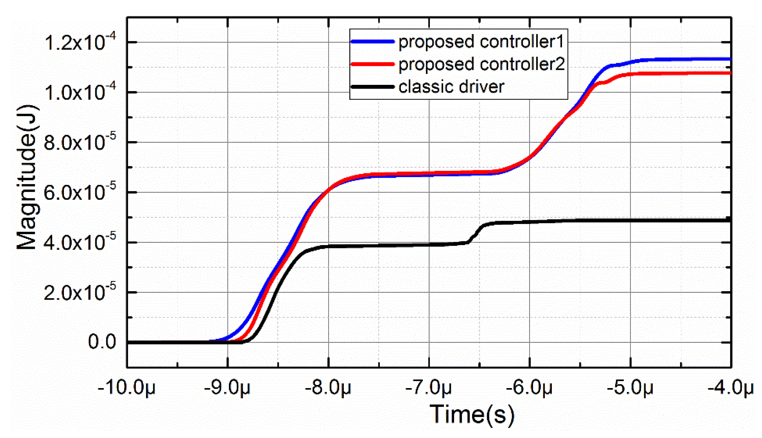
Figure 19.
Power comparison between the proposed controller 1, the proposed controller 2, and classical gate driver.
Figure 19.
Power comparison between the proposed controller 1, the proposed controller 2, and classical gate driver.

Figure 20.
Switching losses comparison between the proposed controller 1, the proposed controller 2, and classical gate driver.
Figure 20.
Switching losses comparison between the proposed controller 1, the proposed controller 2, and classical gate driver.


Table 1.
Experiment circuit parameters.
| Rg(Ω) | Op Amp | A1 × A2 | Driver | |
|---|---|---|---|---|
| Classical gate driver | 5 | NULL | NULL | MOS |
| Proposed Intelligent controller | 5 | THS3091 | 10 × 1 | MOS |
© 2019 by the authors. Licensee MDPI, Basel, Switzerland. This article is an open access article distributed under the terms and conditions of the Creative Commons Attribution (CC BY) license (http://creativecommons.org/licenses/by/4.0/).
Share and Cite
MDPI and ACS Style
Xu, C.; Ma, Q.; Xu, P.; Cui, T. Shaping SiC MOSFET Voltage and Current Transitions by Intelligent Control for Reduced EMI Generation. Electronics 2019, 8, 508. https://doi.org/10.3390/electronics8050508
AMA Style
Xu C, Ma Q, Xu P, Cui T. Shaping SiC MOSFET Voltage and Current Transitions by Intelligent Control for Reduced EMI Generation. Electronics. 2019; 8(5):508. https://doi.org/10.3390/electronics8050508
Chicago/Turabian StyleXu, Congwen, Qishuang Ma, Ping Xu, and Tongkai Cui. 2019. "Shaping SiC MOSFET Voltage and Current Transitions by Intelligent Control for Reduced EMI Generation" Electronics 8, no. 5: 508. https://doi.org/10.3390/electronics8050508
Note that from the first issue of 2016, this journal uses article numbers instead of page numbers. See further details here.