A Novel Single-switch Phase Controlled Wireless Power Transfer System


1
Key Laboratory of Control of Power Transmission and Transformation Ministry of Education, Shanghai Jiao Tong University, 800 Dongchuan RD., Shanghai 200240, China
2
College of Electric and Information Engineering, Zhengzhou University of Light Industry, Zhengzhou 450002, China
*
Author to whom correspondence should be addressed.
Electronics 2018, 7(11), 281; https://doi.org/10.3390/electronics7110281
Submission received: 6 October 2018
/
Revised: 22 October 2018
/
Accepted: 25 October 2018
/
Published: 29 October 2018
(This article belongs to the Special Issue Applications of Power Electronics)
Abstract
:Battery charging is a fundamental application of Wireless Power Transfer (WPT) systems that requires effective implementation of Constant Current (CC) and Constant Voltage (CV) power conduction modes. DC-DC converters used in WPT systems utilize large inductors and capacitors that increase the size and volume of the system in addition to causing higher DC losses. This work proposes a novel single-switch active rectifier for phase controlled WPT systems that is smaller in volume and weight as compared to conventional WPT topologies. The proposed method simplifies the control scheme using improved Digital Phase Control (DPC) and Analog Phase Control (APC) to realize the CC and CV power transfer modes. Furthermore, it prevents forward voltage losses in Silicon Carbide (SiC) switches and shoot through states with improved switching patterns. Simulation studies and experimental results are added to verify the effectiveness of the proposed methodology.
1. Introduction
WPT techniques can realize energy conversion without physical connections. It has gained tremendous attention in both research and industry. Recently, wireless charging is the focus of study. To improve battery life time, the system has special requirements for the charging current and voltage profiles. WPT systems can realize both CC and CV power transfer modes through either primary or secondary side control. However, primary side control requires an additional communication channel [1,2]. It is more simplified and straightforward to directly achieve the CC and CV power transfer modes through secondary side control. Therefore, various DC-DC converters [3,4,5,6,7,8] are installed on the receiver side for power regulation, including buck converter [4], boost converter [5,9,10], and buck-boost converter [6,11]. Although DC-DC converters have simpler controls, they require additional capacitors and inductors that increase the weight, volume, and cost of the receiver. In addition, more cascaded circuits result in more losses on the DC side. To address these drawbacks, researchers propose active rectifiers on the receiver side. Active rectifiers are initially put forward to reduce the conduction losses of the diode rectifier and transfer the power bi-directionally [12,13,14,15,16,17,18,19]. Recently, Phase Control (PC) method is introduced to regulate resonant currents [20,21,22,23,24,25], which can further reduce the energy consumed by parasitic resistances.
Active rectifiers proposed for WPT systems can be classified into three categories: (i) full bridge rectifier with four switches; (ii) semi-bridgeless rectifier with two switches; and (iii) single-switch rectifier. Full active bridge rectifiers are used in various applications [12,13,14,15,16,17,18,19,20,21,22,23,24,25]. Four Metal-Oxide-Semiconductor Field Effect Transistors (MOSFETs) and four isolated driver circuits are installed on the receiver side. Short circuit may appear in the full bridge topology due to faulty operation. Such a characteristic reduces the reliability of the WPT systems, especially battery charging systems where short circuit can lead to fire and explosion. It is desirable to investigate a more cost-effective and reliable approach to achieve secondary PC. Therefore, researchers in [26,27,28] develop two-switch rectifiers for WPT systems. In [26,27], a semi-bridgeless topology with two MOSFETs is proposed, where two switches are installed on the lower side of the rectifier. Secondary PC can be achieved as well. In [28], two MOSFETs are in reverse connection and controlled by one signal. Duty ratio control is applied to regulate the power. Furthermore, researchers in [29,30,31,32,33,34,35,36] investigate single-switch rectifiers. In [29], a switch is connected in parallel with a resonant compensation capacitor. Power regulation can be achieved by tuning/detuning through this variable capacitor. However, this method makes the system deviate from optimal resonant point, which may cause an efficiency drop. In [30,31,32], a switch is connected in series with parallel resonant tank. When the switch is turned off, the receiver transfers the power only in half the period. In addition, it is difficult to obtain a stable DC voltage. In [33], an active switch is inserted into the lower phase leg of a full diode bridge. When the switch is turned on, the resonant tank is shorted in half the period and the power can be regulated by duty ratio control. In [34,35,36], a boost converter is directly connected after the diode bridge which reduces one filter capacitor.
Active rectifiers with two or four switches can realize PC [12,13,14,15,16,17,18,19,20,21,22,23,24,25,26,27], whereas previous single-switch rectifiers can only adopt duty ratio control [29,30,31,32,33,34,35,36]. Although duty ratio control is easier to implement, it can cause resonant current oscillations when the power transfer path is chopped. It requires larger filter capacitors to maintain the desired DC voltage. In addition, single-switch receivers in [29,30,31,32,33] are half-controlled, i.e., their power regulation abilities are restricted, which may fail to meet the CC and CV power transfer requirements.
This paper proposes a novel single-switch phase controlled receiver for WPT systems for the first time. With this method, the secondary side inductor is removed and only a small filter capacitor is added, thereby reducing the size of the receiver and lessening the number of switches used. The salient contributions of this work are:
- (1)
- The proposed methodology reduces the number of active switches and isolated driver circuits as compared to conventional phase controlled receivers.
- (2)
- An APC method is applied to this improved receiver that circumvents synchronization algorithms and additional programming. APC method regulates the power automatically, which reduces the difficulty in design and implementation.
- (3)
- Most previously discussed single-switch methods are half-controlled and use duty ratio variation. In this work, the receiver is fully controlled and has a stronger power regulation ability as compared to conventional single-switch receivers.
- (4)
- The proposed receiver fully utilizes the SiC MOSFET to reduce switching losses while avoiding high forward voltage losses through its intrinsic diode.
This paper is divided as follows: Section 2 shows the proposed single-switch receiver and illustrates its operating modes. Then, it presents the derivations for the CC and CV power transfer modes. Section 3 elaborates the detailed implementation techniques of the proposed DPC and APC methods. In Section 4, simulations and experiments are added to validate the feasibility and effectiveness of the proposed topology and control methods. Finally, Section 5 concludes this paper.
2. Modeling and Analysis
This section presents mathematical modeling and analysis for the proposed WPT system.
2.1. Proposed Topology
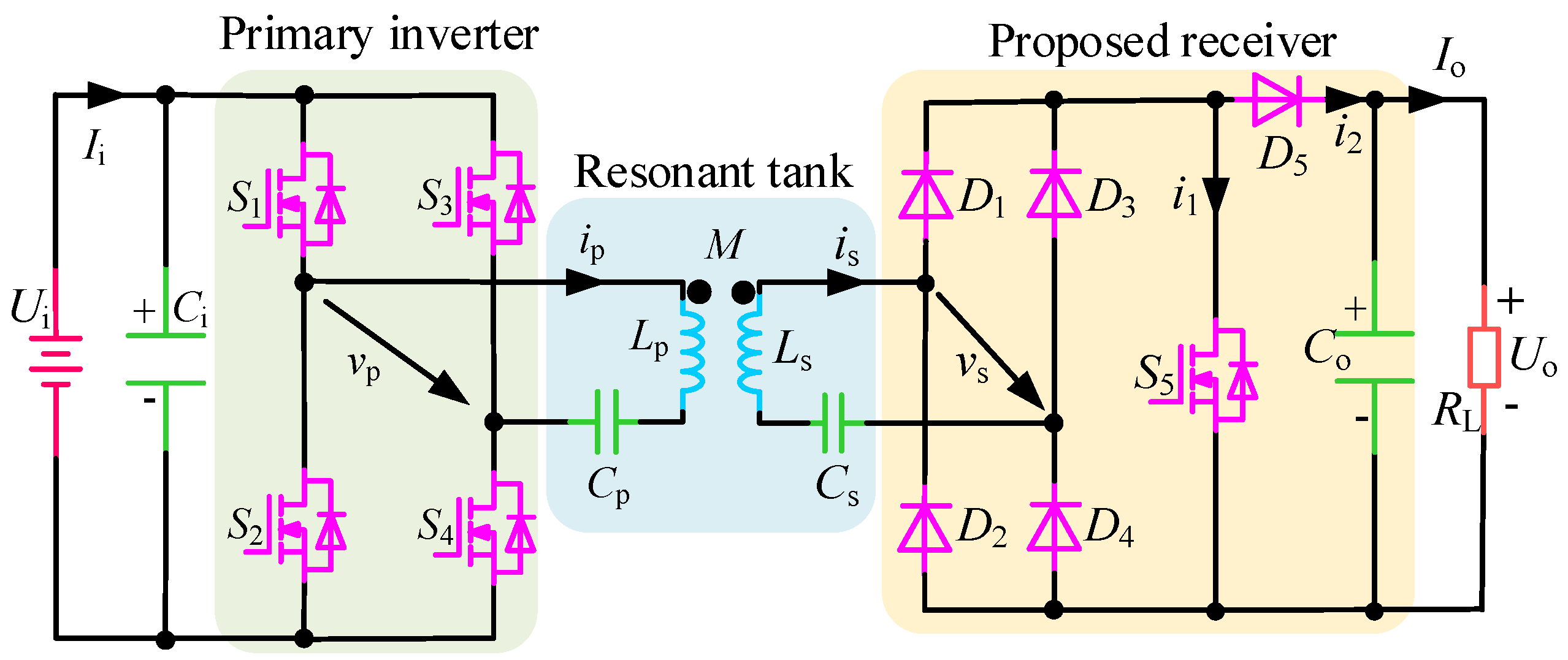
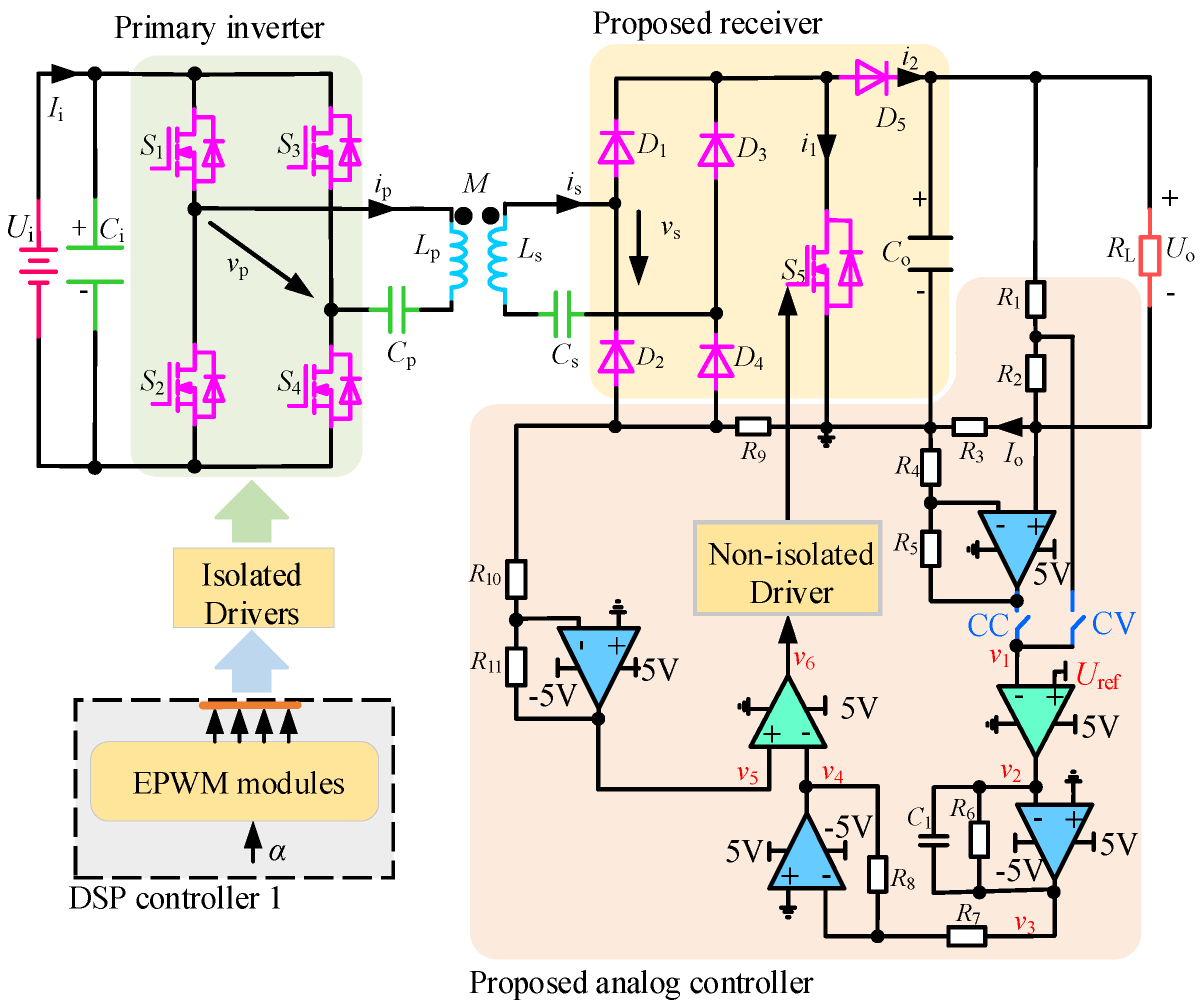
A WPT system with the proposed single-switch receiver is shown in Figure 1. Ui and Uo are the DC voltages, whereas vp and vs are the primary and secondary resonant voltages. Lp and Ls are the primary and secondary coil inductances, which are compensated by Cp and Cs, respectively. S1–S5 are the SiC MOSFETs, and D1–D5 are the diodes. Ci and Co are the filter capacitors, and RL is the load. i1 and i2 are the currents flowing through S5 and D5, respectively. Ii and Io denote the input and output DC currents.
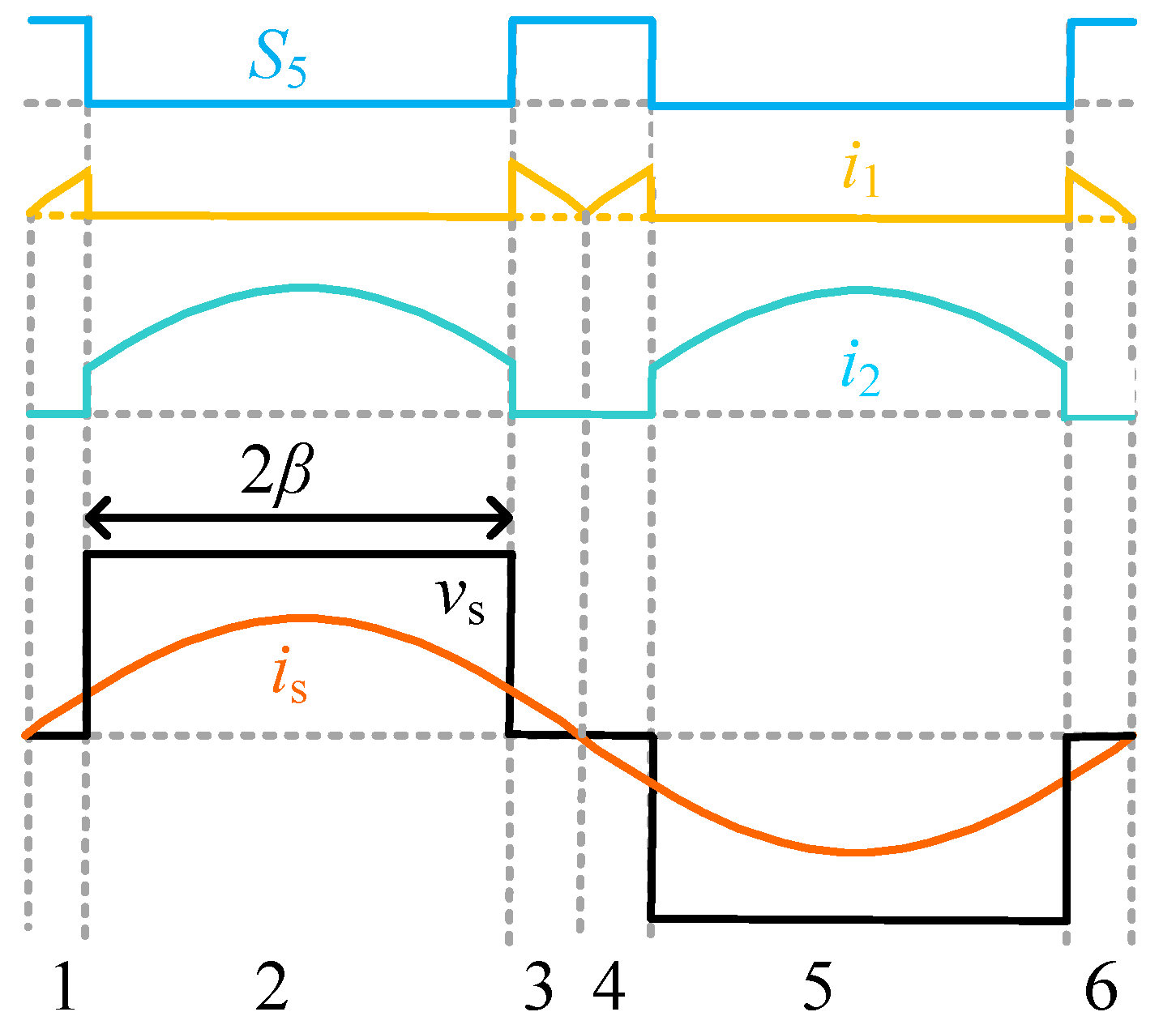
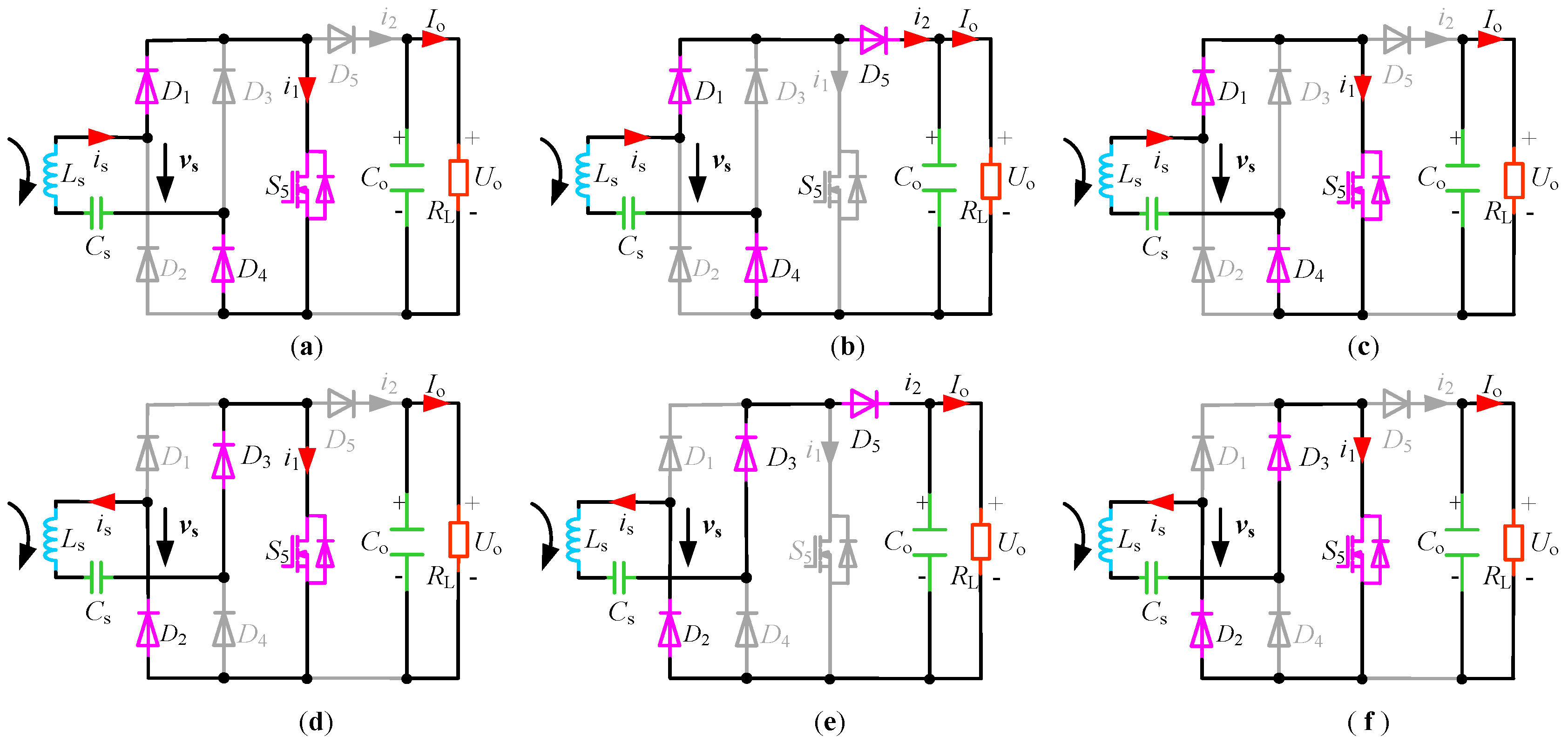
The typical waveforms of the proposed topology are shown in Figure 2, where 2β presents the phase angle of vs. According to the current directions and paths, the receiver has six operating modes as depicted in Figure 3.
Mode 1: is > 0, and S5 is on. There exist two current loops on the receiver side: Ls–D1–S5–D4–Cs and Co–RL. The diode bridge is short-circuited by S5, and Io is supplied by Co. Thus, vs is zero.
Mode 2: is > 0, and S5 is turned off at the beginning of Mode 2. Co charges, and Uo increases. Thus, the current loop is Ls–D1–D5–Uo–D4–Cs. vs is basically equal to Uo.
Mode 3: is > 0, and S5 is turned on at the beginning of Mode 3. Then, is flows through S5 and vs becomes zero. Uo is supplied by Co, and it begins to decrease. The current loops are: Ls–D1–S5–D4–Cs and Co–RL.
Mode 4: S5 remains on and vs. remains zero, whereas is changes its direction. Uo continues to decrease. The current loop of is becomes Ls–Cs–D3–S5–D2.
Mode 5: is < 0, and S5 is turned off at the beginning of Mode 5. Co charges via is, and Uo begins to increase. The current loop is Ls–Cs–D3–D5–Uo–D2. vs is basically equal to −Uo.
Mode 6: is < 0, and S5 is turned on at the beginning of Mode 6. The current loop of is becomes Ls–Cs–D3–S5–D2, and Uo is supplied by Co again.
To minimize switching losses, a SiC MOSFET can be used. Since the forward voltage of the intrinsic diode of the SiC MOSFET is high, a SiC diode is connected in parallel to overcome the high forward voltage loss of the intrinsic diode. However, no current freewheels through S5 in the proposed receiver, which means the SiC diode is not necessary in this application. Therefore, the proposed receiver can fully utilize the SiC MOSFET to reduce switching losses while avoiding its drawback of high forward voltage losses through its intrinsic diode.
2.2. Power Regulation
The CC and CV power transfer realizations are the basic requirements for battery charging systems. This section presents the theoretical analysis of secondary side control through proposed single-switch phase-controlled receiver.
The system operates at the resonant frequency, that is
Rp and Rs represent primary and secondary coil resistances, respectively. Then, the following equations are obtained according to Kirchhoff Voltage Law (KVL).
According to Fourier series and fundamental harmonic analysis [23,24,25], the root-mean-square value of vs (Vs) can be denoted as:
Without considering the switching losses, the input and output powers of the rectifier are equal.
Then, Io versus Is is deduced.
According to Equation (2), is can be rewritten as
Thus, Io and Uo can be approximately derived as Equations (8) and (9).
A larger β means a larger Io and Uo. Therefore, β can be utilized to achieve the CC and CV power transfer modes.
3. Implementation Methods
This section presents implementation techniques for realizing DPC and APC with the proposed receiver in WPT system.
3.1. Digital Phase Control
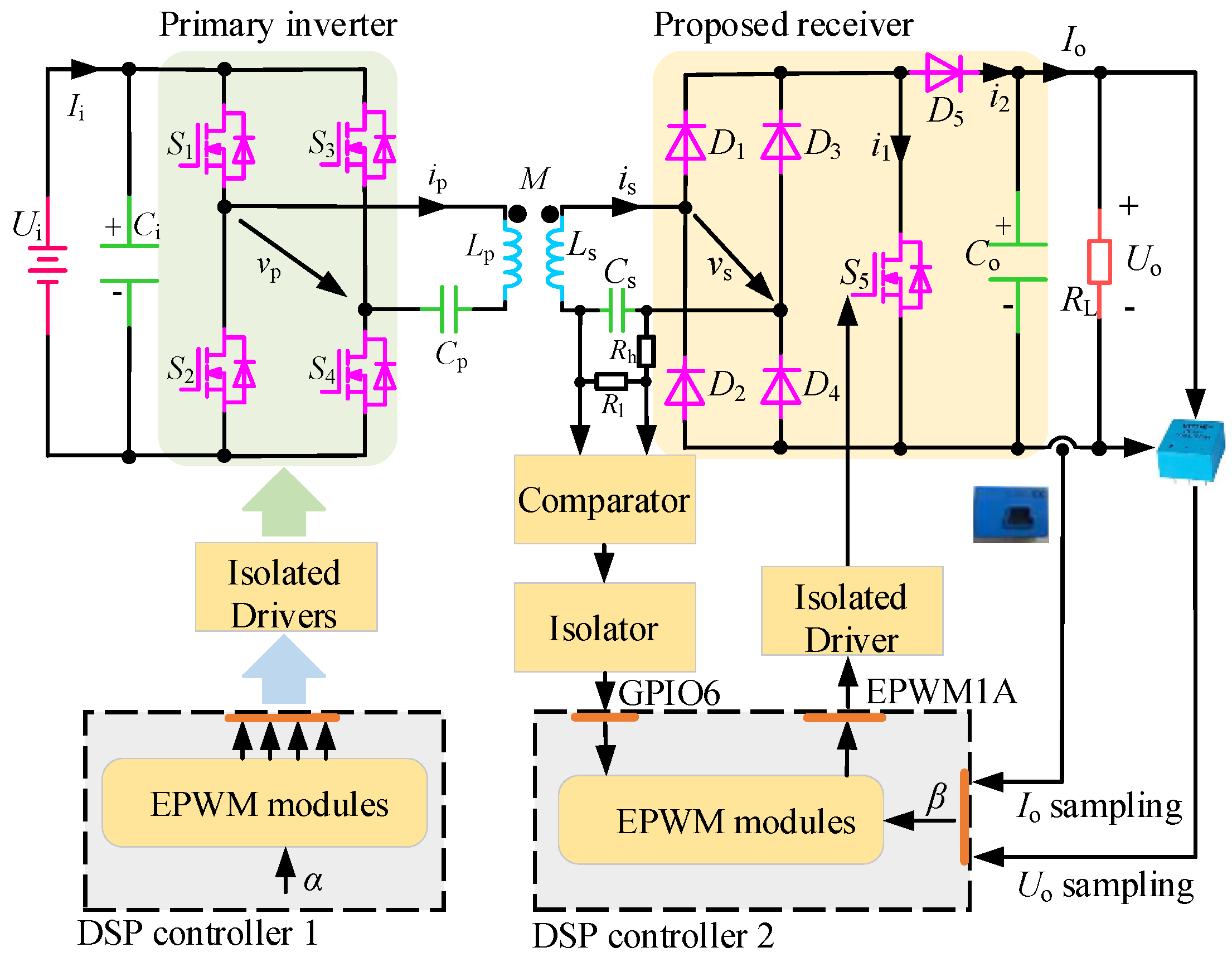
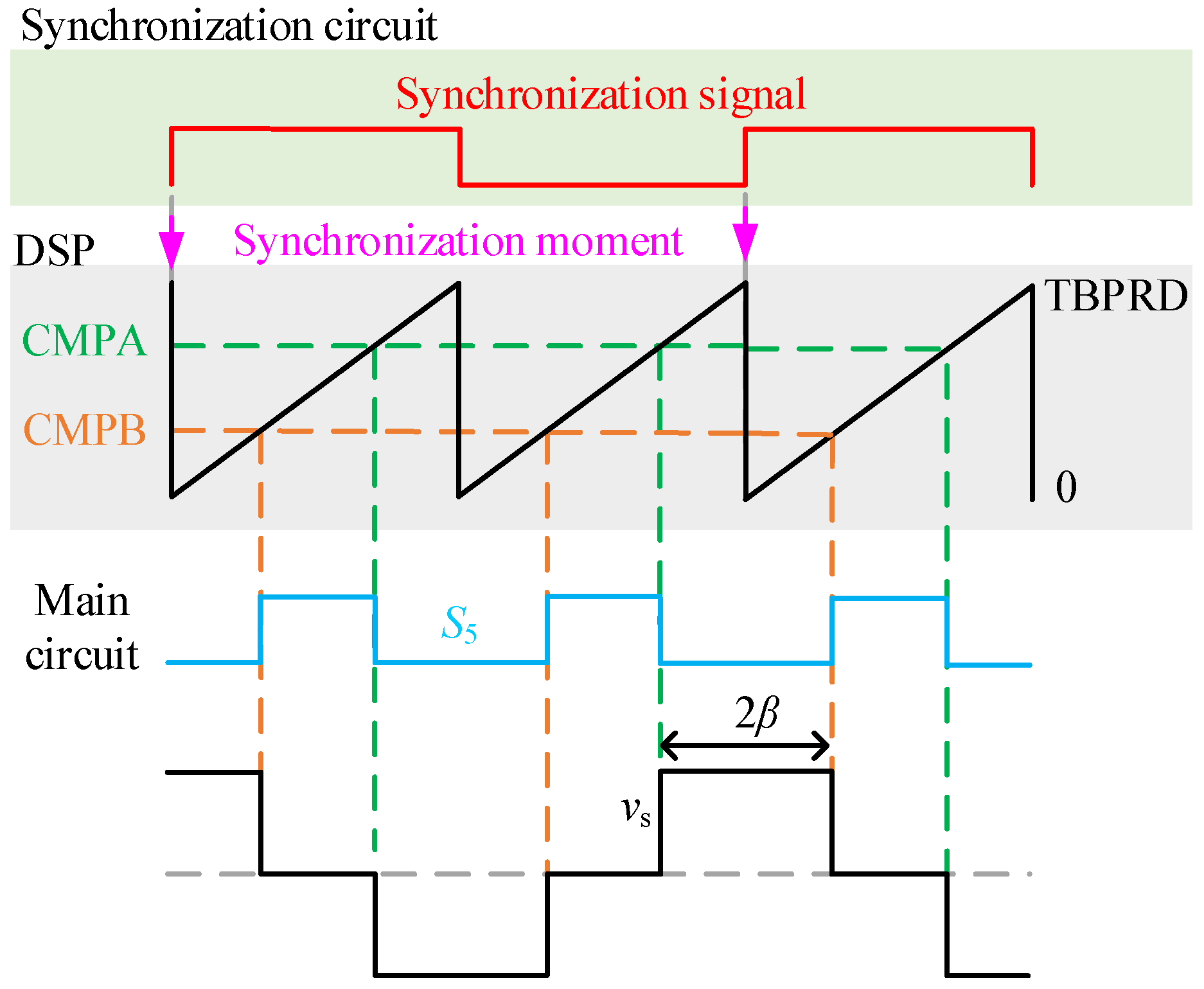
The schematic of the DPC system is shown in Figure 4, where two independent Digital Signal Processors (DSPs) are installed. Digital control is widely used for various applications due to its flexibility. Since the controller should be isolated from the main circuit for safety consideration, isolated driver circuits as well as isolated power supplies are installed on primary and secondary sides. Furthermore, isolated current and voltage sensors are required on the receiver side for output electrical information feedback. To avoid power oscillations, the synchronization of secondary receiver is of essential importance. In [24], secondary synchronization is realized by utilizing the resonant voltage across Cs. The synchronization circuit consists of a comparator and an isolator, as shown in Figure 4, where Rh and Rl are the divider resistances. The operating frequency of the receiver-side switches in the full active bridge is equal to the current frequency, whereas it is twice that frequency in the proposed receiver. Thus, the receiver is synchronized once every two periods.
Figure 5 shows the typical synchronization waveforms. The comparator turns the divided sinusoidal voltage into a square-wave synchronization signal. After passing a digital isolator, it is sent to the synchronization port of the DSP controller. TBPRD, CMPA, and CMPB are the time base period and comparing values of the reserved registers of the controller, respectively. The 0 and TBPRD shown in Figure 5 are the minimum and maximum values of the counter of the controller, i.e., CMPA and CMPB fall within the range of [0, TBPRD]. When the counter reaches CMPA, S5 is turned off. When the counter reaches CMPB, S5 is turned on. The relationships among TBPRD, CMPA, CMPB, and β are shown in Equations (10) and (11).
TBPRD is determined by the inverter frequency, and the comparing values produce the desired β. Afterwards, the corresponding gate drive signal generates vs in the main circuit.
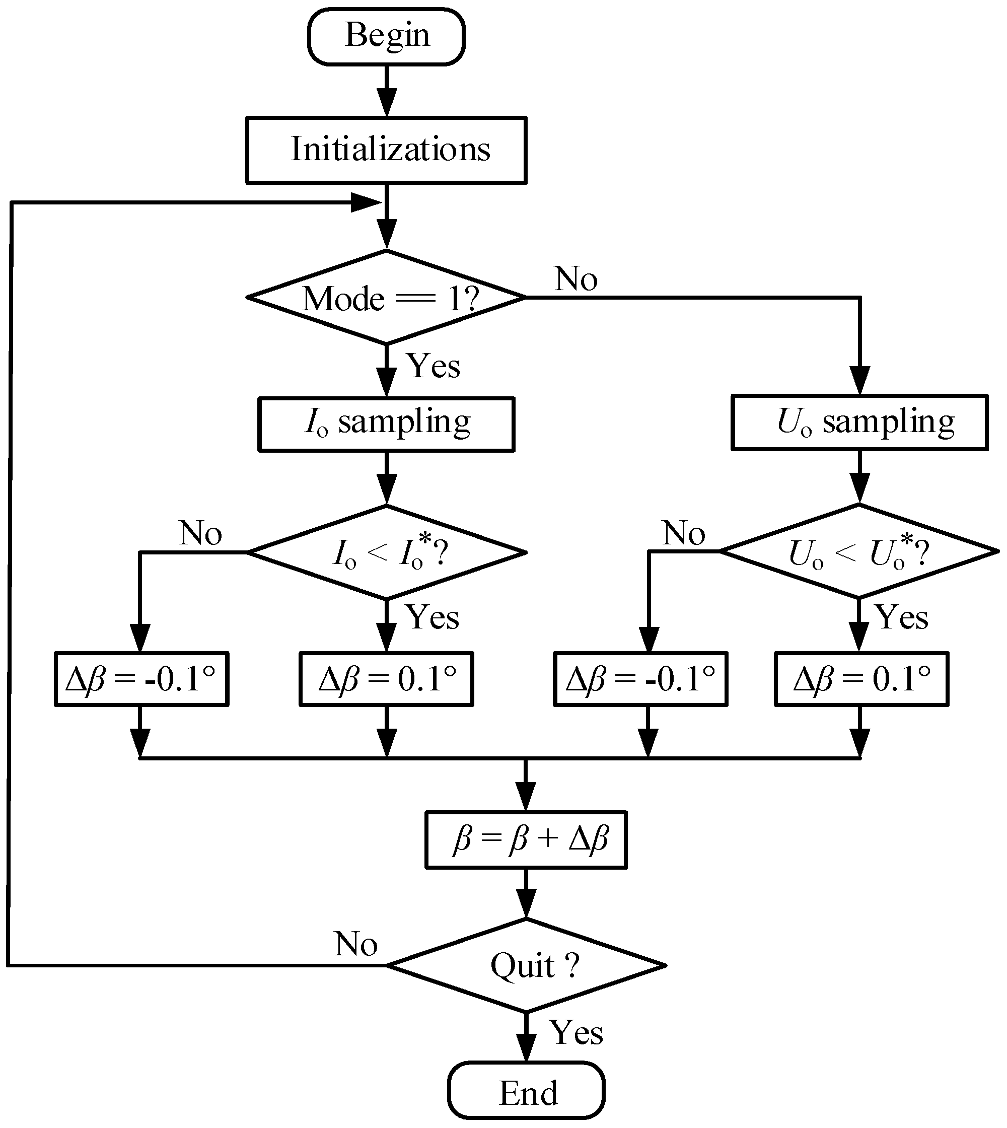
As analyzed in Section 2, a larger β brings about larger Io and Uo. Therefore, the output power regulation can be achieved by changing β. The algorithm flowchart of the CC and CV power transfer modes is shown in Figure 6, where and are the expected current and voltage values. Power transfer mode selection is determined by one bit, referred to as “Mode”, which is defined in the controller. The designer can initialize the Mode by setting it at 1 or 0 in the software code. When the Mode is 1, the receiver operates at the CC power transfer mode, otherwise, it operates at the CV power transfer mode. Io is sampled for the CC power transfer mode, and Uo for the CV power transfer mode. To obtain accurate sampling values, 20 samplings of Io or Uo are averaged. β ranges from 0° to 90°. When Io or Uo is smaller than the desired value, β is increased by 0.1°. Otherwise, β is decreased by 0.1°. This control algorithm is simple and effective. The primary controller is turned on and the primary active bridge inverts the high frequency voltage. The frequency locking signal is generated, whereas the receiver-side controllers remain on standby and the diode rectification is used by the receiver at first. When Uo reaches the threshold value, the controller is turned on.
In full active bridge receivers, four gate drive signals should be controlled to generate vs. However, β is determined by one signal in the proposed receiver, which makes the software code realization easier.
3.2. Analog Phase Control
The DPC method can achieve good control flexibility and performance. However, the receiver requires some auxiliary circuits. To further reduce the complexity and cost of the receiver, a novel APC method is presented as follows.
The schematic of the proposed APC system is shown in Figure 7. R1 and R2 are the divider resistances. R3 and R9 are the sampling resistances. The voltage across R3 is fed back for the CC power transfer, and the divided voltage across R2 for the CV power transfer. Since R3 is small, and R4 and R5 are used to amplify the signal. In APC system, power transfer mode selection is realized by a 2:1 switch. R1–R5 should satisfy Equation (12).
Uref is a reference voltage. The relationships among , , and Uref are given in Equations (13) and (14). Different output current and voltage can be achieved by setting Uref and R1–R5.
R6 and C1 act as an integrator. Their values have a great influence on the dynamic and static performances of the system. To better demonstrate this characteristic, time constant τ is defined as Equation (15).
A smaller τ brings about a faster dynamic response with a larger overshoot, whereas a larger τ corresponds to a better static performance with a slower dynamic response.
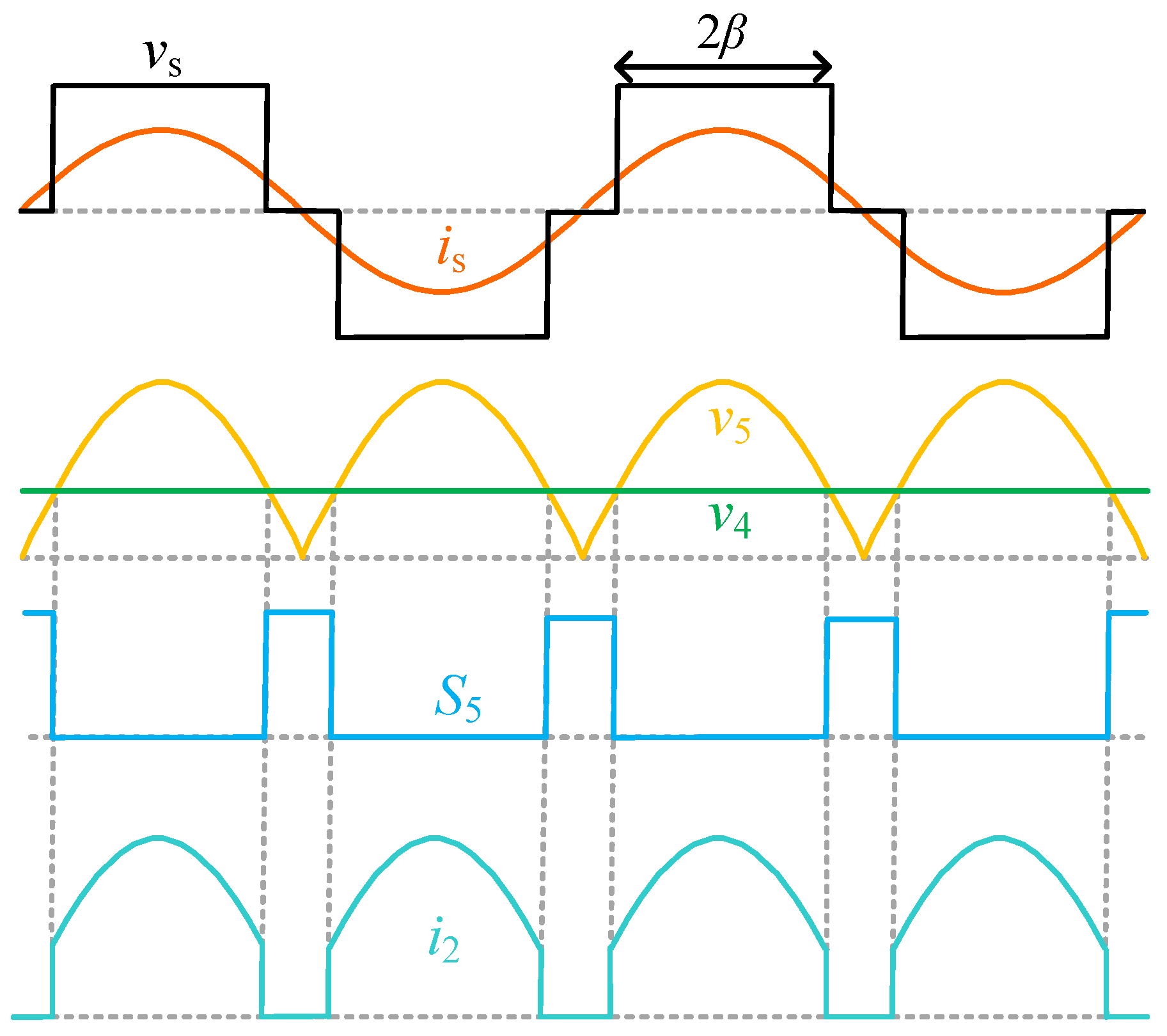
Figure 8 shows the typical waveforms of the APC receiver. When Io (or Uo) is greater than (or ), v1 is greater than Uref, and the comparator generates a zero v2. Otherwise, a positive v2 is produced. v3 decreases for a positive v2 and increases for a zero v2. Since v3 is negative, an inverting amplifier is used. The ratio of R8 versus R7 can regulate the response characteristic. is flows through R9, and the voltage drop is amplified by R10 and R11, which obtains a half-wave voltage v5. Then, v4 and v5 are sent to a comparator, and they can produce the desired control signal. After passing the non-isolated driver circuit, the gate drive signal is fed to the switch. When S5 is turned on, the receiver is short-circuited, which results in a zero vs. When S5 is turned off, vs becomes Uo or −Uo. β is automatically regulated by the feedback signals.
The CC and CV power transfer modes can be achieved through the proposed analog controller. Meanwhile, the receiver does not require synchronization techniques and additional programming. Thus, the proposed APC method significantly reduces the difficulty in implementation, the cost, volume, and weight of the receiver.
4. Simulation and Experiment
Results are obtained from simulation studies in PLECS and hardware prototype experiments. Both results are presented and compared to validate the feasibility of the proposed topology and control methods. The main parameters of the WPT system are listed in Table 1. Lp and Ls are 150 μH and 200 μH with a coil distance of 10 cm. The primary and secondary coils are compensated by 23 nF and 17 nF resonant capacitors, respectively. The inverting frequency of the transmitter is 85 kHz. The diodes are MUR3020PT, with a low forward voltage drop of 1 V. SiC MOSFETs are SCT3030KL. Heat sinks are installed on each diode and MOSFET.
4.1. Digital Phase Control
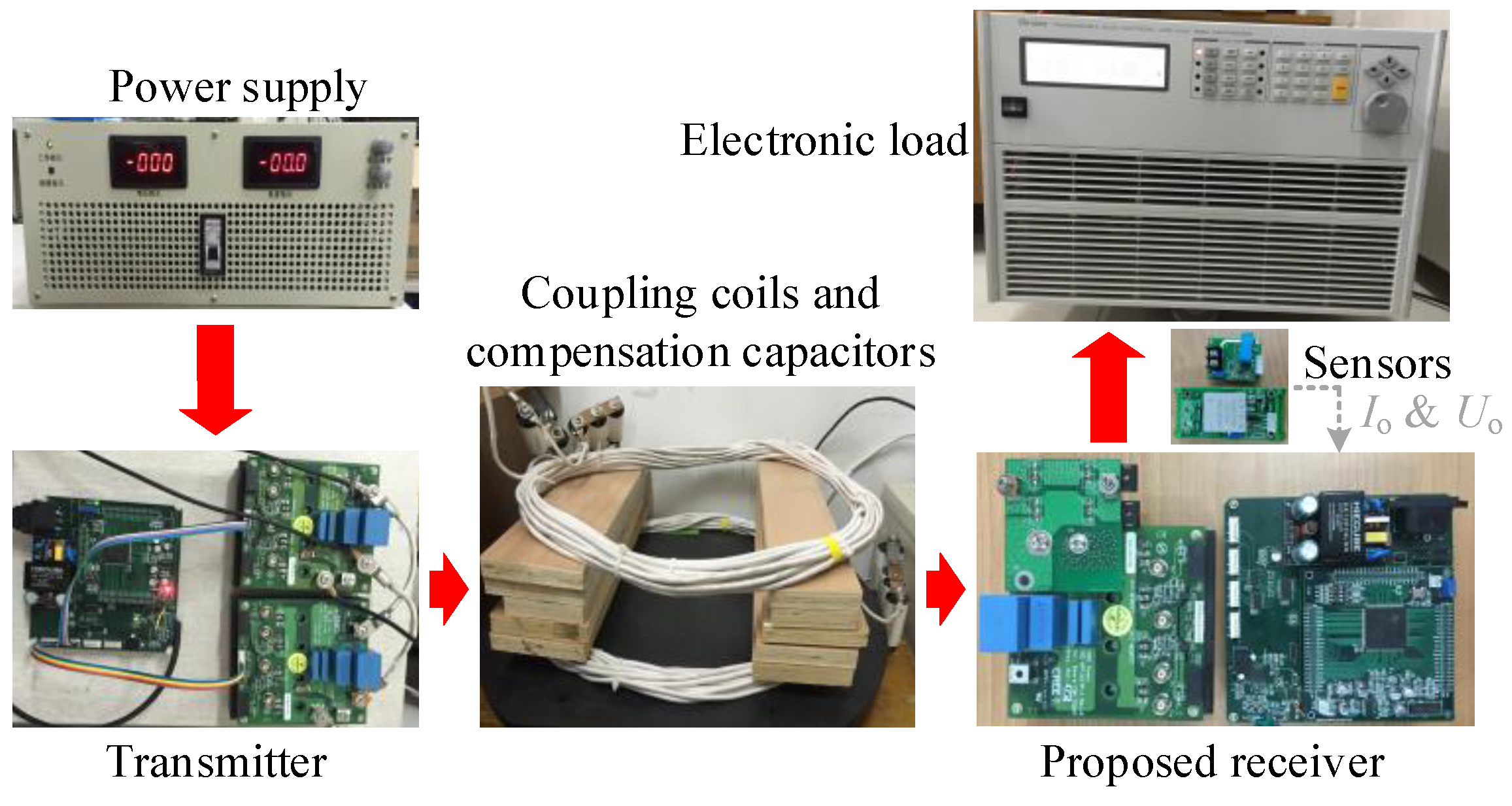
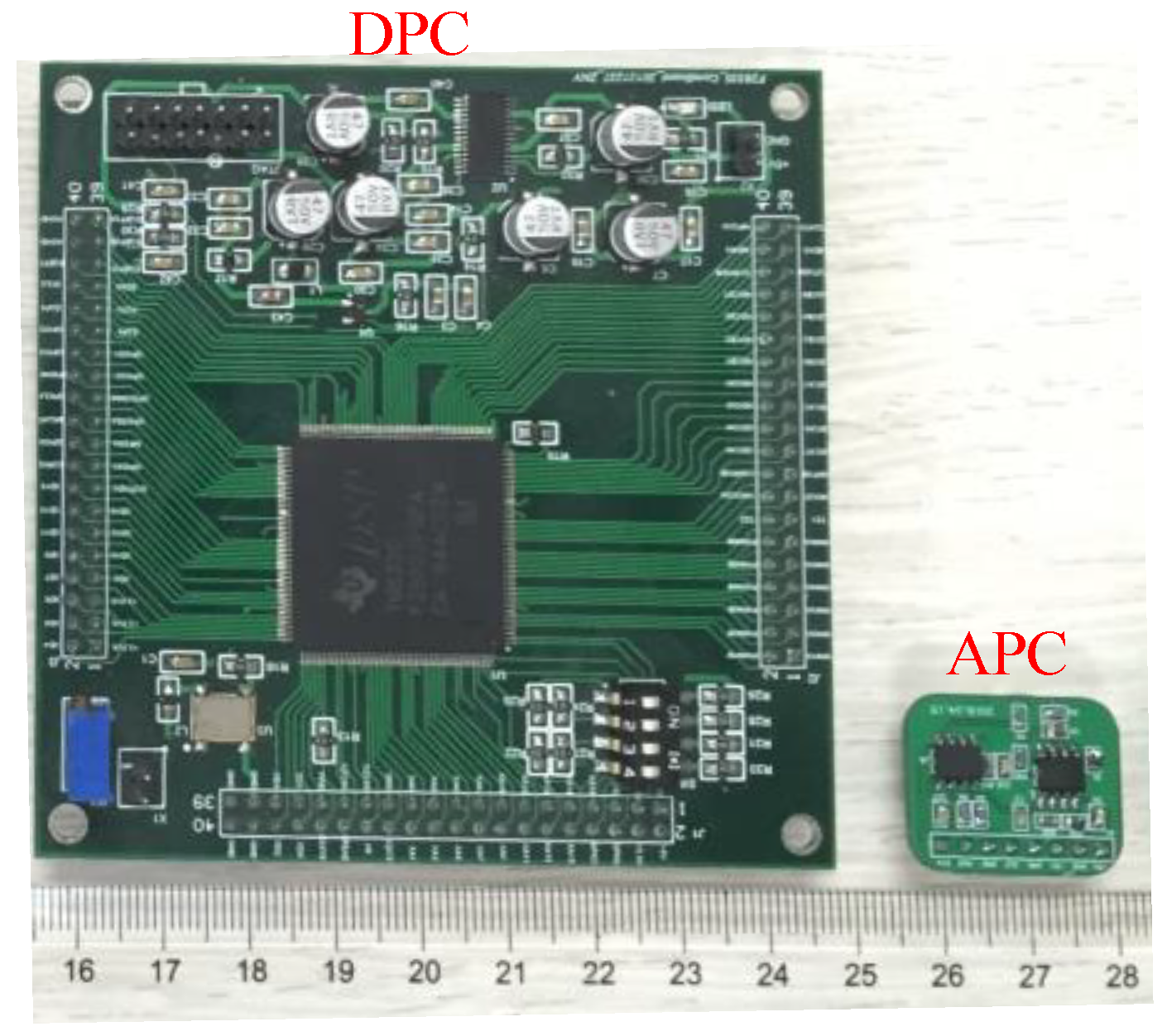
The prototype photograph of the DPC system is shown in Figure 9. Two TMS320F28335 chips are used as the primary and secondary controllers. The transmitter inverts the DC voltage into high frequency resonant voltage vp. Then, vs is induced by the magnetic field generated by ip. Afterwards, secondary resonant current is is rectified into DC current Io by the proposed receiver. Finally, the power is consumed by Chroma programmable AC-DC electronic load model 63803. Current and voltage sensors are installed to sample the feedback signals for power regulation. ACPL-W346 chips are used as the isolated drivers which are supplied by isolated DC-DC converter G1212S-2W.
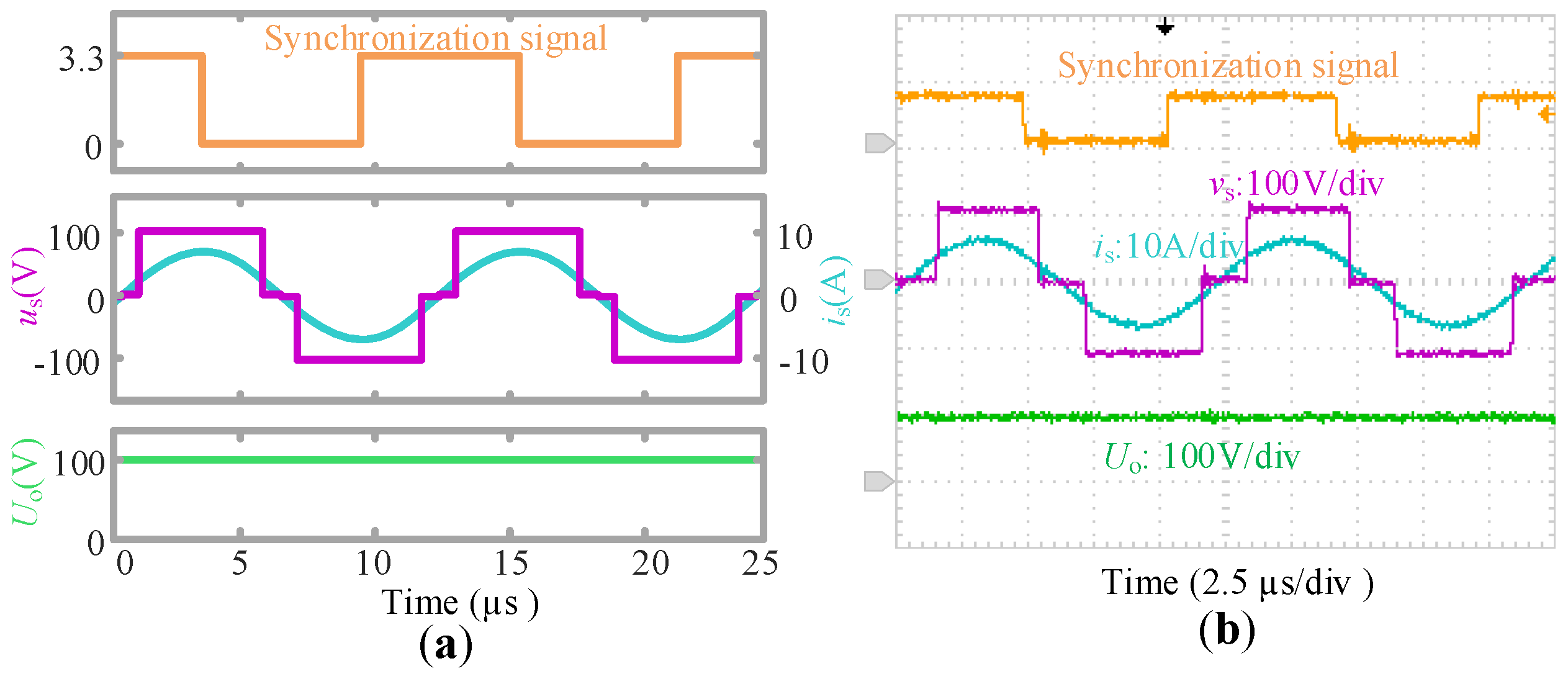
Figure 10 shows the typical waveforms of the DPC receiver. To ensure that the signal fed to the comparator stays within a proper range, the values of the divider resistances should be configured with the power level. In this paper, the high-side resistance Rh is 2 MΩ and the low-side resistance Rl is 10 kΩ. The voltage across Cp generates the synchronization signal, and it is fed to GPIO6 of the controller. vs and is are controlled to be in phase. The desired output voltage or current is realized by regulating β.
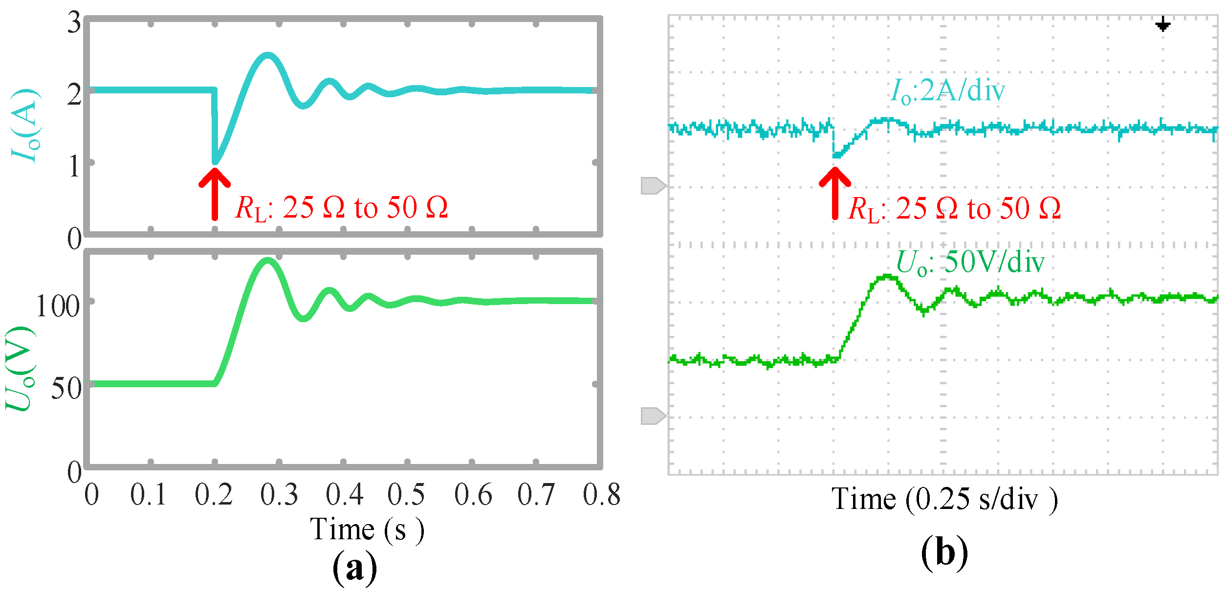
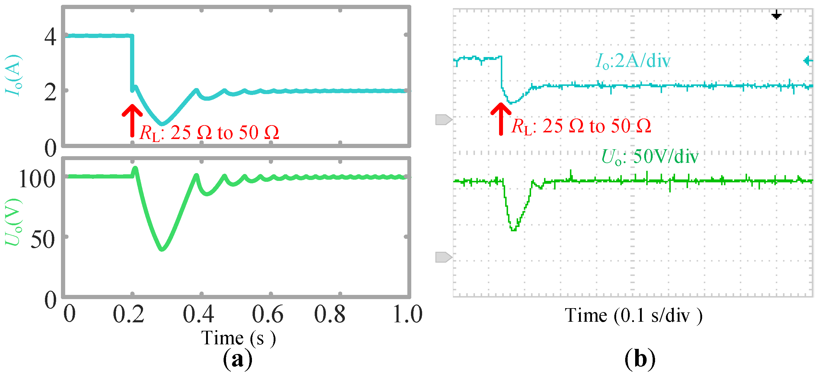
Figure 11a,b shows the simulated and experimental CC power transfer results by DPC. The reference current is set at 2 A, and RL changes from 25 Ω to 50 Ω. When RL is 25 Ω, the simulated and experimental values of β are 27.8° and 27.4°, respectively. The simulated and experimental output currents are 2.00 A and 1.96 A, which correspond to 83.3% and 80.8% DC-to-DC efficiencies, respectively. When RL is 50 Ω, the simulated and experimental values of β are 28.6° and 27.5°, respectively. The simulated and experimental output currents are 1.99 A and 1.97 A, with DC-to-DC efficiencies of 90.0% and 86.2%, respectively. Io keeps unchanged against load variations.
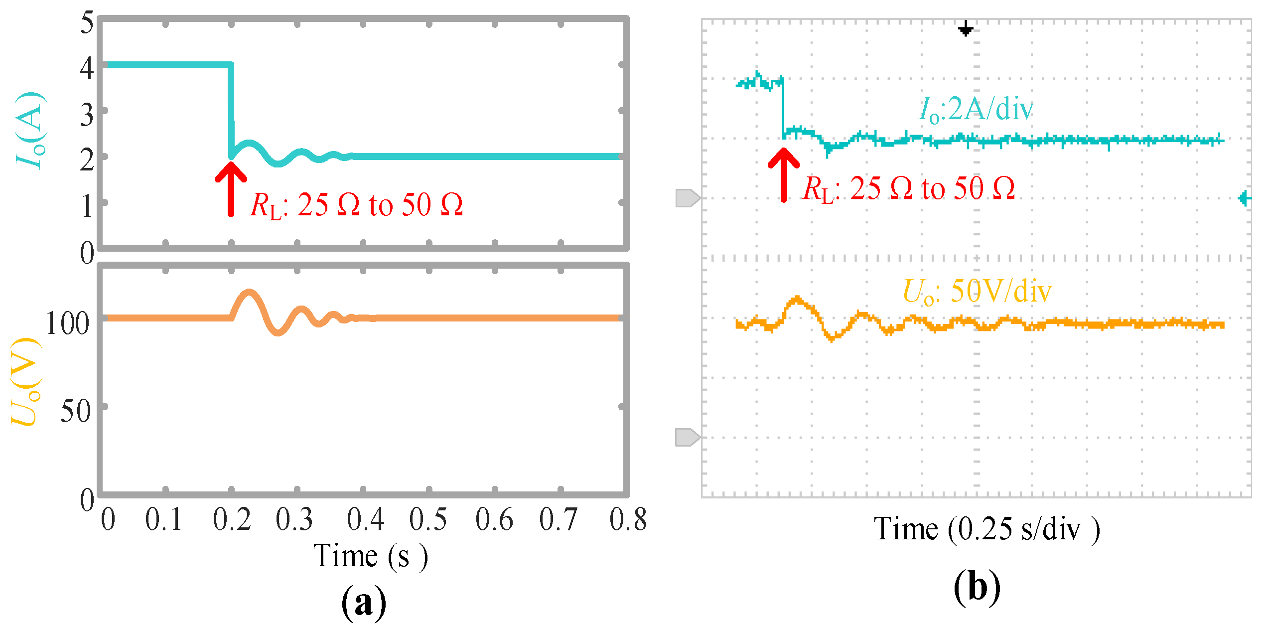
Figure 12a,b shows the simulated and experimental CV power transfer results by DPC. The reference voltage is set at 100 V. When RL is 25 Ω, the simulated and experimental values of β are 73.9° and 73.5°, which produce 100.0 V and 101.2 V output voltages, respectively. The simulated and experimental efficiencies are 93.1% and 91.4%, respectively. When RL is 50 Ω, the simulated and experimental values of β become 27.7° and 28.1°, respectively. The corresponding output voltages are 99.5 V and 100.5 V, with DC-to-DC efficiencies of 90.0% and 85.8%, respectively. During load variations, Uo remains at the desired level by regulating β accordingly.
4.2. Analog Phase Control
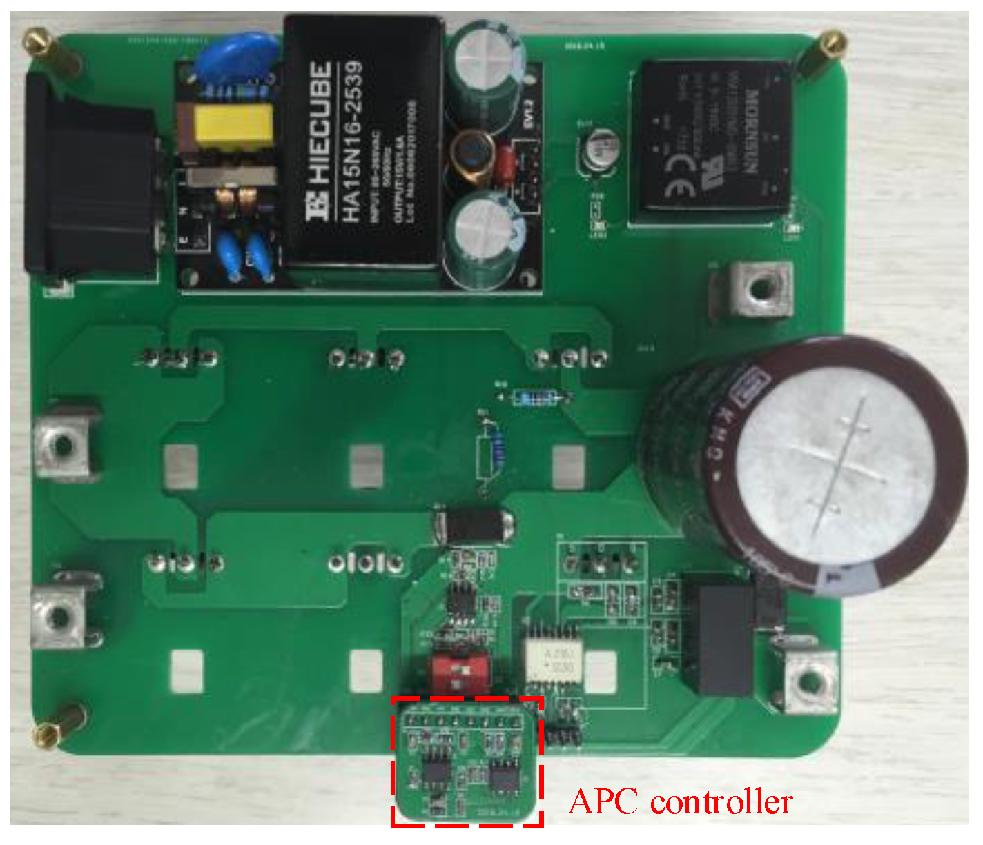
A photograph of the APC receiver is shown in Figure 13. Uref is set at 2.5 V. The divider resistances R1 and R2 are 91 kΩ and 2.2 kΩ, respectively. The sampling resistances R3 and R9 are 10 mΩ. R4 and R5 are 0.5 kΩ (1 kΩ//1 kΩ) and 62 kΩ, respectively. The ratios of R7 versus R8 and R11 versus R10 are 1 and 22, which ensures v4 and v5 falling within proper ranges. TLV3502 and THS4062 are used as the comparator and the operational amplifier, respectively. The configurations of the simulations are identical to the experimental prototype.
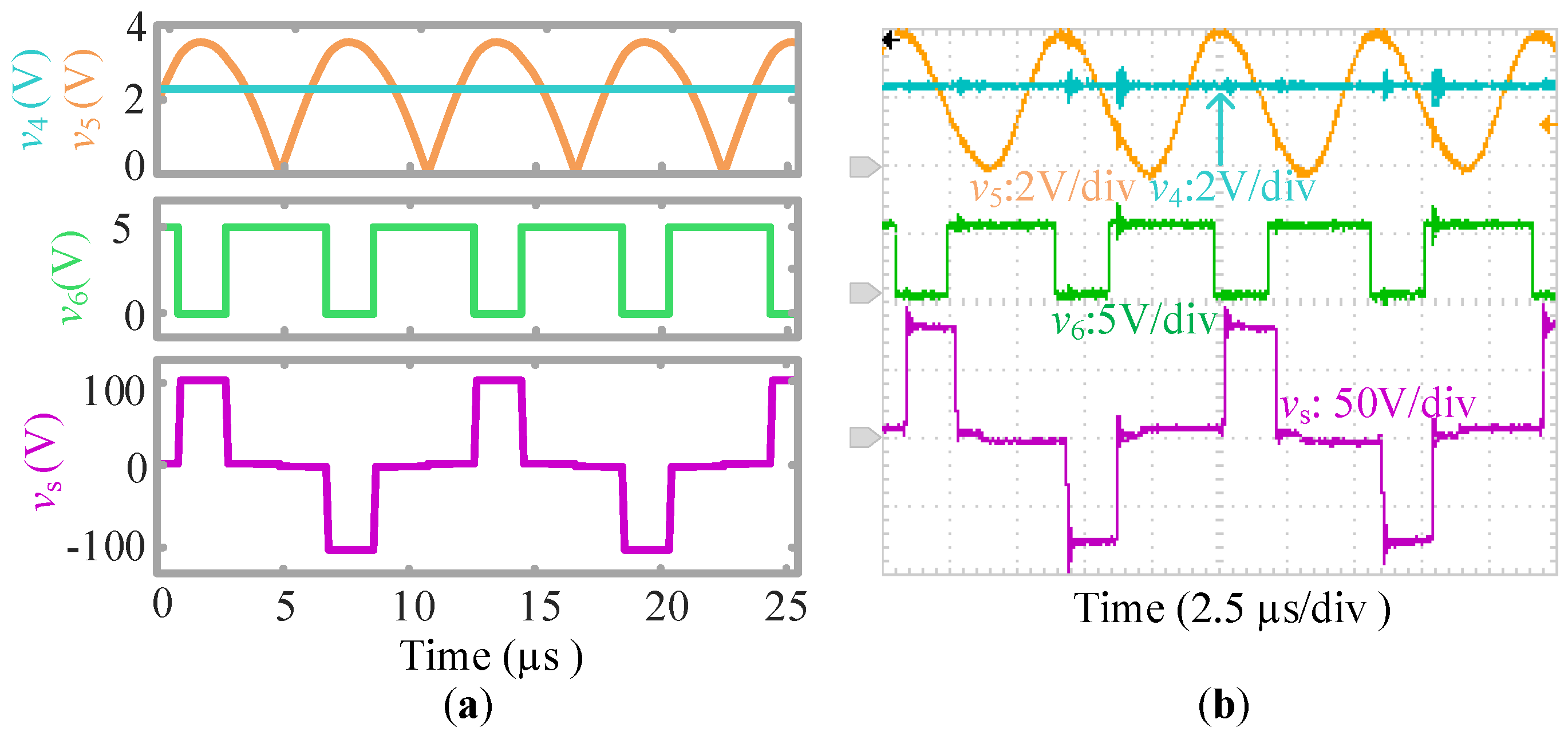
Figure 14 shows the logical waveforms of the APC receiver, including v4, v5, v6, and vs. Regulation circuits are installed on the main circuit. v4 and v5 are sent to TLV3502 which generates the control signal. When v5 is smaller than v4, v6 becomes high level, and S5 is turned on. Otherwise, v6 becomes low level, and S5 is turned off. Small oscillations appear in v6, which should be interferences caused by the switching processes. When Io or Uo is smaller than the expected value, v4 decreases which brings about a larger β. Otherwise, v4 increases, and a smaller β is produced.
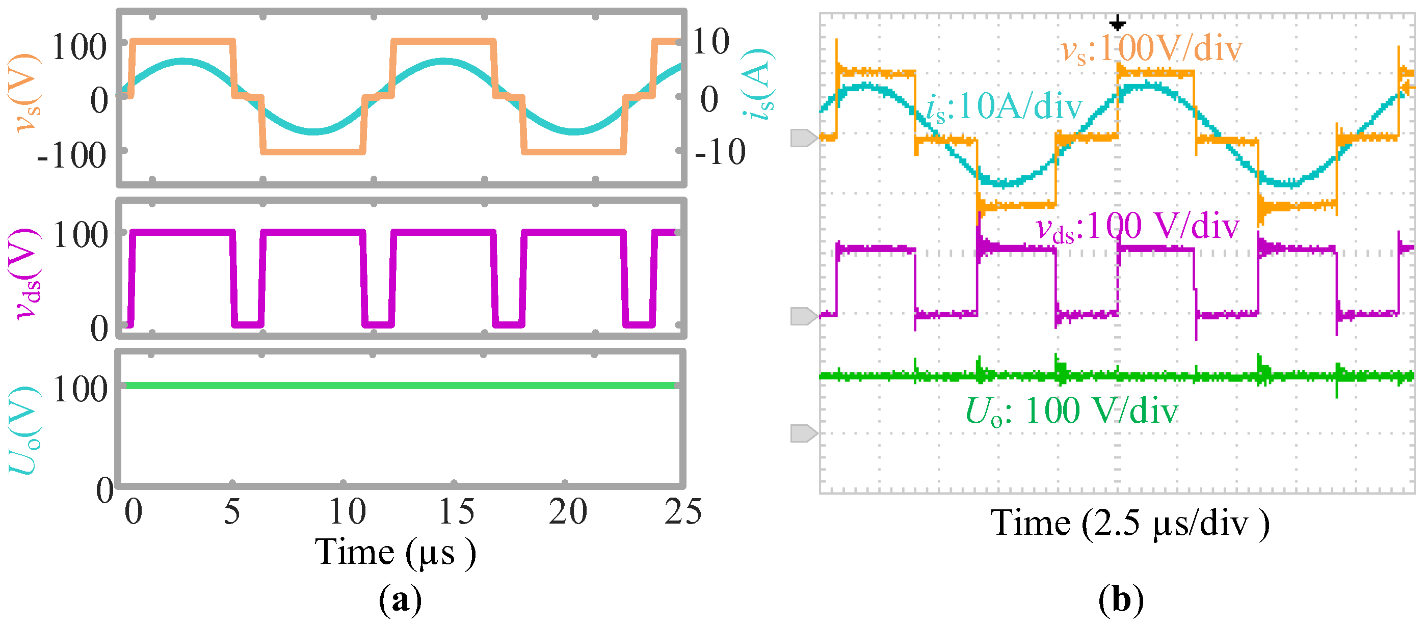
Figure 15 shows the typical waveforms of the APC receiver. In simulations, vs is in phase with is. However, in experiments, it takes some time for the signal to go through the operational amplifier, the comparator, the DSP, and the driver circuit. This time delay results in vs lagging is by some degrees. High performance devices can reduce this time delay.
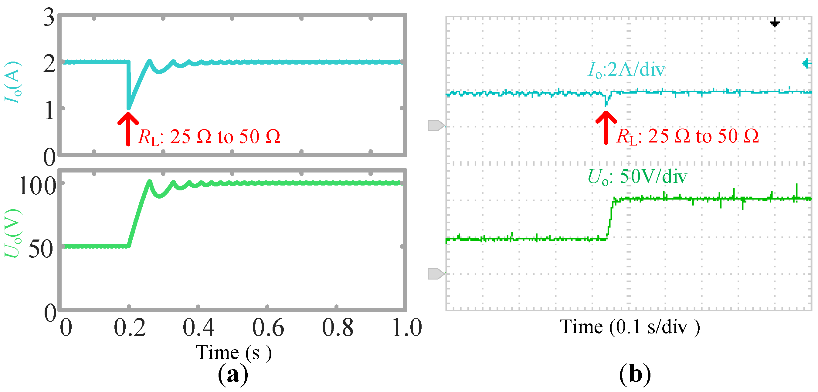
Figure 16a,b shows the simulated and experimental results of the CC power transfer by APC. When RL is 25 Ω, the simulated and experimental output currents are 1.99 A and 1.98 A, respectively. The simulated and experimental DC-to-DC efficiencies are 82.5% and 78.2%. When RL is 50 Ω, the simulated and experimental output currents are 1.99 A and 1.94 A, which correspond to 89.5% and 85.2% DC-to-DC efficiencies, respectively. In the CC mode, Io maintains at the desired 2 A against load variations.
Figure 17a,b shows the simulated and experimental results of the CV power transfer by APC. The reference voltage is set at 100 V. When RL is 25 Ω, the simulated and experimental output voltages are 99.7 V and 103.7 V, whose DC-to-DC efficiencies are 92.2% and 88.9%, respectively. When RL is 50 Ω, the simulated and experimental output voltages are 99.5 V and 104.6 V, respectively. The overall simulated and experimental efficiencies are 89.4% and 84.7%, respectively. In the CV mode, Uo remains unchanged against load variations.
Since simulations are closer to an ideal system than experiments, their efficiencies are higher than experimental ones. However, the dynamic and static performance are generally the same, which verifies the feasibility of the APC system.
4.3. Comparisons between Proposed Methods
Figure 18 shows the photograph of the two proposed controllers. The DPC controller is 9.0 cm × 9.0 cm × 2.7 cm, whereas the APC controller is only 2.4 cm × 2.0 cm × 0.3 cm. The analog controller is much smaller than the digital one. The volume, weight, and cost of the analog receiver can be significantly reduced.
Although both the DPC and APC methods can realize the CC and CV power transfer modes, they differ in some aspects. Table 2 compares the differences of the two proposed methods. The DPC system is more complex: it requires a DSP controller, isolated power supplies and driver circuits, current and voltage sensors, and the synchronization circuit. However, the DPC system can eliminate the time delay caused by the regulation circuit and avoid additional power losses of the sampling and divider resistances in the APC receiver. The highest measured experimental efficiency of the APC system is 89.4%, whereas it is 91.4% in the DPC system. Thus, the DPC receiver contributes to a higher performance compared to the APC receiver. Furthermore, it is easier to change the received power through the software code as in the DPC system than changing the regulation resistances as in the APC system, i.e., the DPC system has a greater flexibility than the APC system. Conversely, the APC receiver is simpler since it does not require synchronization algorithms and dedicated programming. In addition, it needs fewer auxiliary devices, i.e., isolated power supplies and expensive sensors are not needed, as well as has a smaller printed circuit board layout. This makes the analog receiver lighter, more cost-effective, and compact.
4.4. Comparisons among Different Topologies of WPT Receivers
Comparisons among different WPT receivers are presented in Table 3, and the advantages of the proposed topology and control methods are demonstrated below.
Compared to DC-DC converters used in the WPT systems, the proposed receiver advances in two aspects. Firstly, fewer capacitors and no inductors are required in the proposed receiver. It can reduce the volume and weight of the receiver. Secondly, AC-DC and DC-DC conversions are achieved simultaneously by the proposed receiver. Fewer cascaded circuits, therefore, bring about a higher overall efficiency.
Compared to full bridge and semi-bridgeless topologies, the proposed receiver advances in two aspects: Firstly, the proposed receiver is more cost-effective since the number of SiC MOSFETs and driver circuits used in the proposed receiver have been reduced by 75% as compared to full bridge topology, and 50% as compared to semi-bridgeless topology. In addition, a SiC diode, aiming to reduce high forward voltage, is not needed in the proposed receiver. Therefore, the cost reduction can be significant. Secondly, the proposed receiver has a higher reliability. Dead time is required to avoid short circuit in full bridge applications, whereas the proposed receiver gets rid of short circuit due to the reverse blocking of the diode.
Most reported single-switch receivers are half-controlled, which may fail to achieve the CC and CV power transfer modes. Furthermore, the receivers require a large capacitor to stabilize the output voltage due to the usage of duty ratio control. However, the proposed receiver is full-controlled and has a strong power regulation ability. Owing to the utilization of PC, a small filter capacitor is needed in the proposed receiver.
5. Conclusions
This paper presents a novel single-switch phase controlled active rectifier as receiver for WPT systems. Improved DPC and APC methods are proposed based on the receiver topology to achieve effective CC and CV power transfer modes. The proposed method prevents forward voltage losses in SiC switches and accidental shoot through states with improved switching patterns. The system is easy to implement, has a lower cost, smaller volume, lighter weight, and a higher reliability than conventional phase controlled receivers. Detailed analyses of the operating modes and implementation techniques are presented. Simulated and experimental results of a 400-W WPT system are included which show more than 91% overall efficiency and thereby demonstrate the feasibility of the proposed system.
Author Contributions
X.L., H.T., and X.Y. conceptualized the main idea of this research project; X.L. designed and conducted the experiments; N.J. and D.M. checked the results; X.L. wrote the whole paper; and N.J., D.M. and K.H. reviewed and edited the paper.
Funding
This research was funded by United Foundation of NSFC-Henan, grant number U1604136. The APC was funded by Houjun Tang.
Conflicts of Interest
The authors declare no conflict of interest.
References
- Villa, J.L.; Sallan, J.; Osorio, J.F.S.; Llombart, A. High-misalignment tolerant compensation topology for ICPT systems. IEEE Trans. Ind. Electron. 2012, 59, 945–951. [Google Scholar] [CrossRef]
- Ahn, D.; Hong, S. Wireless power transmission with self-regulated output voltage for biomedical implant. IEEE Trans. Ind. Electron. 2014, 61, 2225–2235. [Google Scholar] [CrossRef]
- Wu, H.H.; Gilchrist, A.; Sealy, K.D.; Bronson, D. A High Efficiency 5 kW Inductive Charger for EVs Using Dual Side Control. IEEE Trans. Ind. Inform. 2012, 8, 585–595. [Google Scholar] [CrossRef] [Green Version]
- Patil, D.; Sirico, M.; Lei, G.; Fahimi, B. Maximum Efficiency Tracking in Wireless Power Transfer for Battery Charger: Phase Shift and Frequency Control. In Proceedings of the 2016 IEEE Energy Conversion Congress and Exposition (ECCE), Milwaukee, WI, USA, 18–22 September 2016; Volume 99. [Google Scholar]
- Li, H.; Li, J.; Wang, K.; Chen, W.; Yang, X. A maximum efficiency point tracking control scheme for wireless power transfer systems using magnetic resonant coupling. IEEE Trans. Power Electron. 2015, 30, 3998–4008. [Google Scholar] [CrossRef]
- Zhong, W.X.; Hui, S.Y.R. Maximum energy efficiency tracking for wireless power transfer systems. IEEE Trans. Power Electron. 2015, 30, 4025–4034. [Google Scholar] [CrossRef]
- Fu, M.; Yin, H.; Zhu, X.; Ma, C. Analysis and tracking of optimal load in wireless power transfer systems. IEEE Trans. Power Electron. 2015, 30, 3952–3963. [Google Scholar] [CrossRef]
- Ahn, D.; Hong, S. Wireless power transfer resonance coupling amplification by load-modulation switching controller. IEEE Trans. Ind. Electron. 2015, 62, 898–909. [Google Scholar] [CrossRef]
- Yuan, L.; Li, B.; Zhang, Y.; He, F.; Chen, K.; Zhao, Z. Maximum efficiency point tracking of the wireless power transfer system for the battery charging in electric vehicles. In Proceedings of the 2015 18th International Conference on Electrical Machines and Systems (ICEMS), Pattaya, Thailand, 25–28 October 2015; pp. 1101–1107. [Google Scholar]
- Li, S.; Mi, C.C. Wireless Power Transfer for Electric Vehicle Applications. IEEE J. Emerg. Sel. Top. Power Electron. 2015, 3, 4–17. [Google Scholar]
- Dai, X.; Li, X.; Li, Y.; Hu, P. Maximum Efficiency Tracking for Wireless Power Transfer Systems with Dynamic Coupling Coefficient Estimation. IEEE Trans. Power Electron. 2018, 33, 5005–5015. [Google Scholar] [CrossRef]
- Bac, X.N.; Vilathgamuwa, D.M.; Foo, G.H.B.; Wang, P.; Ong, A.; Madawala, U.K.; Trong, D.N. An Efficiency Optimization Scheme for Bidirectional Inductive Power Transfer Systems. IEEE Trans. Power Electron. 2015, 30, 6310–6319. [Google Scholar]
- Thrimawithana, D.J.; Madawala, U.K.; Neath, M. A Synchronization Technique for Bidirectional IPT Systems. IEEE Trans. Ind. Electron. 2013, 60, 301–309. [Google Scholar] [CrossRef]
- Thrimawithana, D.J.; Madawala, U.K.; Yu, S. Design of a bi-directional inverter for a wireless V2G system. In Proceedings of the 2010 IEEE International Conference on Sustainable Energy Technologies (ICSET), Kandy, Sri Lanka, 6–9 September 2010; pp. 1–5. [Google Scholar]
- Madawala, U.K.; Neath, M.; Thrimawithana, D.J. A Power–Frequency Controller for Bidirectional Inductive Power Transfer Systems. IEEE Trans. Ind. Electron. 2013, 60, 310–317. [Google Scholar] [CrossRef]
- Madawala, U.K.; Thrimawithana, D.J. A Bidirectional Inductive Power Interface for Electric Vehicles in V2G Systems. IEEE Trans. Ind. Electron. 2011, 58, 4789–4796. [Google Scholar] [CrossRef]
- Neath, M.J.; Swain, A.K.; Madawala, U.K.; Thrimawithana, D.J. An optimal PID controller for a bidirectional inductive power transfer system using multiobjective genetic algorithm. IEEE Trans. Power Electron. 2014, 29, 1523–1531. [Google Scholar] [CrossRef]
- Tang, Y.; Chen, Y.; Madawala, U.K.; Thrimawithana, D.J.; Ma, H. A New Controller for Bi-directional Wireless Power Transfer Systems. IEEE Trans. Power Electron. 2018, 33, 9067–9087. [Google Scholar] [CrossRef]
- Zhao, L.; Thrimawithana, D.; Madawala, U. A Hybrid Bi-directional Wireless EV Charging System Tolerant to Pad Misalignment. IEEE Trans. Ind. Electron. 2018, 64, 7079–7086. [Google Scholar] [CrossRef]
- Mai, R.; Ma, L.; Liu, Y.; Yue, P.; Cao, G.; He, Z. A Maximum Efficiency Point Tracking Control Scheme Based on Different Cross Coupling of Dual-Receiver Inductive Power Transfer System. Energies 2017, 10, 217. [Google Scholar] [CrossRef]
- Diekhans, T.; De Doncker, R.W. A dual-side controlled inductive power transfer system optimized for large coupling factor variations and partial load. IEEE Trans. Power Electron. 2015, 30, 6320–6328. [Google Scholar] [CrossRef]
- Berger, A.; Agostinelli, M.; Vesti, S.; Oliver, J.A.; Cobos, J.A.; Huemer, M. A Wireless Charging System Applying phase-Shift and Amplitude Control to Maximize Efficiency and Extractable Power. IEEE Trans. Power Electron. 2015, 30, 6338–6348. [Google Scholar] [CrossRef]
- Mai, R.; Liu, Y.; Li, Y.; Yue, P.; Cao, G.; He, Z. An Active Rectifier Based Maximum Efficiency Tracking Method Using an Additional Measurement Coil for Wireless Power Transfer. IEEE Trans. Power Electron. 2017, 33, 716–728. [Google Scholar] [CrossRef]
- Liu, X.; Wang, T.; Yang, X.; Jin, N.; Tang, H. Analysis and Design of a Wireless Power Transfer System with Dual Active Bridges. Energies 2017, 10, 1588. [Google Scholar] [CrossRef]
- Liu, X.; Wang, T.; Yang, X.; Tang, H. Analysis of Efficiency Improvement in Wireless Power Transfer System. IET Power Electron. 2018, 11, 302–309. [Google Scholar] [CrossRef]
- Colak, K.; Asa, E.; Bojarski, M.; Czarkowski, D.; Onar, O.C. A Novel Phase-Shift Control of Semibridgeless Active Rectifier for Wireless Power Transfer. IEEE Trans. Power Electron. 2015, 30, 6288–6297. [Google Scholar] [CrossRef]
- Mai, R.K.; Liu, Y.; Chen, Y. Studies of Efficiency Optimization Methods Based on Optimal Equivalent Load Control in IPT Systems. Proce. CSEE 2016, 36, 6468–6475. [Google Scholar]
- Ahn, D.; Kim, S.; Moon, J.; Cho, I.K. Wireless Power Transfer with Automatic Feedback Control of Load Resistance Transformation. IEEE Trans. Power Electron. 2016, 31, 7876–7886. [Google Scholar] [CrossRef]
- Tian, J.; Hu, A.P.; Nguang, S.K. Secondary Side Output Voltage Stabilization of an IPT System by Tuning/Detuning through a Serial Tuned DC Voltage-controlled Variable Capacitor. J. Power Electron. 2017, 17, 570–578. [Google Scholar] [CrossRef] [Green Version]
- Abdolkhani, A. Single-switch soft-switched power flow controller for wireless power transfer applications. In Proceedings of the 2017 IEEE Wireless Power Transfer Conference (WPTC), Taipei, Taiwan, 10–12 May 2017; pp. 1–4. [Google Scholar]
- Kuroda, K.; Omori, H.; Kimura, N.; Morizane, T.; Fukuda, K.; Michikoshi, H. A wireless V2H apparatus with a new SiC-MOSFET and unique bidirectional controlled single-ended converter. In Proceedings of the 2017 IEEE 3rd International Future Energy Electronics Conference and ECCE Asia (IFEEC 2017 ECCE Asia), Kaohsiung, Taiwan, 3–7 June 2017; pp. 298–303. [Google Scholar]
- Murakami, A.; Omori, H.; Ohara, S.; Fukuda, K.; Michikoshi, H.; Kimura, N. Loss/resistance evaluation of SiC-MOSFET and Si-IGBT in a novel type of single-ended wireless V2H. In Proceedings of the 2017 IEEE PELS Workshop on Emerging Technologies: Wireless Power Transfer (WoW), Chongqing, China, 20–22 May 2017; pp. 1–6. [Google Scholar]
- Wang, T.; Liu, X.; Jin, N.; Tang, H.; Yang, X.; Ali, M. Wireless Power Transfer for Battery Powering System. Electronics 2018, 7, 178. [Google Scholar] [CrossRef]
- Boys, J.T.; Covic, G.A.; Xu, Y. DC analysis technique for inductive power transfer pick-ups. IEEE Power Electron. Lett. 2003, 99, 51–53. [Google Scholar] [CrossRef]
- Green, A.W.; Boys, J.T. 10 kHz inductively coupled power transfer-concept and control. In Proceedings of the 5th 1994 Fifth International Conference on Power Electronics and Variable-Speed Drives, London, UK, 26–28 October 1994; pp. 694–699. [Google Scholar]
- Boys, J.T.; Covic, G.A.; Green, A.W. Stability and control of inductively coupled power transfer systems. IEEE Proc. Electr. Power Appl. 2000, 147, 37–43. [Google Scholar] [CrossRef]
Figure 1.
WPT system with proposed single-switch receiver.

Figure 2.
Typical waveforms of proposed receiver. S5, gate drive signal (blue line); i1, current flowing through MOSFET (yellow line); i2, current flowing through D5 (light green line); is, secondary resonant current (orange line); vs, secondary resonant voltage (black line).
Figure 2.
Typical waveforms of proposed receiver. S5, gate drive signal (blue line); i1, current flowing through MOSFET (yellow line); i2, current flowing through D5 (light green line); is, secondary resonant current (orange line); vs, secondary resonant voltage (black line).

Figure 3.
Operating modes of proposed receiver: (a) Mode 1; (b) Mode 2; (c) Mode 3; (d) Mode 4; (e) Mode 5; and (f) Mode 6.
Figure 3.
Operating modes of proposed receiver: (a) Mode 1; (b) Mode 2; (c) Mode 3; (d) Mode 4; (e) Mode 5; and (f) Mode 6.

Figure 4.
Schematic of DPC system.

Figure 5.
Typical synchronization waveforms.

Figure 6.
Algorithm flowchart of DPC receiver.

Figure 7.
Schematic of APC system.

Figure 8.
Typical waveforms of APC receiver. is, secondary resonant current (orange line); vs, secondary resonant voltage (black line); v4, feedback signal (green line); v5, half-wave signal (yellow line); S5, gate drive signal (blue line); i2, current flowing through D5 (light green line).
Figure 8.
Typical waveforms of APC receiver. is, secondary resonant current (orange line); vs, secondary resonant voltage (black line); v4, feedback signal (green line); v5, half-wave signal (yellow line); S5, gate drive signal (blue line); i2, current flowing through D5 (light green line).

Figure 9.
Prototype photograph of DPC system.

Figure 10.
Typical waveforms of DPC receiver: (a) simulated; and (b) experimental. Synchronization signal (yellow lines); is, secondary resonant current (blue lines); vs, secondary resonant voltage (purple lines); Uo, output voltage (green lines).
Figure 10.
Typical waveforms of DPC receiver: (a) simulated; and (b) experimental. Synchronization signal (yellow lines); is, secondary resonant current (blue lines); vs, secondary resonant voltage (purple lines); Uo, output voltage (green lines).

Figure 11.
Simulated and experimental CC power transfer results of DPC system: (a) simulated; and (b) experimental. Io, output current (blue lines); Uo, output voltage (green lines).
Figure 11.
Simulated and experimental CC power transfer results of DPC system: (a) simulated; and (b) experimental. Io, output current (blue lines); Uo, output voltage (green lines).

Figure 12.
Simulated and experimental CV power transfer results of DPC system: (a) simulated; and (b) experimental. Io, output current (blue lines); Uo, output voltage (yellow lines).
Figure 12.
Simulated and experimental CV power transfer results of DPC system: (a) simulated; and (b) experimental. Io, output current (blue lines); Uo, output voltage (yellow lines).

Figure 13.
Photograph of APC receiver.

Figure 14.
Logical waveforms of APC receiver: (a) simulated; and (b) experimental. v4, feedback signal (blue lines); v5, half-wave signal (yellow lines); v6, control signal (green lines); vs, secondary resonant voltage (purple lines).
Figure 14.
Logical waveforms of APC receiver: (a) simulated; and (b) experimental. v4, feedback signal (blue lines); v5, half-wave signal (yellow lines); v6, control signal (green lines); vs, secondary resonant voltage (purple lines).

Figure 15.
Typical waveforms of APC receiver: (a) simulated; and (b) experimental. Is: secondary resonant current (blue lines); vs, secondary resonant voltage (yellow lines); vds, voltage across S5 (purple lines); Uo, output voltage (green lines).
Figure 15.
Typical waveforms of APC receiver: (a) simulated; and (b) experimental. Is: secondary resonant current (blue lines); vs, secondary resonant voltage (yellow lines); vds, voltage across S5 (purple lines); Uo, output voltage (green lines).

Figure 16.
Simulated and experimental CC power transfer results of APC system: (a) simulated; and (b) experimental. Io, output current (blue lines); Uo, output voltage (green lines).
Figure 16.
Simulated and experimental CC power transfer results of APC system: (a) simulated; and (b) experimental. Io, output current (blue lines); Uo, output voltage (green lines).

Figure 17.
Simulated and experimental CV power transfer results of APC system: (a) simulated; and (b) experimental. Io, output current (blue lines); Uo, output voltage (green lines).
Figure 17.
Simulated and experimental CV power transfer results of APC system: (a) simulated; and (b) experimental. Io, output current (blue lines); Uo, output voltage (green lines).

Figure 18.
Photograph of two proposed controllers.


Table 1.
Main parameters of WPT system.
| Symbol | Quantity | Value |
|---|---|---|
| Lp | coil inductance of transmitter | 150 μH |
| Ls | coil inductance of receiver | 200 μH |
| Cp | primary compensation capacitance | 23 nF |
| Cs | secondary compensation capacitance | 17 nF |
| f | inverting frequency | 85 kHz |
Table 2.
Comparisons between DPC and APC.
| Methods | DPC | APC |
|---|---|---|
| Complexity | High | Low |
| Performance | Very High | Good |
| Flexibility | Very High | Good |
| Cost | High | Low |
| Weight | Heavy | Light |
| Volume | Large | Small |
Table 3.
Comparisons among different receivers for WPT systems.
| Topologies | Capacitors | Inductors | Digital Controllers | Switches | Control Methods | Power Regulation Ability |
|---|---|---|---|---|---|---|
| DC-DC converters [3,4,5,6,7,8] | 2 | 1 | 1 | 1 | Duty ratio control | Full-controlled |
| Full bridge [12,13,14,15,16,17,18,19,20,21,22,23,24,25] | 1 | 0 | 1 | 4 | Phase control | Full-controlled |
| Semi-bridgeless [26,27] | 1 | 0 | 1 | 2 | Phase control | Full-controlled |
| Reported single-switch receivers [29,30,31,32,33] | 1 | 0 | 1 | 1 | Duty ratio control | Half-controlled |
| Proposed receiver | 1 | 0 | 0 or 1 | 1 | Phase control | Full-controlled |
© 2018 by the authors. Licensee MDPI, Basel, Switzerland. This article is an open access article distributed under the terms and conditions of the Creative Commons Attribution (CC BY) license (http://creativecommons.org/licenses/by/4.0/).
Share and Cite
MDPI and ACS Style
Liu, X.; Jin, N.; Yang, X.; Hashmi, K.; Ma, D.; Tang, H. A Novel Single-switch Phase Controlled Wireless Power Transfer System. Electronics 2018, 7, 281. https://doi.org/10.3390/electronics7110281
AMA Style
Liu X, Jin N, Yang X, Hashmi K, Ma D, Tang H. A Novel Single-switch Phase Controlled Wireless Power Transfer System. Electronics. 2018; 7(11):281. https://doi.org/10.3390/electronics7110281
Chicago/Turabian StyleLiu, Xin, Nan Jin, Xijun Yang, Khurram Hashmi, Dianguan Ma, and Houjun Tang. 2018. "A Novel Single-switch Phase Controlled Wireless Power Transfer System" Electronics 7, no. 11: 281. https://doi.org/10.3390/electronics7110281
Note that from the first issue of 2016, this journal uses article numbers instead of page numbers. See further details here.