Article

A Software Framework for Rapid Application-Specific Hybrid Photonic Network-on-Chip Synthesis †

1
Micron Technology, Non-Volatile Engineering, Longmont, CO 80501, USA
2
Department of Electrical and Computer Engineering, Colorado State University, Fort Collins, CO 80523, USA
*
Author to whom correspondence should be addressed.
This paper is an extended version of our paper published in the proceedings of the IEEE International Symposium on Quality Electronic Design 2012 conference as S. Bahirat, S. Pasricha, “A Particle Swarm Optimization Approach for Synthesizing Application-specific Hybrid Photonic Networks-on-Chip”, IEEE International Symposium on Quality Electronic Design (ISQED), pp. 78-83, March. 2012.
Electronics 2016, 5(2), 21; https://doi.org/10.3390/electronics5020021
Submission received: 6 April 2016 / Revised: 27 April 2016 / Accepted: 29 April 2016 / Published: 14 May 2016

Abstract

:
Network on Chip (NoC) architectures have emerged in recent years as scalable communication fabrics to enable high bandwidth data transfers in chip multiprocessors (CMPs). These interconnection architectures still need to conquer many challenges, e.g., significant power consumption and high data transfer latencies. Hybrid electro-photonic NoCs have been recently proposed as a solution to mitigate some of these challenges. However, with increasing application complexity, hardware dependencies, and performance variability, optimization of hybrid photonic NoCs requires traversing a massive design space. To date, prior work on software tools for rapid automated NoC synthesis have mainly focused on electrical NoCs. In this article, we propose a novel suite of software tools for effectively synthesizing hybrid photonic NoCs. We formulate and solve the synthesis problem using four search-based optimization heuristics: (1) Ant Colony Optimization (ACO); (2) Particle Swarm Optimization (PSO); (3) Genetic Algorithm (GA); and (4) Simulated Annealing (SA). Our experimental results show significant promise for the ACO and PSO based heuristics. Our novel implementation of PSO achieves an average of 64% energy-delay product improvements over GA and 53% improvement over SA; while our novel ACO implementation achieves 107% energy-delay product improvements over GA and 62% improvement over SA.

Graphical Abstract

1. Introduction

According to the ITRS roadmap [1], Complementary metal–oxide–semiconductor (CMOS) feature sizes will shrink to sub-10 nm regime within the next five years. It is also projected that by 2020, as many as 256 cores would be integrated onto a single die. With the advent of such highly parallel chip multiprocessors (CMPs), the design of the network-on-chip (NoC) interconnection fabric [2] will be crucial to ensure that compute cores are able to communicate with L2-L4 cache banks, main memory modules, and other I/O devices with high bandwidths, low latencies, and minimal power dissipation. However, electrical NoCs today are already severely constrained due to their long multi-hop latencies and high power dissipation, which will make it practically impossible to stay within the limited on-chip power budget while meeting performance constraints in the near future. CMOS compatible on-chip photonic interconnects with silicon-on-insulator (SOI) waveguides provide a potential substitute for on-chip electrical interconnects, particularly for global on-chip communication, allowing data to be transferred across a chip with much faster light signals [3]. Based on recent technological advancements, the critical length at which photonic interconnects are advantageous over electrical interconnects has fallen to well below chip die dimensions [4].
To minimize on-chip communication power dissipation, research in recent years, e.g., [4,5,6,7,8,9,10,11,12,13], has focused on novel hybrid photonic NoC architectures that optimize the distribution of local and global communication between electrical and photonic links. The optimization of these hybrid photonic NoCs for parallel embedded applications requires traversing a massive design space to determine suitable application-specific values for hybrid photonic NoC parameters such as wavelength division multiplexing (WDM) density, number of photonic uplinks, serialization degree, etc. (these parameters are discussed in more detail in later sections) to maximize communication performance-per-watt. For example, a photonic NoC with n = 256 waveguides and up to m = 256 wavelengths per waveguide will require exploring n + (n)2 + (n)3 + ,…, + (n)m configurations (i.e., combinations of waveguides and wavelengths per waveguide) to find the most power efficient solution that also meets the performance goals for a given set of applications. This design space is practically exorbitant to traverse exhaustively. Moreover, these two parameters (waveguides, wavelengths) are just a small subset of the much larger set of parameters that must be explored during hybrid photonic NoC synthesis. Finding the best solution for such a combinatorial optimization problem that is known to be NP-hard could take years if we search through the entire solution space, even with leading-edge supercomputing technology today. Indeed, rapid application-driven optimization of hybrid photonic NoCs will become increasingly important as on-chip core counts increase, but this problem has not yet been addressed in prior work by researchers.
The only viable way to effectively solve the synthesis problem for hybrid photonic NoCs is by developing polynomial-time heuristics that permit us to identify and search through a relevant portion of the solution space in a tractable amount of time to find a near optimal solution. Greedy heuristics are unlikely to find good quality solutions due to their inclination for getting stuck in local optima. In contrast, non-greedy search heuristics such as Simulated Annealing (SA) [14] operate through repeated transformations and have the hill-climbing ability to escape local optima by allowing acceptance of worse solutions within the evaluation process. A population of solutions being simultaneously manipulated is one of the major differences between the SA and traditional greedy search algorithms. Approaches based on SA and other non-greedy iterative algorithms have proven highly effective in recent years for several difficult problems in the realm of VLSI physical design, such as partitioning and placement [15].
In this article, we address the problem of synthesizing (i.e., optimizing) application-specific hybrid photonic NoCs for emerging CMPs by adapting four diverse classes of search heuristics to our problem: (1) Particle Swarm Optimization (PSO) [16]; (2) Ant Colony Optimization (ACO) [17]; (3) Genetic Algorithm (GA) [18] and (4) Simulated Annealing (SA) [14]. Our experimental results demonstrate significant promise for these search heuristics, towards generating low power NoC communication fabrics that meet performance objectives.
This article is a significantly extended version of our previously published paper from ISQED 2012 [19] with the following major additions across the manuscript: (i) more comprehensive related work in Section 2 explaining how our contribution is different and novel in comparison with previously published architectures and software tools; (ii) more details on parameterized PRI, the serialization architecture, routing algorithm, and flow control for the hybrid photonic NoC architecture in Section 3; (iii) two new synthesis techniques based on ACO and GA algorithms, and a new core-to-tile mapping procedure in Section 5; and (iv) updated experimental results on new benchmarks and new synthesis algorithms in Section 6.

2. Related Work

2.1. Hybrid Photonic NoC Architectures

The idea of using photonics for communication on a chip was first introduced by Goodman et al. [3]. With advances in the fabrication and integration of photonic elements on a CMOS chip in recent years, several works have presented a comparison of the physical and circuit-level properties of on-chip electrical and photonic interconnects (e.g., [20,21,22]).
Several researchers have used silicon photonic device-level fabrication results as building blocks to propose hybrid photonic NoC architectures for emerging CMPs. For example, Le Beux et al. [5] proposed a hybrid photonic NoC with a point-to-point crossbar topology and electrical control network that uses on-chip lasers and allows the bandwidth between IP cores to be adapted according to application communication requirements. Vantrease et al. [7] proposed the Corona fully photonic crossbar with electrical buffering in the electrical realm. Corona utilizes an all-optical crossbar topology with photonic waveguides configured as token-based Multiple-Writer Single-Reader (MWSR) resource reservation systems. This architecture has higher photonic-layer complexity as it requires more than a million micro-ring resonators to implement all-optical crossbar. Corona also lacks communication path diversity, and makes use of expensive electro-photonic and photo-electronic conversions even for local transfers, which reduces its efficiency. Pan et al. [8] proposed the Firefly hierarchical photonic crossbar coupled with a concentrated mesh based electrical NoC. The architecture utilizes a hierarchical hybrid crossbar topology with clusters of nodes connected through local electrical networks, and nano-photonic links overlaid for global, inter-cluster communication. The photonic waveguides in the Firefly architecture are organized in a Reservation-assisted Single-Writer Multiple-Reader (R-SWMR) configuration. Even though this architecture comes somewhat close to our goal of creating a hybrid network that balances traffic among the electrical and photonic networks, still it has higher hardware overhead and lacks a methodology for controlling the distribution of traffic through the electrical and photonic paths. Shacham et al. [9] proposed a circuit-switched on-chip photonic torus network with reconfigurable broadband optical switches coupled with a topologically identical torus electrical NoC. Bahirat et al. [10] proposed concentric photonic rings coupled with a reconfigurable electrical mesh NoC. Li et al. [11] proposed a photonic broadcast bus with an electrical packet switched network. Joshi et al. [12] proposed a similar fully photonic NoC topology but using a Clos network and electrical buffering. The all-optical network based Clos topology is less complex than a full crossbar topology, however it still requires complex point-to-point photonic links and high-radix photonic routers. The Clos topology uses photonic interconnects even for transfers over short distances, which wastes power and leads to higher transfer latencies. Morris et al. [13] created a hybrid of an all-photonic crossbar and a photonic fat-tree.
Le Beux et al. [6] presented a very interesting comparative study of the worst-case optical losses of various crossbar based photonic NoCs, based on network topology, physical layout and waveguide insertion losses. Bahirat et al. [23] proposed a system-level CAD framework called HELIX for synthesizing application-specific hybrid nanophotonic-electric NoCs with an irregular topology, to optimize an architecture that combines free-space photonics with an electrical mesh NoC. Wang et al. [24] presented a software-defined photonic network-on-chip (SD-PNoC) based on a central controller to provide a global network topology that generates optimized routing paths. However this design suffers from scalability issues with long wires and has poor performance for heavy traffic loads. LumiNOC [25] reduces optical loss in photonic NoCs by partitioning the global network into multiple smaller sub-networks and using an arbitration scheme that utilizes the same wavelengths for channel arbitration and parallel data transmission. Ahmed et al. [26] proposed a hybrid silicon-photonic NoC architecture called PHENIC-II based on a light-weight electronic router and an energy efficient non-blocking optical switch. Pintus et al. [27] presented a theoretical framework to compare the NoCs with bus and ring topologies and concluded that ring NoCs can be more efficient compared to bus based topologies. Li et al. [28] proposed a cross-layer architecture to address the effect of temperature variations on photonic NoCs by varying the bias current through ring resonators and rerouting messages away from high temperature regions towards cooler regions to their destinations.
Out of all the existing photonic NoC architectures, we select the hybrid photonic ring/electrical mesh based topology from [10] as the baseline fabric for our synthesis effort due to its favorable low power and latency characteristics, coupled with its low implementation overhead. However, our synthesis approach can also be adapted to the other photonic NoC architectures discussed above.

2.2. NoC Synthesis Approaches

Significant research efforts have been focused on the study of mapping, routing and synthesis problems for regular as well as irregular NoC architectures. Efforts on regular NoC topology synthesis primarily focus on mapping uniform sized cores and their communication flows on regular mesh topologies to optimize energy and performance [29,30,31,32,33,34]. For instance, Ascia et al. [30] use a genetic algorithm approach to map cores and their communication flows on a die to minimize communication power in a mesh NoC. Kapadia et al. [32] propose a heuristic approach to enable a voltage island-aware low-power mapping of cores and communication routes on a regular mesh NoC. Kapadia et al. [34] also proposed a 3-D NoC-PDN cosynthesis framework to minimize communication power in a regular NoC while also reducing worst-case IR-drops in the power delivery network (PDN). Other efforts focus on application specific synthesis of irregular NoCs [35,36,37,38,39,40]. For example, Murali et al. [35] present a synthesis technique that utilizes min-cut partitioning to allocate switches to groups of custom cores and minimize NoC power consumption. Srinivasan et al. [36] present a genetic algorithm based approach to synthesize a low power custom NoC topology. Payet et al. [39] present a dynamic approach to data dependency profiling and its associated synthesis chain to generate NoCs. Romanov et al. [40] propose using irregular topologies for the synthesis of NoCs based on task graph analysis.
To the best of our knowledge, ours is one of the first works that attempts to synthesize a hybrid photonic NoC architecture at the system level. Our synthesis goal is to generate a hybrid photonic NoC architecture that minimizes communication power dissipation while satisfying application performance (latency) constraints.

3. Hybrid Photonic NoC Architecture

As discussed in the previous section, we consider the ring-mesh hybrid photonic topology presented in [10] as our baseline NoC architecture. Here we summarize some of the key features of this hybrid photonic NoC architecture.
Figure 1 shows an overview of the architecture, which consists of concentric ring photonic waveguides on a dedicated photonic layer, interfaced to a 2D electrical mesh NoC. The key motivation of this hybrid architecture is to use photonic links opportunistically to reduce latency and power dissipation for global communication while utilizing the electrical NoC for local and semi-global communication. The electrical mesh is composed of two types of routers: (1) conventional four stage pipelined electrical mesh routers that have 5 I/O ports (N, S, E, W, local core) with the exception of the boundary routers that have fewer I/O ports; and (2) gateway interface routers that are also four-stage pipelined but have six I/O ports (N, S, E, W, local core, photonic link interface) and are responsible for sending/receiving flits to/from photonic interconnects in the photonic layer.
The next several Subsections characterize and describe this architecture in more detail.

3.1. PRI-Aware Routing

A unique feature of this hybrid photonic NoC architecture is the reconfigurable traffic partitioning between the electrical and photonic links. To minimize implementation cost, the number of gateway interfaces are kept low (a maximum of 4 interfaces on the chip). However, with increasing CMP core counts, having fewer gateway interfaces reduces photonic path utilization. To ensure appropriate scaling and utilization, a parameterizable photonic region of influence (PRI) is used, which refers to the number of cores around the gateway interface that can utilize the photonic path for communication. For larger CMPs, having a larger PRI size can ensure appropriate photonic path utilization. Figure 1 shows a 6 × 6 (36 core) CMP with varying PRI sizes at four gateway interfaces. Even though the figure shows four PRIs of different sizes as presented in [10], in this work we assume that there are four symmetrically distributed PRIs on a chip and all PRIs have the same size. The specific value of the size of the PRI is determined off-line using our synthesis framework on a per-application basis, where a PRI can take values ranging from 1 to n/4 (as shown later in Table 1), where n is the total number of cores on the chip.
A modified PRI-aware XY routing scheme routes packets in this architecture as follows. If the destination is within the same PRI (intra-PRI transfer) as the source, or if the destination is not part of a PRI, then packets from the source are routed using XY routing via the electrical NoC and do not use the nanophotonic waveguides. Cores that need to communicate and reside in different PRIs communicate using the photonic paths (inter-PRI transfers), provided they satisfy two criteria: (1) the size of data to be transferred is above a user-defined size threshold Mth, and (2) the number of hops from the source core to its local PRI gateway interface is less than the number of hops to its destination core. For inter-PRI transfers, the network interface at the source core sets an inter-PRI bit within the header flits of the packets to be transmitted. The network interface knows the location for each destination that is relevant for a source and decides to set or reset the inter-PRI bit for each packet header. When a packet header with an inter-PRI bit set to 1 is encountered by a router, it is routed towards the source gateway interface that falls within the source’s PRI using XY routing and then routed towards the destination gateway interface through the nanophotonic waveguides, after which the packet may again use XY-routing to arrive at its intended destination.

3.2. Photonic Ring Configuration

The concentric ring photonic waveguides are logically partitioned into four channels: reservation, reservation acknowledge, data, and data acknowledge. A fully photonic path setup and acknowledgement mechanism is implemented, with the reservation and acknowledge channels utilizing a Single Writer Multiple Reader (SWMR) configuration and the data channel utilizing a low cost Multiple Writer Multiple Reader (MWMR) configuration. Each gateway interface has a subset of λ/n wavelengths (microresonator modulators) available for transmission, where λ is the total number of wavelengths available from the multi-wavelength laser and n is the number of gateway interfaces. Every gateway interface must be able to receive (n − 1) × λ/n wavelengths (from the rest of the gateway interfaces), each with a separate microring resonator receiver. A source gateway interface uses one of its available wavelengths (λt) to multicast the destination ID via the reservation channel to other gateway interfaces. Each gateway interface has log(n) dedicated SWMR reservation photonic waveguides that it writes the destination ID to, after which the other gateway interfaces read the request. Only the intended destination gateway interface accepts the request, while the others ignore it. As each gateway interface has a dedicated set of λ/n wavelengths allocated to it, the destination can determine the source of the request, without the sender needing to send its ID.

3.3. Flow Control Protocol

If a request can be serviced by the available wavelength and buffer resources at the destination, a reservation acknowledgement is sent back via the reservation ACK channel on an available wavelength. The reservation ACK channel also has a SWMR configuration, but a single waveguide per gateway interface is sufficient to indicate the success or failure of the request. Once the photonic path has been reserved in this manner, data transfer proceeds on the data channel, which has a low cost Multiple Writer Multiple Reader (MWMR) configuration. As flits are routed through the nearest gateway interface, global communication power consumption is significantly lowered and the electrical network bandwidth availability is increased, enabling a win-win scenario. Once data transmission has completed, an acknowledgement is sent back from the destination to the source gateway interface via an SWMR channel, with a single waveguide per gateway interface to indicate if the data transfer successfully completed or failed. The advantage of a fully photonic path setup and ACK/NACK flow control is that it avoids using the high latency electrical network, as done in prior work (e.g., [9]). Our architecture thus allows gateway interfaces to request for access to the photonic paths whenever data is available. High throughput is achieved by using dense wavelength division multiplexing (DWDM), with multiple wavelengths per waveguide available to transfer multiple streams of concurrent data.

3.4. Serialization

To reduce the number of photonic components (waveguides, buffers, ring resonator based transmitters/receivers, photodetectors), and consequently reduce area and power dissipation in the photonic layer, we also make use of serialization at the gateway interfaces. We use a shift register based serialization scheme as explained below.
A single serial line is used to communicate both data and control signals between the source and destination nodes. A frame of data transmitted on the serial line using this scheme consists of n + 2 bits, which includes a start bit (‘1’), n bits of data, and a stop bit (‘0’). The transmitter (serializer) consists of a ring oscillator, an n+2 bit shift register, and an n + 2 bit ring counter with a single ‘1’ at its least significant bit (r0) and ‘0’ in all other positions. When a word is to be transferred at a transmitter, the ring oscillator is enabled and it generates a local clock signal that can oscillate above 2 GHz to provide high transmission bandwidth. At the first positive edge of this clock, an n + 2 bit data frame is loaded in the shift register. In the next n + 1 cycles, the shift register shifts out the data frame bit by bit. The stop bit is eventually transferred on the serial line after n + 2 cycles, and r0 becomes 1. At this time, if the transmission buffer is empty, the ring oscillator and shift registers are disabled, and the serial line goes into its idle state. Otherwise, the next data word is loaded into the shift register and data transmission continues without interruption.
A receiver (de-serializer) consists of a ring oscillator, an n-bit ring counter (with a single ‘1’ at its least significant bit (r0) and ‘0’ in all other positions), an n-bit shift register, and an R-S flip-flop connected to the serial link. The R-S flip-flop is activated when a low-to-high transition is detected on the input serial link (the low corresponds to the stop bit of the previous frame, while the high corresponds to the start bit of the current frame). After being activated, the flip-flop enables the receiver ring oscillator (which has a circuit similar to the transmitter ring oscillator) and the ring counter. The n-bit data word is read bit by bit from the serial line into the shift register, in the next n clock cycles. Thus, after n clock cycles, the n-bit data becomes available on the parallel output lines of the receiver, while the least significant bit output of the ring counter (r0) becomes 1 to indicate data word availability at the output. With the assertion of r0, the R-S flip-flop is also reset, disabling the ring oscillator. At this point, the receiver is ready to start receiving the next data frame. In case of a slight mismatch between the transmitter and receiver ring oscillator frequencies, correct operation can be ensured by adding a small delay in the clock path of the receiver shift register.
The preceding discussion assumed n:1 serialization, where n data bits are transmitted on one serial line (i.e., a serialization degree of n). If wider links are used, this scheme can be easily extended. For instance, consider the scenario where 4n data bits need to be transmitted on four serial lines. In such a case, the number of shift registers in the transmitter must be increased from 1 to 4. However, the control circuitry (flip-flop, ring oscillator, ring counter) can be reused among the multiple shift registers and remains unchanged.

4. Problem Formulation

Our synthesis problem in this work has the following inputs:
(1)
A core graph G (V, E); with the set V of vertices {V1, V2, V¬3, …, VN} representing the N cores on which the given applications tasks have already been mapped, and the set of M edges {e1, e2, e3, …, eM} with weights that represent application-specific latency constraints between communicating cores,
(2)
A regular mesh-based CMP with T tiles such that T = (d2), where d is the dimension of the mesh, and each tile consists of a compute core and a NoC router,
(3)
The upper and lower bounds that define an acceptable value range for a set of parameters relevant to hybrid photonic NoC architectures, as defined in Table 1.
Objective: Given the above inputs, our goal is to synthesize a hybrid photonic-ring/electrical-mesh NoC architecture that will determine (1) number and location of photonic uplinks (i.e., gateway interfaces); (2) sizes of PRI regions; (3) density of wavelength division multiplexing (WDM) in photonic waveguides; (4) serialization degree at gateway interfaces; (5) clock frequency of links; (6) data threshold size; (7) flit widths; and (8) number of photonic waveguides, to satisfy the target applications communication latency constraints while optimizing (minimizing) overall communication power dissipation. We focus our synthesis efforts on regular topologies because we believe that future chips with hundreds of cores will be much more predictable in the face of process variations, easier to design, and simpler to verify if the underlying network structure is homogeneous, even if the cores themselves are heterogeneous.

5. Synthesis Framework Overview

In this section, we present an overview of our hybrid photonic NoC synthesis framework. Figure 2 shows a high level diagram of our synthesis framework that starts with a given core graph G(V,E) and constraints defined in Table 1. In the first step, we perform core-to-tile mapping to optimize the aggregate communication bandwidth and power in the network. The second step focuses on parametric hybrid photonic NoC synthesis utilizing novel implementations of the four search algorithms we utilize, aimed at reducing power dissipation while satisfying latency goals. In the final step, we verify our synthesis results using a cycle-accurate SystemC simulation to account for fine-grained traffic congestion and interference effects that can only become apparent with detailed simulation analysis. The following sections present a detailed description of these three steps.

5.1. Core to Tile Mapping

To minimize communication bandwidth and power within the electrical network, we implemented a genetic algorithm (GA) based approach for one-to-one core-to-tile mapping. Our GA formulation starts with a given core graph G(V, E) for an application. We aim to minimize a communication workload objective function, given as ψ   =   e = 1 n [ w e × e   ] , where n is the number of communication flows in the application, w e is a weight representing bandwidth for the eth edge, and n e is defined as Manhattan distance for the eth edge. The GA chromosome structure encompasses core id and task id, with the aim of finding a one-to-one task id to core id mapping. Based on empirical analysis, our GA population size was set to 200. Chromosomes were initialized based on a uniform random function to assign core ids to the tasks. Crossover and mutation operations in the GA algorithm were performed at each iteration to generate new offsprings. Acceptable offsprings replaced the lowest rank solutions, allowing us to maintain a fixed population size. This process was set to repeat for a 1000 generations or till no more improvement is observed over a designer-specified number of generations. Section 5.2.4 elaborates on the general GA implementation in further detail. This GA based core-to-tile approach enabled a 20%–30% communication power reduction compared to a random mapping approach.

5.2. NoC Synthesis

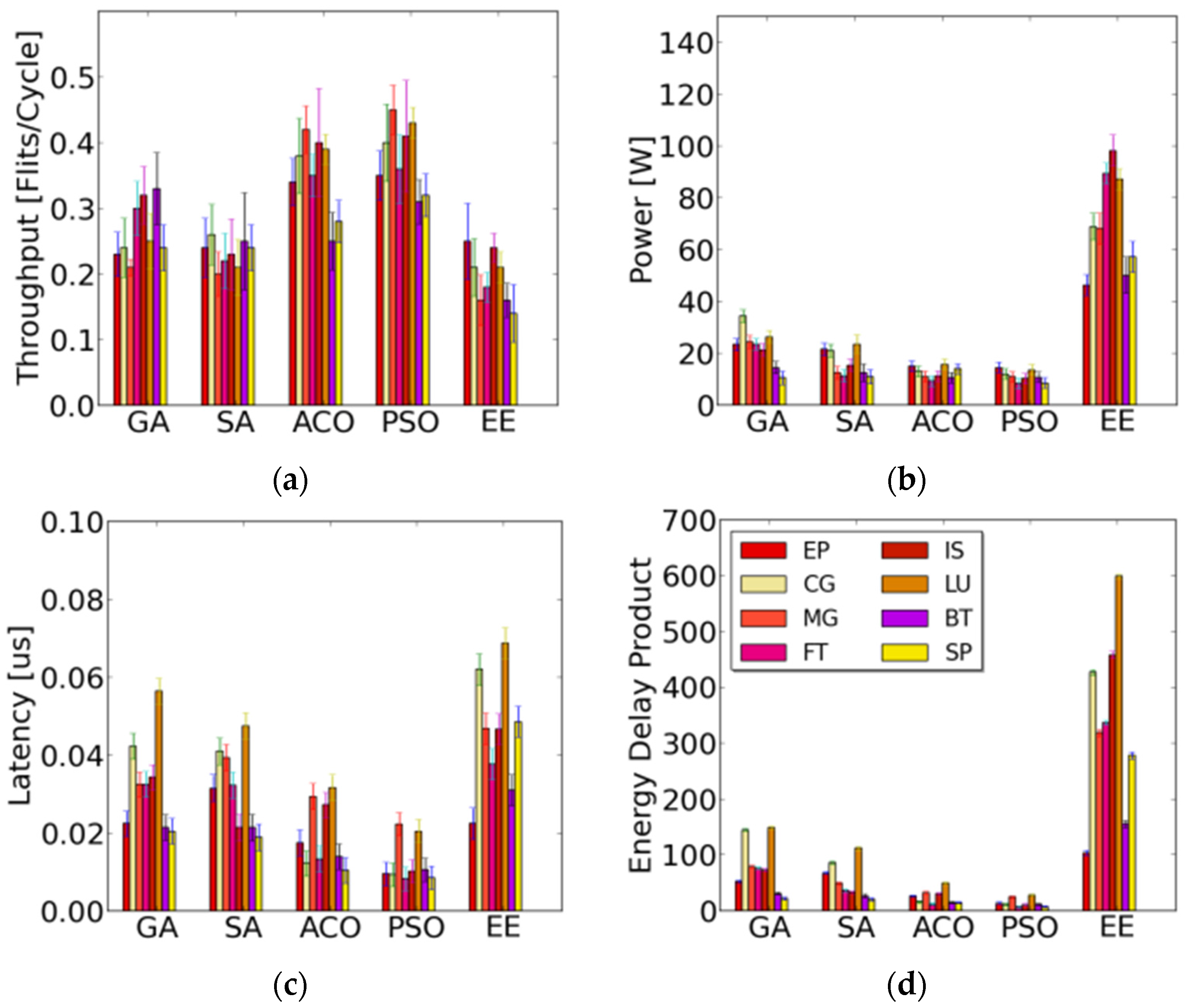
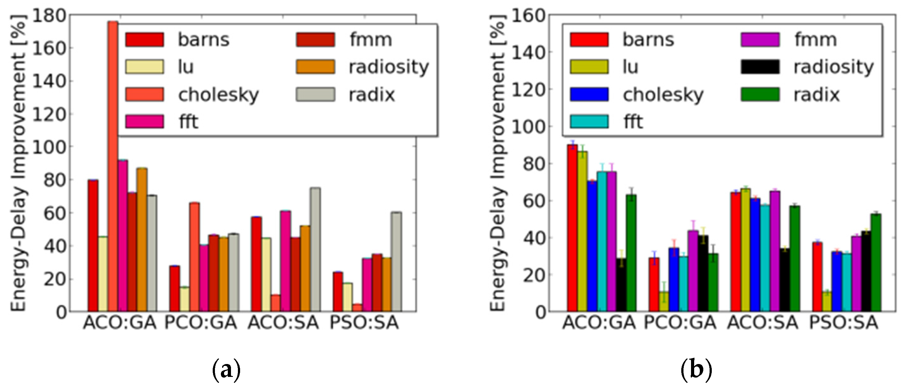
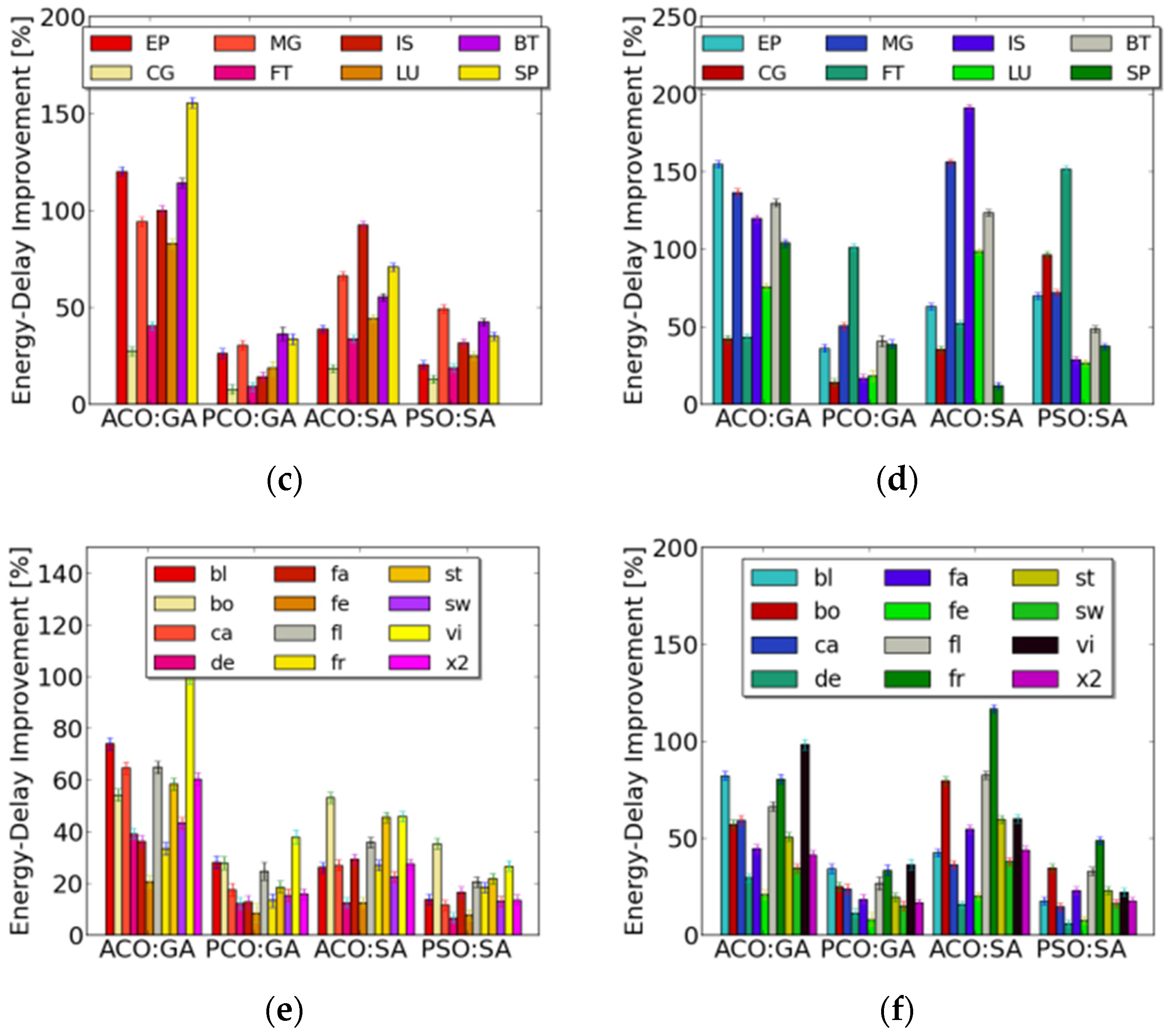
In this subsection, we present details of each of the four NoC synthesis heuristics based on Particle Swarm Optimization (PSO), Ant Colony Optimization (ACO), Simulated Annealing (SA), and Genetic Algorithm (GA) that we utilize to perform hybrid photonic NoC synthesis.

5.2.1. Particle Swarm Optimization (PSO)

The Particle Swarm Optimization (PSO) metaheuristic was initially proposed by R. Eberhart and J. Kenned [16] in 1995. The fundamental idea behind PSO is inspired by the coordinated and collective social behavior of species such as a flock of birds, fish, termites, or even humans. In nature, each individual bird, bee, or fish shares some information with its neighbors and by utilizing shared information collectively, they strive to organize efforts such as developing flying patterns to minimize aerodynamic drag, etc. Although by itself, a single entity such as a bird or a bee is a simple and unsophisticated creature, collectively as part of a swarm they can perform complex and useful tasks such as building nests, and foraging. Within the PSO framework, an individual entity is called a particle and it shares information with other particles, either in the form of direct or indirect communication to coordinate their problem-solving activities. In recent years, the PSO algorithm has been applied to many combinatorial optimization problems such as optimal placement of wavelength converters in WDM networks [38] and reconfiguration of field-programmable analog circuits [39].
To implement the PSO algorithm, particles are placed in the search space of some problem, and each particle evaluates the objective function at its current location to determine its next movement by combining the best (best-fitness) locations in the vicinity. The next iteration takes place after all particles are relocated to the new position. This process is repeated for all particles and eventually for the swarm as a whole. A particle on its own does not have the power to solve the problem; rather the solution evolves as the particles interact and work together, utilizing a social network consisting of bidirectional communication. As the algorithm iterates, particles move towards local as well as global solution optima forming a swarm pattern. For example, when one particle or entity finds a good solution, other particles in the vicinity are likely to be attracted to it. This social interaction feedback eventually causes all particles to move towards a globally optimal solution path. The phenomenon is similar to the social interactions where a leader or a set of leaders emerge from the swarm and followers attempt to follow them. In summary, the key idea in PSO is to mimic the social collective behavior found in nature and utilizing it to solve complex problems.
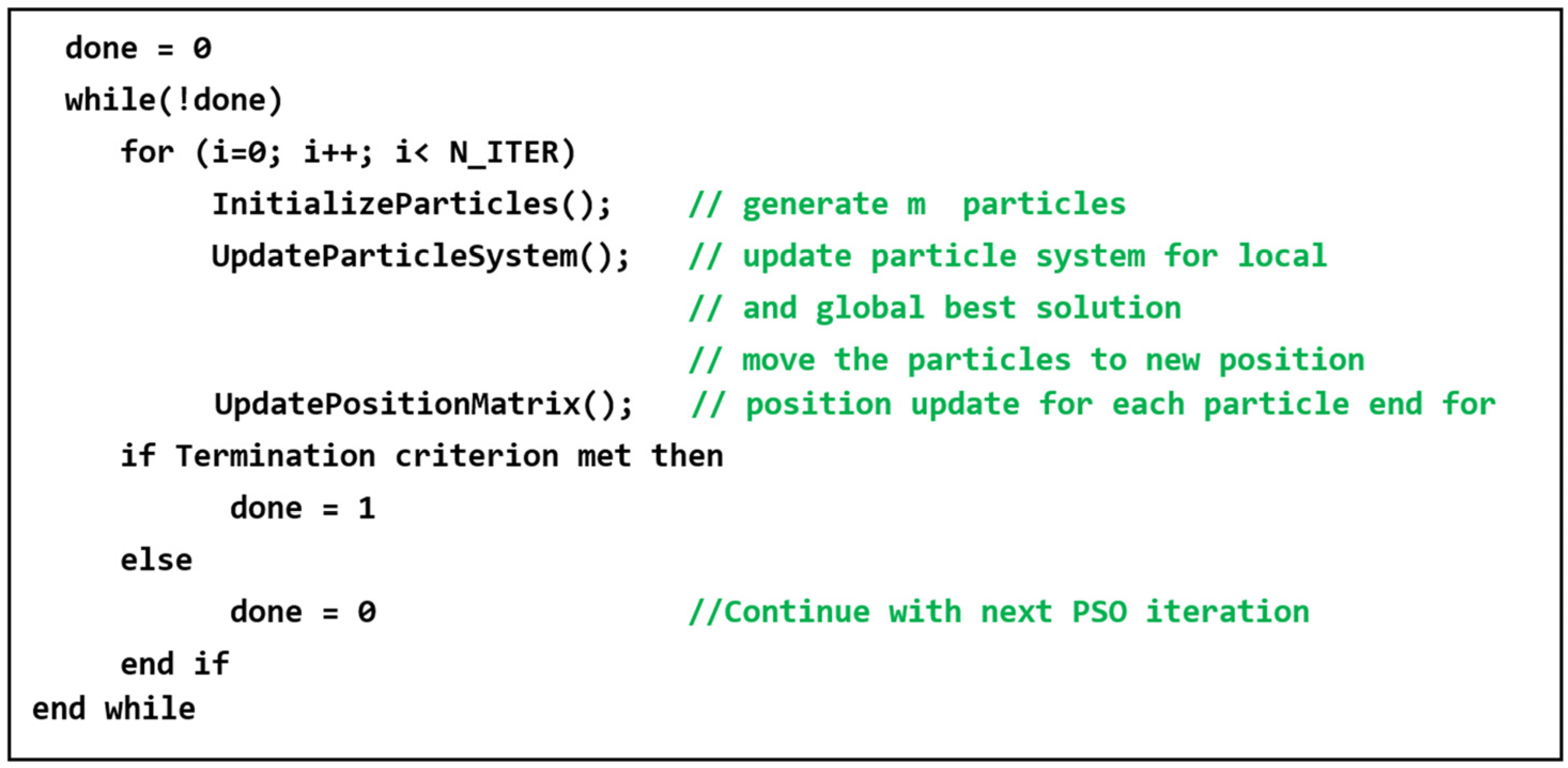
Figure 3 shows the pseudo-code for our PSO formulation, for the hybrid photonic NoC synthesis problem. The algorithm starts by initializing each particle with the function call InitializeParticles(). This function initializes inertia and learning weights (as discussed later in the section), and initial position and velocity for each parameter from Table 1. The UpdateParticleSystem() function iterates and updates velocity and positions of the individual particles, using relations (1) and (2) that are presented later in this section. At the end of the evaluation loop, particle positions are updated and they are moved to new positions by calling the UpdatePositionMatrix() function. This process continues for the application, until a dominating (global) solution emerges.
In our adaptation of the PSO algorithm for the hybrid photonic NoC synthesis problem, a particle represents a unique communication request from a source to a destination. A group of particles or solutions are initialized at the beginning of the PSO execution and then the optimal or near optimal solution is constructed using an iterative process. The PSO algorithm selects among various values for the parameters in Table 1 for each particle. Gradually one dominant solution emerges. This best configuration has a unique value for each of the parameters in Table 1, and satisfies application-specific latency constraints, while minimizing power.
Within an iteration, a particle tracks the personal best solution (pk), which is the best solution found by the particle k, and the global best solution (gk), which is the best solution that was found by the entire population. Every particle moves towards the better solutions with some velocity and position. The computation step includes some amount of randomness instead of following an exact profile. This randomness can produce a superior solution, which may result in other particle being attracted towards it. In our implementation of the PSO algorithm, each particle updates its velocity and position based on the following set of equations:
v k + 1 = w v k + c 1 r 1   ( p k x k ) + c 2 r 2   ( g k x k )
x k + 1 = x k + v k + 1
where, the current velocity and position for each particle is defined by vk and xk respectively; pk represents the current best solution based on particle k’s history and gk defines the current best solution based on the entire population or swarm. The positive inertial weight w is assigned to control how fast or slow each particle can move based on its own weight or inertia, c1 and c2 are constant numbers that represent learning weights to control the learning rate of global vs. local optima, i.e., the higher the weight, the faster the particles gravitate towards the solution. Instead of just following the current best solution in a linear path, r1 and r2 are random numbers from 0 to 1 that change every iteration, adding randomness to the path, thus finding newer and better solutions on the way.
The stability of the PSO algorithm is one of the key concerns during implementation, where position and velocity can diverge instead of achieving convergence. To ensure solution convergence in our implementation, we tune the learning and inertial weights carefully and also implement a velocity limit parameter Vmax, where if the updated velocity exceeds the velocity limit, we saturate the velocity value to Vmax.

5.2.2. Ant Colony Optimization (ACO)

The Ant Colony Optimization (ACO) metaheuristic was proposed by Colorni, Dorigo, and Maniezzo [17] with the fundamental idea inspired by the behavior of real ants, specifically, the way they organize efforts to collect food. ACO is a probabilistic technique for solving computational problems which can be reduced to finding good paths through graphs. In recent years, this algorithm has been applied to many combinatorial optimization problems such as the asymmetric traveling salesman problem [31] and the graph coloring problem [32].
Although by itself, an ant is a simple and unsophisticated creature, collectively a colony of ants can perform useful tasks such as searching for food. Ants achieve stigmergic communication by laying down a chemical substance called pheromone, which can be sensed by other ants. When a pheromone trail laid by an ant that has found food is discovered by other ants, they tend to stop moving randomly and start following this specific trail, returning and reinforcing it if they eventually find food. Over time however, the pheromone trail starts to evaporate, thus reducing its attractive strength. The more time it takes for an ant to travel down the path and back again, the more time the pheromones have to evaporate. A short path, by comparison, gets marched over more frequently, and thus the pheromone density becomes higher on shorter paths than longer ones. Pheromone evaporation is crucial for avoiding the convergence to a locally optimal solution. If there were no evaporation at all, the paths chosen by the first ants would tend to be excessively attractive to the following ones. In that case, the exploration of the solution space would be constrained. The key idea of our ACO based hybrid photonic NoC synthesis algorithm is to mimic this behavior with “simulated ants” walking around a graph representing the problem to solve.
An ant in our formulation can be thought of as a simple computational agent that helps iteratively construct a solution for our synthesis problem. The intermediate solutions are referred to as solution states. At each iteration of the algorithm, an ant k moves probabilistically from a state i to state j. Each of the parameters from Table 1 has a separate evaporation trail value (τij) that represents the amount of pheromone deposited for a state transition between i and j. The selection probability for a parameter is a function of its attractiveness η i j β , defined by inverse of normalized power consumption for parameter β. Global convergence within the selection process is achieved by increasing attractiveness η i j β for low power dissipation solutions that meets latency constraints.
An empirically-derived pheromone evaporation coefficient (ρ) with a value 1 > (ρ) > 0 is utilized to control the evaporation of a trail over time. Trails are updated usually when all ants have completed their solution, increasing or decreasing the value of trails corresponding to moves that were part of “good” or “bad” solutions, respectively. Δτij represents the change in trail value based on the choices available for a parameter, and the impact they have on the cost function (in our case power dissipation). At the start of simulation, selection probability of each parameter is equal. If power dissipation reduces significantly based on a parameter change for a majority of the communications, then Δτij increases which causes the resulting selection probability to also increase. The selection for each parameter is performed using the following rules:
τ i j ( t + n ) = ρ * τ i j ( t ) + Δ τ i j
which is the trail update relation, with Δτij given by:
Δ   τ i j = k = 1 m Δ   τ i j k
for all m ants. The probability p i j k of moving from state i to j for the kth ant is given as:
p i j k = τ i j α   ( t )   η i j β   ( t ) τ i j α   ( t )   η i j β   ( t )
This probability depends on the attractiveness η i j β of the move computed based on increasing a tunable weight for an ant for which power is lower and latency is within the constraints, and the trail level τij of the move, indicating how proficient it has been in the past to make that particular move. α ≥ 0 is a parameter to control the influence of τij, and β ≤ 1 controls the influence of ηij.
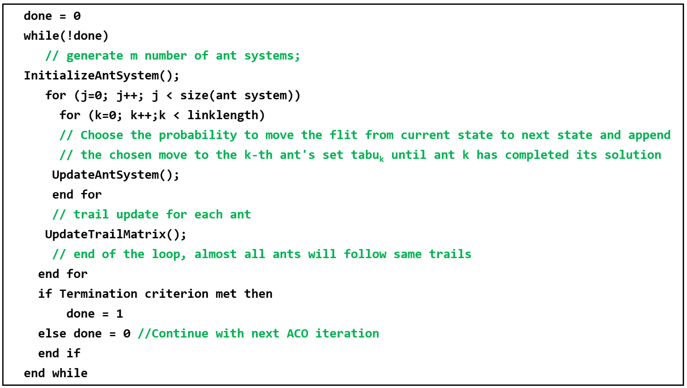
Figure 4 shows the pseudo-code for our ACO formulation to solve the hybrid photonic NoC synthesis problem. The algorithm starts by calling InitializeAntSystem() to initialize the ant system, with each ant representing a unique communication trace between a pair of cores. The function also sets up equal selection probability for every parameter. The function UpdateAntSystem() updates the probabilities of the individual ants, using Relations (3), (4), and (5). If the source core lies within a PRI region, the flow (ant) is directed towards the nearest gateway interface. The state transition parameter selection probability p i j k is applied to select serialization degree, clock frequency, flit width, and PRI data threshold. Once a flit reaches the uplink, number of waveguides and WDM density are selected for the next state. The same process is repeated for the destination gateway interface and destination core. As ants reach the destination, trail values are updated based on Equations (4) and (5), improving selection probability of parameters that lead to lower power dissipation. At the end of the evaluation loop, the trail and pheromone updates are performed by calling UpdateTrailMatrix(). This process continues until a dominant solution emerges.

5.2.3. Simulated Annealing (SA)

Simulated Annealing (SA) algorithms [14,41,42] generate solutions to optimization problems using techniques inspired by annealing in solids. SA algorithms simulate the cooling of a metal in the heat bath known as annealing where the structural properties depend on the cooling rate. When a metal is hot and in liquid state, if cooled in a controlled fashion, large and consistent grains can be formed. On the other hand, grains may contain imperfections if the liquid is quenched or cooled rapidly. The key idea in SA algorithms is that by slowly lowering the temperature, globally optimal solutions can be approached asymptotically. SA allows hill climbing (i.e., moves with inferior quality) to be taken within the initial part of the iteration process to escape local minima.
An SA algorithm involves the evolution of an individual solution over a number of iterations, with a fitness value used for evaluating solution quality whose determination is problem dependent. Based on the law of thermodynamics, at temperature t the probability of an increase in energy of magnitude δE is given by:
P ( δ E ) = e ( δ E k t )
where k is the Boltzmann’s constant. This equation is directly applied to SA by dropping the Boltzmann constant which was only introduced into the equation to cope with different materials. The probability of accepting a state in SA is:
P = e ( c t )   < r
where r is a random number between 0 and 1, c defines the change in evaluation function output, t defines current temperature which is decremented at every iteration by a regression algorithm involving a linear method t(k+1) = α.t(k), where α < 1 (our chosen value for α is presented in the Experimental Setup section (Section 6.1)). At each iteration, values for individual parameters (from Table 1) are selected randomly for the current solution and the probability of accepting the solution is determined by Equation (7). A high enough starting temperature (T0) is selected to allow movement through the entire search space. As the algorithm progresses, the temperature is cooled down to confine solutions, allowing better solutions to be accepted until the final temperature is reached. As SAs are heuristics, the solution found is not always guaranteed to be optimal. However in practice, SA has been used successfully to generate high quality solutions in several problem domains.
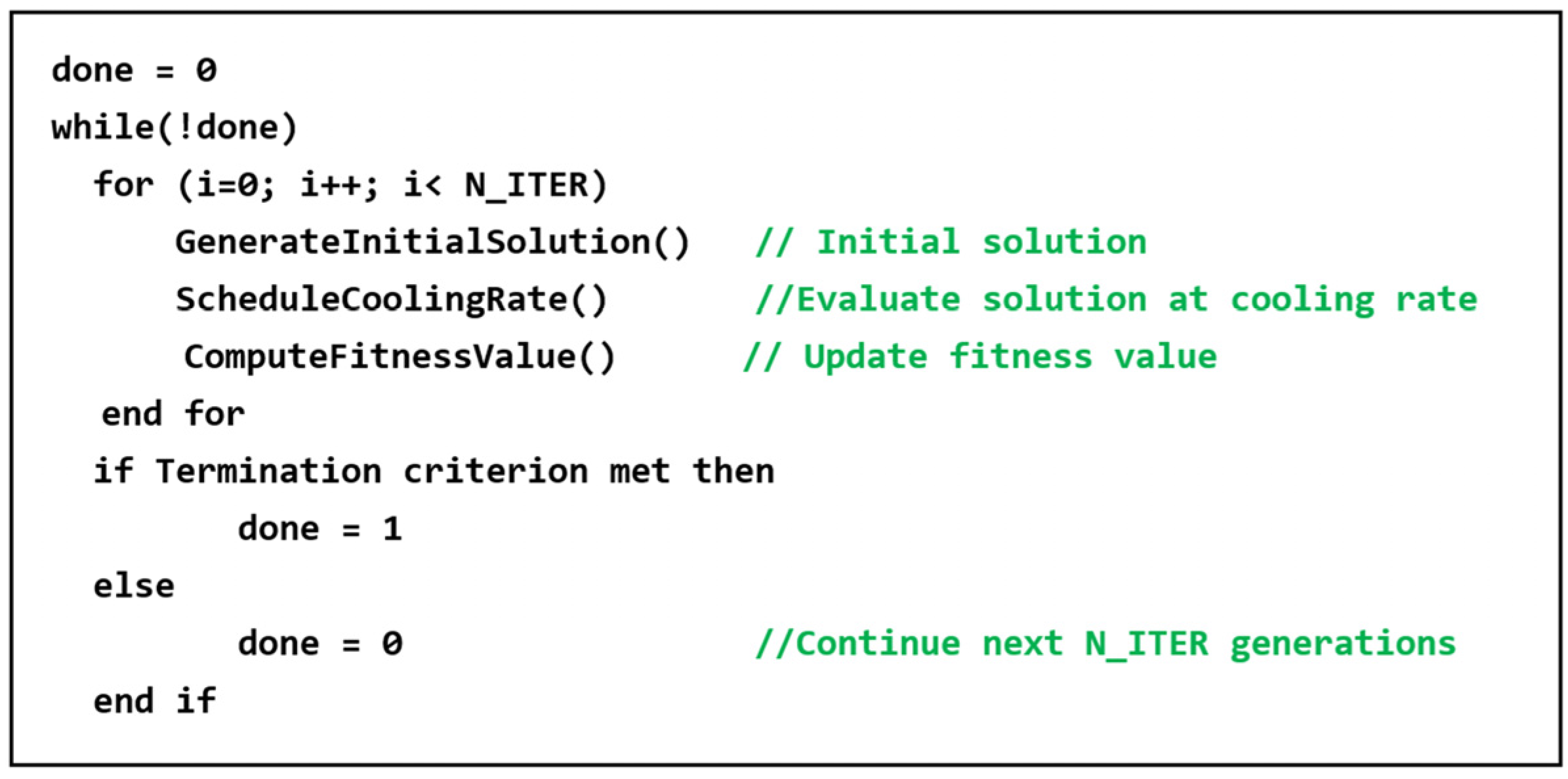
Figure 5 shows the pseudo-code of our SA formulation for the hybrid photonic NoC synthesis problem. Our SA implementation begins by calling GenerateInitialSolution() to generate an initial solution, where parameters from Table 1 in the solution are populated with randomly chosen valid values. Subsequently, four key parameters for annealing are initialized by calling ScheduleCoolingRate(): (i) Starting temperature; (ii) Temperature decrement; (iii) Final temperature, and (iv) Iterations at each temperature. We tuned the starting temperature to be hot enough to allow our hybrid photonic NoC synthesis parameters to traverse farther along in the solution space. Without this consideration, the final solution would be very close to the starting SA solution. Based on the number of iterations for which the algorithm will be running, the temperature needs to be decremented such that it will eventually arrive at the stopping criterion. We also need to allow enough iterations at each temperature such that the system stabilizes at that temperature. We evaluated a method first suggested in [43] that proposes implementing one iteration at each temperature by decreasing the temperature very slowly. The formula we used was t(k+1) = t(k)/(1 + βt(k+1)) where β is a suitably small value as defined in [43]. However the approach did not yield any benefits in terms of improvement in results. The fitness value is updated by calling ComputeFitnessValue(), and the process continues until temperature decays below a certain threshold or a predefined number of iterations have passed. The fitness value we use in our SA algorithm is a weighted combination of average packet latency and communication power dissipation.

5.2.4. Genetic Algorithm (GA)

Genetic algorithms (GAs) [15] generate solutions to optimization problems using techniques inspired by natural evolution, such as inheritance, mutation, selection, and crossover. A GA involves the evolution of a population of individuals over a number of generations. Each individual of the population is assigned a fitness value whose determination is problem dependent. At each generation, individuals are selected for reproduction based on their fitness value. Such individuals are crossed to generate new individuals, and the new individuals are mutated with some probability.
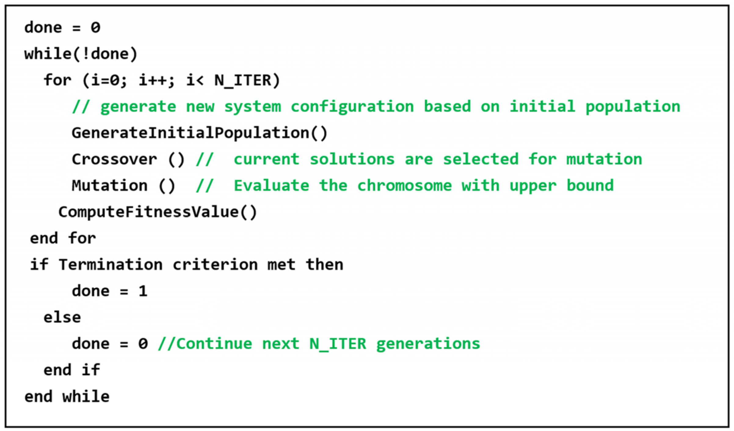
Figure 6 shows the pseudo-code of the GA formulation for our hybrid photonic NoC synthesis problem. Our GA implementation begins with the generation of an initial population by calling GenerateInitialPopulation(). Each individual element of this population consists of a chromosome with constituent parameters as defined in Table 1. Thus, each chromosome in the population represents a unique solution to our hybrid photonic NoC synthesis problem. Based on empirical analysis, we set our GA population size to 2000, composed of chromosomes with parameter values set according to a uniform random distribution. The fitness value assigned to each chromosome consists of a weighted combination of average packet latency and communication power dissipation. The fitness is evaluated analytically based on the communication requirements of the application for which the hybrid NoC is being synthesized. Each application can have a unique set of communication patterns (represented by edges in the core graph), and thus the same architectural optimization (e.g., changing PRI size) can impact the latency and power dissipation of different applications differently.
Similar to a roulette wheel, a probability based selection process was implemented for choosing chromosomes from the population to perform crossover and mutation on. Crossover was applied to randomly paired parameters of selected chromosome pairs by exchanging genetic information via swapping bits within the parent’s chromosome (by calling Crossover()). We also implemented multipoint crossovers where multiple parts of chromosome strings replaced each other. Then mutation was performed by calling Mutation(), where one parameter was changed within allowable limits (as defined in Table 1). Mutations and crossovers produced the chromosomes for the next generation, and the process continues iteratively till a termination criteria is met.
As GA is a stochastic search algorithm, it is difficult to formally specify convergence criteria based on optimality. The results are expected to get better with every generation, however sometimes the fitness of a population, calculated by calling ComputeFitnessValue(), may remain unchanged for a number of generations before any superior chromosomes can be created. The general practice is to terminate the GA after a predefined number of generations and then to evaluate the quality of the results within the population against the expected optimal, where expected optimal is obtained using extended GA runs or iterations.

5.3. Cycle Accurate Simulation and Validation

Upon completion of the synthesis algorithms (PSO, ACO, SA, and GA), we verified the results obtained from these algorithms using an in-house SystemC-based [44] cycle-accurate hybrid photonic NoC simulator. This was done to ensure that latency constraints are satisfied in the presence of communication congestion and computation delays, which can only be accurately analyzed via simulation. If the cycle-accurate simulation found a generated solution that violated the communication latency constraints, it was pruned out from the final solution set. If all solutions generated by an algorithm that meet performance constraints are pruned away, this step will lead to the re-invocation of the algorithm. As all the search algorithms considered in our work involve some measure of random search, such a step would ensure that a different set of outputs are generated across different invocations of the search algorithms.

6. Experiments

6.1. Experimental Setup

We conducted extensive experimental analysis to compare the performance of our PSO, ACO, GA and SA based hybrid photonic NoC synthesis frameworks for mid-size 6 × 6 (36-core) and large-size 10 × 10 (100-core) CMPs with a 2D mesh hybrid photonic ring/mesh NoC fabric. Parallel implementations of seven SPLASH-2 benchmarks [45] (barnes, lu, cholesky, fft, fmm, radiosity, radix) were utilized to guide the application-specific synthesis. We also utilized NAS [46] and PARSEC [47] parallel application benchmarks. NAS [46] benchmarks are derived from computational fluid dynamics (CFD) applications. The Princeton Application Repository for Shared-Memory Computers (PARSEC) [47] suite is composed of several multithreaded programs that represent next-generation shared-memory programs for CMPs. Our synthesis runs lasted around 8 to 10 h for each search algorithm; however initial runs lasted around 4–6 days. Once we realized that 8–10 h of runtime was able to provide solutions with performance within 2%–4% of solutions generated with extended runs, we reduced our simulation time to be more efficient.
We targeted a 32 nm process technology with the assumption of a 400 mm2 die area budget. Table 2 shows delay values for 32 nm technology that we assumed, obtained from [48] and from device fabrication results [49]. The delay of an optimally repeated and sized copper wire at 32 nm was assumed to be 42 ps/mm [50]. The power dissipated in the hybrid photonic NoC can be categorized into (i) electrical network power and (ii) photonic ring network power. The static and dynamic power dissipation of electrical routers and links were derived from Orion 2.0 [51]. For the energy dissipation of the modulator driver and TIA power we used ITRS device projections [1] and circuit-level implementation results. Energy dissipation values for the photonic modulators and receivers are also summarized in Table 2. An off-chip electrical laser power of 3.3 W (with 30% efficiency) is also considered in our energy calculations. The laser power value accounts for per component optical losses due to various factors such as non-linearity (1 dB at 30 mW), couplers/splitters (1.2 dB), waveguides (3 dB/cm), waveguide crossings (0.05 dB), ring modulators (1 dB), receiver filters (1.5 dB) and photodetectors (0.1 dB).
The search heuristics were configured as follows. For the PSO algorithm, we empirically set the inertia weight w = 0.66, c1 = c2 = 0.5, and the velocity limit parameter Vmax = 0.33. For the ACO algorithm, we set the pheromone evaporation coefficient ρ = 0.67, and tunable weights α and β were set to 0.46 and 0.54, respectively. For the SA algorithm, we set α to 0.997, and utilized initial temperature T0 = 1000 °C. For the GA, we maintained an initial population size of M = 256 ( N × N ) 2 where N is the (X or Y) mesh dimension of the NoC and ran the algorithm for up to 2000 generations. We evaluated our GA implementation for various mutation and crossover probabilities and ultimately utilized values of 0.3 and 0.2, respectively.

6.2. Results

Our first experiment provides insights into the workings of the PSO and ACO algorithms. Figure 7 shows the solution space pre- and post-PSO and ACO, that compares the power and average packet latency, for the lu benchmark from the SPLASH-2 suite. The solution space is relatively randomly distributed in 2D with higher power consumption before the PSO and ACO algorithms begin execution. The ACO solutions converge towards the shortest path (lower left quadrant) of the 2D space as can be seen in Figure 7b. This result can be explained based on Equation (5), as the attractiveness of shortest paths grows higher in the ACO algorithm over time. On the other hand, the PSO algorithm drives the solutions more uniformly towards lower power as can be seen in Figure 7a by following velocity/position profiles relative to local and global minimum power solutions.
To gain insights into the quality of the generated solutions using different search techniques, we evaluated the best solutions (lowest power solutions that meet application latency constraints) generated by ASO, PSO, GA and SA for the seven SPLASH-2 benchmarks. Figure 8 shows results for the 10 × 10 CMP while Figure 9 presents results on a 6 × 6 CMP implementation. For reference purposes, we also show the results for a purely electrical regular 2D NoC without any customization (EE). On average it can be seen that ACO and PSO algorithms generate solutions with lower power, lower latency, and lower energy delay product (EDP), as well as higher throughput than the best solutions generated by the SA and GA algorithms.
In summary, from the results in Figure 8 and Figure 9, it can be seen that despite the overhead of additional photonic components, using hybrid photonic NoCs can lead to orders of magnitude savings in power dissipation over electrical NoCs. Among the synthesis algorithms considered, the solutions generated with PSO and ACO have as much as 1.2× lower power dissipation on average than solutions generated by SA and GA (with 2.2× power savings for the best case).
Table 3, Table 4, Table 5 and Table 6 summarize the synthesis parameter values for the best solutions generated by the PSO, ACO, SA, and GA algorithms, for SPLASH-2 benchmark applications implemented on the 10 × 10 hybrid photonic NoC. The communication traffic pattern for each benchmark is different, so these results provide insights into the inner workings of each of the synthesis algorithms. Both ACO and PSO achieve a higher photonic path utilization (as can be observed from their higher WDM, PRI, and uplink count values) compared to SA and GA, especially for benchmarks with high communication load (e.g., radix). In fact, the superior results obtained with PSO and ACO can be explained by looking at many of the selected parameter values for the solutions, which are similar. Among ACO and PSO, it was found that ACO generated solutions with lower latency on average than PSO. This can be explained by looking at the PRI data threshold values for the two approaches. ACO has larger PRI data threshold values than PSO (particularly for the radiosity, fmm and radix benchmarks), indicating that ACO generated solutions that utilized photonic links only for large data transfer sizes when it is most efficient to use photonic links, whereas smaller sized data transfers used the electrical NoC. The chosen PRI data threshold values led to a better load balancing between photonic and electrical paths, resulting in ACO outperforming PSO by a small margin.
Figure 10 and Figure 11 present the best solutions generated by the algorithms for the PARSEC benchmarks, while Figure 12 and Figure 13 present results for NAS benchmarks. For both sets of benchmark applications, the ACO and PSO algorithms achieve superior solutions than SA and GA, similar to the trend observed with SPLASH-2 benchmarks in Figure 8 and Figure 9.
Figure 14 summarizes the energy-delay product (EDP) improvements for the best solutions generated with the PSO and ACO algorithms, compared to the GA and SA algorithms. The adaptation of the PSO search algorithm to our hybrid photonic NoC synthesis problem generated solutions that achieved on average 64% EDP improvements over GA and 53% improvements over SA. Our adaptation of the ACO algorithm achieved on average 107% EDP improvements over GA and 62% improvements over SA. We also observed significant (up to 18×) improvements in EDP with PSO and ACO generated hybrid photonic NoC solutions compared to the baseline 2D electrical mesh NoC architecture, for the given application benchmarks. Thus, our proposed algorithmic synthesis framework is an effective software tool to rapidly prototype high quality hybrid photonic NoC architectures for future CMPs.
Lastly, we discuss the area overhead of our customized hybrid photonic NoC architecture. Based on our analysis of a 10 × 10 electrical torus, electrical mesh, Corona [7], Firefly [8], and our proposed hybrid photonic NoC architecture, these architectures on average have a 16.33, 14.46, 1.78, 3.39, 18.1 mm2 electrical area overhead respectively and photonic area overheads of 0, 0, 223, 147, 67 mm2 respectively. It can be seen that our proposed architecture has a higher electrical-layer area footprint compared to the other architectures. This area is greater than the electrical mesh area primarily due to the extra router complexity at the gateway interfaces. Firefly and our proposed architecture both have lower area overhead than Corona, which uses significantly higher number of resonators and detector resources. Our proposed architecture also has a lower optical-layer area overhead compared to Firefly, which uses a more complex optical crossbar.

7. Conclusions

In this article, we proposed a framework for rapidly synthesizing hybrid photonic NoC architectures for emerging CMPs. We formulate the synthesis problem using four different search heuristics: Particle Swarm Optimization (PSO), Ant Colony Optimization (ACO), Simulated Annealing (SA) and Genetic Algorithms (GA). One of our goals in this work was to evaluate and determine the appropriate algorithm that provides the best quality solutions. Our results and experimental data demonstrate significant promise for the ACO as well as PSO-based search algorithms for our problem domain of hybrid photonic NoC synthesis, allowing us to determine application-specific architectural parameters that minimize power dissipation while satisfying application latency constraints.

Acknowledgments

This research is supported by grants from Semiconductor Research Corporation (SRC), National Science Foundation (NSF) (CCF-1252500, CCF-1302693), and Air Force Office of Scientific Research (AFOSR) (FA9550-13-1-0110).

Author Contributions

Shirish Bahirat and Sudeep Pasricha conceived and designed the experiments; Shirish Bahirat performed the experiments; Shirish Bahirat and Sudeep Pasricha analyzed the data; Shirish Bahirat and Sudeep Pasricha wrote the paper.

Conflicts of Interest

The authors declare no conflict of interest.

References

  1. ITRS Technology Working Groups. International Technology Roadmap for Semiconductors (ITRS). 2007. Available online: http://public.itrs.net (accessed on 2 December 2016).
  2. Benini, L.; De-Micheli, G. Networks on Chip: A new SoC paradigm. Computer 2002, 49, 70–71. [Google Scholar] [CrossRef]
  3. Goodman, J.; Leonberger, F.; Kung, S.-Y.; Athale, R. Optical interconnects for VLSI systems. Proc. IEEE 1984, 72, 850–866. [Google Scholar] [CrossRef]
  4. Chen, G.; Chen, H.; Haurylau, M.; Nelson, N.; Fauchet, P.M.; Friedman, E.G.; Albonesi, D. Predictions of CMOS compatible on-chip optical interconnect. In Proceedings of the 2005 International Workshop on System Level Interconnect pRediction, San Francisco, CA, USA, 2–3 April 2005; pp. 13–20.
  5. Le Beux, S.; Li, H.; O’Connor, I.; Cheshmi, K.; Liu, X.; Trajkovic, J.; Nicolescu, G. Chameleon: Channel efficient Optical Network-on-Chip. In Proceedings of the conference on Design, Automation & Test in Europe, Dresden, Germany, 24–28 March 2014; pp. 1–6.
  6. Le Beux, S.; Li, H.; Nicolescu, G.; Trajkovic, J.; O’Connor, I. Optical crossbars on chip, a comparative study based on worst-case losses. Concurr. Comput. Pract. Exp. 2014, 26, 2492–2503. [Google Scholar] [CrossRef]
  7. Vantrease, D.; Schreiber, R.; Monchiero, M.; McLaren, M.; Jouppi, N.; Fiorentino, M.; Davis, A.; Binkert, N.; Beausoleil, R.; Ahn, J. Corona: System implications of emerging nanophotonic technology. In Proceedings of the 35th Annual International Symposium on Computer Architecture, Beijing, China, 21–25 June 2008; pp. 153–164.
  8. Pan, Y.; Kumar, P.; Kim, J.; Memik, G.; Zhang, Y.; Choudhary, A. Firefly: Illuminating future network-on-chip with nanophotonics. In Proceedings of the 36th Annual International Symposium on Computer Architecture, San Diego, CA, USA, 3–5 December 2009; pp. 429–440.
  9. Shacham, A.; Bergman, K.; Carloni, L.P. The case for low-power photonic networks on chip. In Proceedings of the 44th Annual Design Automation Conference, San Diego, CA, USA, 4–8 June 2007; pp. 132–135.
  10. Bahirat, S.; Pasricha, S. METEOR: Hybrid Photonic Ring-Mesh Network-on-Chip for Multicore Architectures. ACM Trans. Embed. Comput. Syst. TECS. 2014, 13, 116:1–116:33. [Google Scholar] [CrossRef]
  11. Li, Z.; Fay, D.; Mickelson, A.; Shang, L.; Vachharajani, M.; Filipovic, D.; Park, W.; Sun, Y. Spectrum: A hybrid nanophotonic-electric on-chip network. In Proceedings of the 46th Annual Design Automation Conference, San Francisco, CA, USA, 26–31 July 2009; pp. 575–580.
  12. Joshi, A.; Batten, C.; Kwon, Y.; Beamer, S.; Shamim, I.; Asanovic, K.; Stojanovic, V. Silicon-Photonic clos networks for global on-chip communication. In Proceedings of the 2009 3rd ACM/IEEE International Symposium on Networks-on-Chip, San Diego, CA, USA, 10–13 May 2009; pp. 124–133.
  13. Morris, R.W.; Kodi, A.K. Power-efficient and high-performance multi-level hybrid nanophotonic interconnect for Multicores. In Proceedings of the 2010 Fourth ACM/IEEE International Symposium on Networks-on-Chip, Grenoble, France, 3–6 May 2010; pp. 207–214.
  14. Kirkpatrick, S.; Gelatt, C.D., Jr.; Vecchi, M.P. Optimization by simulated annealing. Science 1983, 220, 671–680. [Google Scholar] [CrossRef] [PubMed]
  15. Mazumder, P. Genetic Algorithms for VLSI Design, Layout and Test Automation; Prentice-Hall: Upper Saddle River, NJ, USA, 1999. [Google Scholar]
  16. Eberhart, R.; Kenned, J. A new optimizer using particle swarm theory. In Proceedings of the 6th International Symposium on Micromachine and Human Science, Nagoya, Japan, 4–6 October 1995; pp. 39–43.
  17. Dorigo, M.; Maniezzo, V.; Colorni, A. Ant system: Optimization by a colony of cooperating agents. IEEE Trans. Syst. Man Cybern. B 1996, 26, 29–41. [Google Scholar] [CrossRef] [PubMed]
  18. Goldberg, D. Genetic Algorithms in Search, Optimization and Machine Learning; Kluwer Academic Publishers: Boston, MA, USA, 1989. [Google Scholar]
  19. Bahirat, S.; Pasricha, S. A particle swarm optimization approach for synthesizing application-specific hybrid photonic networks-on-chip. In Proceedings of the 17th International Conference on Parallel Architectures and Compilation Techniques, Toronto, ON, Canada, 25–29 October 2012; pp. 78–83.
  20. Collet, J.H.; Caignet, F.; Sellaye, F.; Litaize, D. Performance constraints for onchip optical interconnects. IEEE J. Sel. Top. Quantum Electron. 2003, 9, 425–432. [Google Scholar] [CrossRef]
  21. Tosik, G.; Gaffiot, F.; Lisik, Z.; O’Connor, I.; Tissafi-Drissi, F. Power dissipation in optical and metallic clock distribution networks in new VLSI technologies. Electron. Lett. 2004, 40, 198–200. [Google Scholar] [CrossRef]
  22. Kobrinsky, M.; Block, B.; Zheng, J.-F.; Barnett, B.; Mohammed, E.; Reshotko, M.; Robertson, F.; List, S.; Young, I.; Cadien, K. On-chip optical interconnects. Intel Technol. J. 2004, 2, 129–142. [Google Scholar]
  23. Bahirat, S.; Pasricha, S. HELIX: Design and synthesis of hybrid nanophotonic application-specific network-on-chip architectures. In Proceedings of the Fifteenth International Symposium on Quality Electronic Design, Santa Clara, CA, USA, 3–5 March 2014; pp. 91–98.
  24. Wang, J.; Zhu, M.; Peng, C.; Zhou, L.; Qian, Y.; Dou, W. Software-defined photonic network-on-chip. In Proceedings of the 2014 Third International Conference on E-Technologies and Networks for Development (ICeND), Beirut, Lebanon, 29 April–1 May 2014; pp. 127–130.
  25. Browning, M.; Li, C.; Gratz, P.; Palermo, S. LumiNOC: A low-latency, high-bandwidth per Watt, photonic Network-on-Chip. In Proceedings of the 2013 ACM/IEEE International Workshop on System Level Interconnect Prediction (SLIP), Austin, TX, USA, 2 June 2013; pp. 1–4.
  26. Ahmed, A.; Meyer, M.; Okuyama, Y.; Abdallah, A. Hybrid Photonic NoC Based on Non-Blocking Photonic Switch and Light-Weight Electronic Router. In Proceedings of the 2015 IEEE International Conference on Systems, Man, and Cybernetics (SMC), Kowloon, Hong Kong, 9–12 October 2015; pp. 56–61.
  27. Pintus, P.; Gambini, F.; Faralli, S.; Pasquale, F.; Cerutti, I.; Andriolli, N. Ring Versus Bus: A Theoretical and Experimental Comparison of Photonic Integrated NoC. J. Lightwave Technol. 2015, 33, 4870–4877. [Google Scholar] [CrossRef]
  28. Li, Z.; Qouneh, M.; Joshi, M.; Zhang, W.; Fu, X.; Li, T. Aurora: A Cross-Layer Solution for Thermally Resilient Photonic Network-on-Chip. IEEE Trans. Very Large Scale Integr. VLSI Syst. 2015, 23, 173–183. [Google Scholar]
  29. Murali, S.; Micheli, G.D. Bandwidth-Constrained Mapping of Cores onto NoC Architectures. In Proceedings of the Conference on Design, Automation and Test in Europe, Paris, France, 16–20 February 2004; Volume 2, pp. 896–901.
  30. Ascia, G.; Catania, V.; Palesi, M. Multi-objective mapping for mesh-based noc architectures. In Proceedings of the 2nd IEEE/ACM/IFIP International Conference on Hardware/Software Codesign and System Synthesis, Stockholm, Sweden, 8–10 September 2004; pp. 182–187.
  31. Hu, J.; Marculescu, R. Energy-aware mapping for tile-based noc architectures under performance constraints. In Proceedings of the 2003 Asia and South Pacific Design Automation Conference, Kitakyushu, Japan, 21–24 January 2003; pp. 233–239.
  32. Kapadia, N.; Pasricha, S. VISION: A framework for voltage island aware synthesis of interconnection networks-on-chip. In Proceedings of the 21st Edition of the Great Lakes Symposium on Great Lakes Symposium on VLSI, Lausanne, Switzerland, 2–4 May 2011; pp. 31–36.
  33. Murali, S.; Meloni, P.; Angiolini, F.; Atienza, D.; Carta, S.; Benini, L.; Micheli, G.D.; Raffo, L. Designing application-specific networks on chips with floorplan information. In Proceedings of the 2006 IEEE/ACM International Conference on Computer-Aided Design, San Jose, CA, USA, 5–9 November 2006; pp. 355–362.
  34. Kapadia, N.; Pasricha, S. A System-Level Cosynthesis Framework for Power Delivery and On-Chip Data Networks in Application-Specific 3-D ICs. IEEE Trans. Very Large Scale Integr. VLSI Syst. 2016, 24, 3–16. [Google Scholar] [CrossRef]
  35. Srinivasan, K.; Chatha, K.S. A low complexity heuristic for design of custom network-on-chip architectures. In Proceedings of the Conference on Design, Automation and Test in Europe, Munich, Germany, 6–10 March 2006; pp. 130–135.
  36. Chan, J.; Parameswaran, S. NoCOUT: NoC topology generation with mixed packet-switched and point-to-point networks. In Proceedings of the 2008 Asia and South Pacific Design Automation Conference, Seoul, Korea, 21–24 January 2008; pp. 265–270.
  37. Kwon, S.; Pasricha, S.; Jeonghun, C. POSEIDON: A framework for application-specific network-on-chip synthesis for heterogeneous chip multiprocessors. In Proceedings of the 2011 12th International Symposium on Quality Electronic Design (ISQED), Santa Clara, CA, USA, 14–16 March 2011; pp. 1–7.
  38. Teo, C.; Foo, Y.; Chien, S.; Low, A.; Venkatesh, B.; You, A. Optimal placement of wavelength converters in WDM networks using particle swarm optimizer. In Proceedings of the 2004 IEEE International Conference on Communications, Paris, France, 20–24 June 2004; pp. 1669–1673.
  39. Payet, M.; Fresse, V.; Rousseau, F.; Remy, P. Dynamic data flow analysis for NoC based application synthesis. In Proceedings of the International Symposium on Rapid System Prototyping (RSP), Amsterdam, The Netherlands, 8–9 October 2015; pp. 61–67.
  40. Romanov, A.; Romanova, I. Use of irregular topologies for the synthesis of networks-on-chip. In Proceedings of the 2015 IEEE 35th International Conference on Electronics and Nanotechnology, Kiev, Ukraine, 21–24 April 2015; pp. 445–449.
  41. Metropolis, N.; Rosenbluth, A.W.; Rosenbluth, M.N.; Teller, A.H.; Teller, E. Equations of state calculations by fast computing machines. J. Chem. Phys. 1953, 21, 1087–1092. [Google Scholar] [CrossRef]
  42. Černý, V. A thermodynamical approach to the travelling salesman problem: An efficient simulation algorithm. J. Optim. Theory Appl. 1985, 45, 41–51. [Google Scholar] [CrossRef]
  43. Lundy, M.; Mees, A. Convergence of an Annealing Algorithm. Math. Prog. 1986, 34, 111–124. [Google Scholar] [CrossRef]
  44. SystemC Initiative. Available online: http://www.systemc.org (accessed on 6 December 2015).
  45. Woo, S.C.; Ohara, M.; Torrie, E.; Singh, J.P.; Gupta, A. The SPLASH-2 programs: Characterization and methodological considerations. In Proceedings of the 22nd Annual International Symposium on Computer Architecture, Santa Margherita Ligure, Italy, 22–24 June 1995; pp. 24–36.
  46. Jin, H.; Frumkin, M.; Yan, J. The OpenMP Implementation of NAS Parallel Benchmarks and Its Performance; Technical Report NAS-99-011; NASA Ames Research Center: Mountain View, CA, USA, 1999. [Google Scholar]
  47. Bienia, C.; Kumar, S.; Singh, J.; Li, K. The PARSEC benchmark suite: characterization and architectural implications. In Proceedings of the 7th International Conference on Parallel Architectures and Compilation Techniques, New York, NY, USA, 25–29 October 2008; pp. 72–81.
  48. Barwicz, T.; Byun, H.; Gan, F.; Holzwarth, C.W.; Popovic, M.A.; Rakich, P.T.; Watts, M.R.; Ippen, E.P.; Kartner, F.X.; Smith, H.I.; et al. Silicon photonics for compact energy-efficient interconnects. J. Opt. Netw. 2007, 6, 63–73. [Google Scholar] [CrossRef]
  49. Hsieh, I.-W.; Chen, X.; Dadap, J.; Panoiu, N.; Osgood, R.; McNab, S.; Vlasov, Y. Ultrafast-pulse self-phase modulation and third-order dispersion in si photonic wire-waveguides. Opt. Express 2006, 14, 12380–12387. [Google Scholar] [CrossRef] [PubMed]
  50. Haurylau, M.; Chen, H.; Zhang, J.; Chen, G.; Nelson, N.; Albonesi, D.; Friedman, E.; Fauchet, P. On-chip optical interconnect roadmap: Challenges and critical directions. IEEE J. Sel. Top. Quantum Electron. 2006, 12, 1699–1705. [Google Scholar] [CrossRef]
  51. Kahng, A.; Bin, L.; Li-Shiuan, P.; Samadi, K. ORION 2.0: A fast and accurate NoC power and area model for early-stage design space exploration. In Proceedings of the 2009 Design, Automation and Test in Europe Conference (DATE), Nice, France, 20–24 April 2009; pp. 423–428.
Figure 1. Hybrid photonic ring-electrical mesh Network on Chip (NoC) architecture [10].
Electronics 05 00021 g001
Figure 2. NoC synthesis design flow of the synthesis process.
Electronics 05 00021 g002
Figure 3. Particle swarm optimization (PSO) formulation for hybrid photonic NoC synthesis.
Electronics 05 00021 g003
Figure 4. Ant Colony Optimization (ACO) formulation for hybrid photonic NoC synthesis.
Electronics 05 00021 g004
Figure 5. Simulate Annealing (SA) algorithm formulation for hybrid photonic NoC synthesis.
Electronics 05 00021 g005
Figure 6. Genetic Algorithm (GA) formulation for hybrid photonic NoC synthesis.
Electronics 05 00021 g006
Figure 7. lu benchmark power consumption and latency solution space (a) pre, post PSO (b) pre, post ACO.
Electronics 05 00021 g007
Figure 8. SPLASH-2 [45] benchmarks comparison for 10 × 10 NoC (a) throughput, (b) power, (c) latency and (d) energy delay product.
Electronics 05 00021 g008
Figure 9. SPLASH-2 [45] benchmarks comparison for 6 × 6 NoC. (a) throughput, (b) power, (c) latency, and (d) energy delay product.
Electronics 05 00021 g009
Figure 10. PARSEC [47] benchmarks comparison for 10 × 10 NoC (a) throughput, (b) power, (c) latency, and (d) energy delay product.
Electronics 05 00021 g010
Figure 11. PARSEC [47] benchmarks comparison for 6 × 6 NoC (a) throughput, (b) power, (c) latency, and (d) energy delay product.
Electronics 05 00021 g011
Figure 12. NAS [36] benchmarks comparison for 10 × 10 NoC. (a) throughput, (b) power, (c) latency, and (d) energy delay product.
Electronics 05 00021 g012
Figure 13. NAS [46] benchmarks comparison for 6 × 6 NoC. (a) throughput, (b) power, (c) latency, and (d) energy delay product.
Electronics 05 00021 g013
Figure 14. EDP improvements for solutions generated by ACO and PSO over SA and GA for (a) 6 × 6 SPLASH-2; (b) 10 × 10 SPLASH-2; (c) 6 × 6 NAS; (d) 10 × 10 NAS; (e) 6 × 6 PARSEC; (f) 10 × 10 PARSEC benchmarks.
Electronics 05 00021 g014aElectronics 05 00021 g014b
Table 1. Summary of Synthesis Parameters.
Synthesis ParametersRange LowRange High
Photonic Uplinks432
PRI1(num cores)/4
WDM Density32256
Searialization Degree132
Clock Frequency (GHz)16
PRI data size threshold (Mth)41024
Flit Width (bytes)4256
Waveguides2256
Table 2. Delay, energy of photonic elements (32 nm) [48].
ComponentDelayDDESETTE
Modulator Driver9.5 ps20 fJ/bit5 fJ/bit16 fJ/bit/heater
Modulator3.1 ps
Waveguide15.4 ps/mm---
Photo Detector0.22 ps20 fJ/bit20 fJ/bit16 fJ/bit/heater
Receiver4.0 ps
DDE = Data traffic dependent energy, SE = Static energy (clock, leakage), TTE = Thermal tuning energy (20 K temperature range).
Table 3. PSO Synthesis Results.
Synthesis Parametersbarnslucholeskyfftfmmradiosityradix
WDM681224483135132143
Uplinks44444812
PRI15121010121212
PRI Data Threshold9641204875496
Clock Frequency5454422
Source PRI Uplink9789899
Dest PRI Uplinks9999999
Flit Width432562885256128128
Serialization6193122
Waveguides18121351361122018
Table 4. ACO Synthesis Results.
Synthesis Parametersbarnslucholeskyfftfmmradiosityradix
WDM128561451385667166
Uplinks44444812
PRI4444888
PRI Data Threshold72325646186459148
Clock Frequency4245455
Source PRI Uplink44444812
Dest PRI Uplinks444445812
Flit Width28644649282842
Serialization12438121810
Waveguides483258108128128256
Table 5. Simulated Annealing Synthesis Results.
Synthesis Parametersbarnslucholeskyfftfmmradiosityradix
WDM10279581289314163
Uplinks4444444
PRI4444444
PRI Data Threshold176166096280459168
Clock Frequency4245654
Source PRI Uplink4444554
Dest PRI Uplinks5544554
Flit Width23648543261537
Serialization1143610177
Waveguides4822520010512890
Table 6. Genetic Algorithm Synthesis Results.
Synthesis Parametersbarnslucholeskyfftfmmradiosityradix
WDM897356896713067
Uplinks4444444
PRI4444444
PRI Data Threshold223234578139320123
Clock Frequency3333443
Source PRI Uplink4444444
Dest PRI Uplinks4444444
Flit Width28785643221238
Serialization11121311111211
Waveguides3525451789911189

