
Parallel Implementation of Lightweight Secure Hash Algorithm on CPU and GPU Environments

1
Department of Financial Information Security, Kookmin University, Seoul 02707, Republic of Korea
2
Department of Information Security, Cryptology, and Mathematics, Kookmin University, Seoul 02707, Republic of Korea
*
Author to whom correspondence should be addressed.
Electronics 2024, 13(5), 896; https://doi.org/10.3390/electronics13050896
Submission received: 31 October 2023
/
Revised: 13 February 2024
/
Accepted: 19 February 2024
/
Published: 26 February 2024
(This article belongs to the Special Issue Big Data and Cyber Security: Emerging Approaches and Applications)
Abstract
:Currently, cryptographic hash functions are widely used in various applications, including message authentication codes, cryptographic random generators, digital signatures, key derivation functions, and post-quantum algorithms. Notably, they play a vital role in establishing secure communication between servers and clients. Specifically, servers often need to compute a large number of hash functions simultaneously to provide smooth services to connected clients. In this paper, we present highly optimized parallel implementations of Lightweight Secure Hash (LSH), a hash algorithm developed in Korea, on server sides. To optimize LSH performance, we leverage two parallel architectures: AVX-512 on high-end CPUs and NVIDIA GPUs. In essence, we introduce a word-level parallel processing design suitable for AVX-512 instruction sets and a data parallel processing design appropriate for the NVIDIA CUDA platform. In the former approach, we parallelize the core functions of LSH using AVX-512 registers and instructions. As a result, our first implementation achieves a performance improvement of up to 50.37% compared to the latest LSH AVX-2 implementation. In the latter approach, we optimize the core operation of LSH with CUDA PTX assembly and apply a coalesced memory access pattern. Furthermore, we determine the optimal number of blocks/threads configuration and CUDA streams for RTX 2080Ti and RTX 3090. Consequently, in the RTX 3090 architecture, our optimized CUDA implementation achieves about a 180.62% performance improvement compared with the initially ported LSH implementation to the CUDA platform. As far as we know, this is the first work on optimizing LSH with AVX-512 and NVIDIA GPU. The proposed implementation methodologies can be used alone or together in a server environment to achieve the maximum throughput of LSH computation.
1. Introduction
Cryptographic hash functions play a crucial role in ensuring data integrity, facilitating message authentication codes, serving as key derivation functions, enabling digital signatures, functioning as deterministic random bit generators, and acting as pseudo-random number generators [1,2,3,4]. Moreover, these cryptographic hash functions find application in the National Institute of Standards and Technology (NIST) Post Quantum Cryptography (PQC) algorithm for the generation of pseudo-random values [5,6,7]. Various digital signature methods based on cryptographic hash functions exist, including Lamport signature, Winternitz One Time Signature (WOTS), the Merkle hash tree signature scheme, SPHINCS, and SPHINCS+ [8,9,10,11,12].
The Lightweight Secure Hash (LSH) is a cryptographic hash function characterized by a wide-pipe Merkle–Damgard structure [13]. Notably, LSH serves as a cryptographic algorithm integrated within the Korea Cryptographic Module Validation Program (KCMVP) framework [14]. Furthermore, LSH exhibits ease of implementation and achieves enhanced performance through the utilization of parallel processing instructions, such as SSE, AVX2, and NEON. Recent research has notably explored the design of SPHINCS+ digital signatures based on LSH [15].
Parallel computing represents a computational approach employing multiple processors or computing resources concurrently to address complex problems, thereby delivering heightened performance and processing speeds compared to single-processor systems [16]. Particularly advantageous for managing substantial datasets or computationally intricate tasks, parallel computing finds applications across diverse domains, encompassing scientific research, engineering applications, artificial intelligence, and graphics processing [17]. This paradigm is categorized into two principal types: Word-Level Parallelism, where multiple processors handle distinct tasks independently, minimizing dependencies between tasks; and Data Parallelism, wherein multiple processors collectively execute the same task to partition and process data [16]. This accelerates overall operations by subdividing data into smaller blocks and processing each block on a separate processor. Key concepts and technologies integral to parallel computing include multi-core processors, which embed multiple processor cores on a single chip to facilitate parallel processing; GPU (Graphics Processor Unit), originally designed for graphics processing but widely employed for scientific calculations and deep learning due to its robust parallel processing capabilities; and clusters and parallel computers, which interconnect independent computers to collaboratively tackle computational challenges. The parallel computing model encompasses the parallel programming model, a programming paradigm encompassing threading, interprocess communication, and message passing. Frameworks such as NVIDIA’s CUDA and Khronos Group’s OpenCL are instrumental tools and libraries facilitating the implementation of parallel computing on GPUs [18] While parallel computing offers substantial performance gains and efficiencies, a nuanced understanding of task dependencies is crucial. Employing appropriate tools and algorithms is essential for effective parallelization.
In the realm of network communication, servers interact with multiple clients, employing a variety of cryptographic algorithms for security protocols, including authentication, message integrity verification, and key exchange. The process of server/client authentication utilizes cryptographic-hash-function-based algorithms for message integrity verification and authentication, leading to a considerable number of hash function calls. As the server manages an increasing client load and handles numerous hash function calls, performance delays and heightened latency may become evident. To mitigate these challenges, this paper proposes the use of parallel computing with CPU SIMD and GPUs to reduce computational latency. This approach allows the server to parallelize authentication and message integrity verification processes, thereby optimizing performance. Furthermore, this paper introduces a design methodology for parallelizing LSH-512 operations using Intel CPU SIMD instruction set AVX-512. Additionally, parallel implementation methods for LSH-512/512 using NVIDIA CUDA C are suggested. The working process of LSH is analyzed, relevant AVX-512 instructions are identified, and a method to minimize memory access performance load in massively parallel message processing using GPU architecture is proposed.
The results of optimization research using AVX for various cryptographic algorithms (hash function, block cipher, Elliptic Curve Cryptography, PQC, etc.) have been published [19,20,21,22,23]. The study by Kim et al. is an optimal LSH implementation method using AVX-2 [19]. Kim et al. analyzed the SIMD instruction set and the LSH permutation process, and proposed efficient application methods [19]. In this way, various permutation types for LSH and SIMD were defined, enabling flexible implementation of LSH with new SIMD instruction sets for various register sizes or platforms [19]. However, the approach showed a relatively modest performance improvement of 5%.
Similar to AVX, research on cryptographic algorithm optimization using GPU architecture has been published. In the case of NIST PQC optimization research using GPU, various approaches were proposed, including a PQC internal function parallel method and a PQC internal function acceleration method using GPU Tensor Core [24,25,26,27,28,29,30]. In addition, research on ECC using GPU architecture is continuously being conducted [31,32,33]. Research on block cipher algorithms and hash functions in GPU architectures has also been published [34,35,36,37,38,39,40,41]. However, there are no studies of hash functions using AVX-512 and LSH optimization research implementation using GPUs. Therefore, an optimization study of the cryptographic hash function LSH is required.
The remainder of this article is organized as follows. Section 2 contains this article’s contributions. Section 3 defines the notation, LSH structure, and target platform used in the study. Section 4 includes our LSH-512 implementation methods using AVX-512, and Section 5 includes our LSH-512 parallel implementation using CUDA. Section 6 includes performance evaluations and analysis, and Section 7 contains the conclusions and discusses future work.
2. Contributions
In this section, we describe the contributions of our article. Our article’s contributions are as follows:
- Word-level parallel implementation methods of LSH-512 using AVX-512We executed LSH internal processes in parallel processing logic via AVX-512 instructions. We analyzed the 64-bit bitrate repetitive operations that occur in the LSH core function and, for the first time, designed AVX-512 processing logic to process them in parallel. We analyzed LSH compression process and proposed the first AVX-512-instruction-based implementation methods applicable to the compression process. To the best of our knowledge, this method has not previously been used or presented in the literature. Our implementation parallelizes the processing of message blocks and hash-chaining values during the compression process. Four AVX-512 registers are employed for parallelizing message block operations, while two AVX-512 registers are utilized for handling hash-chaining values. We further analyzed applicable AVX-512 instructions for internal operations, including permutation, and assessed the clock cost incurred during these internal operations. As a result, our LSH-512/512 implementation achieves a performance of 1.62 Clock Per Byte (CPB) for a 16 MB message. Notably, our first implementation demonstrates a performance improvement of up to 50.37% compared to other AVX-2-based LSH-512/512 implementations on the Intel Rocket Lake CPU device [42];
- Data parallel implementation methods of LSH-512 using CUDAWe designed logic to process LSH hash operations for multiple messages in parallel, leveraging GPU architecture resources. In other words, we leveraged CUDA to design the LSH data parallel processing logic. Additionally, we proposed a method to accelerate the LSH operation performed by each thread and efficiently handled performance bottlenecks that may occur in GPU architecture. In more detail, we proposed efficient memory handling methods for memory access in NVIDIA GPU architecture. We analyzed CUDA’s memory area and suggested several approaches to minimize memory load/store times. Specifically, we introduced a method to reduce the time of global memory accesses during command processing in CUDA warp units. Additionally, our implementation utilizes CUDA streams to minimize the performance overhead associated with memory access on GPU architectures through asynchronous operations. Finally, our LSH implementation is designed using PTX, a CUDA inline assembly. To the best of our knowledge, this method has not previously been used or presented in the literature. In our LSH-512/512 implementation performance experiments using CUDA, we found the optimal CUDA block/thread performance. Furthermore, we examined the optimal usage of CUDA streams through performance experiments by varying the number of CUDA streams. Our first LSH-512/512 implementation on the RTX 3090 architecture achieves a performance of up to 171.35 MH/s. This first implementation demonstrates up to a 180.62% performance improvement over the benchmark version of the LSH-512 implementation.
3. Preliminary
In this section, we define the notation we will use in our article. Furthermore, our article provides an overview of the operation process of the target hash function LSH, and the AVX and GPU architecture. Finally, we conclude this part by presenting a summary of related works.
3.1. Notation
In this section, we specify the symbols for the operators. The operation unit for LSH-256 is . Thus, The LSH-256 hash function uses 32-bit-based eXclusive OR (XOR), AND, OR, bit shift, modular addition, and bit rotation operations. LSH-512 handles operations in units of and bitwise operators and modular addition are processed in 64-bit. Table 1 specifies the symbols of the bit operators used in this paper.
3.2. Lightweight Secure Hash
Lightweight Secure Hash (LSH) is a cryptographic hash function included in the Korea Cryptographic Module Validation Program (KCMVP) [13,14]. LSH is designed with a wide-pipe Merkle–Damgard structure and exhibits effective performance in software utilizing SSE and AVX-2 instructions [13]. Figure 1 illustrates the structure of the LSH function. It constitutes a hash function family, including LSH-8word-n, which operates in units of 32/64-bit words and produces an output of n bits. The LSH process involves three stages: Initialization, Compression, and Finalization. During the Initialization process, the initial vector is set, and padding is applied. In the Compression (CF) process, the message undergoes compression to update the value. Finally, in the Finalization (FIN) process, the last hash value is obtained. The detailed process is as follows.
In the initialization process, one-zero padding is performed on a given input message. After that, the padded input message is split into 32-word array messages. Finally, the hash chaining variables are assigned as an initialization vector. In the compression process, hash chaining variables are updated using the input message blocks and compression function. The compression function consists of , , , and functions. Message Expansion function () creates arrays using the i-th message block (). The created array has a total size of 16 words. The Message Expansion function process is as follows:
Table 2 presents the values utilized in the function. The Message Addition function () is responsible for updating two 16-word arrays, and , through XOR operations. The Message Addition process is as follows:
The Mix () function updates the 16-word array . In the function, the 16-word array is divided into the upper eight words and lower eight words. The function’s operation consists of operations of modular addition, XOR, and left rotation. Algorithm 1 is a pseudo-code of the process of LSH. The value is a round constant value used by LSH. LSH uses different and values for even and odd rounds.
| Algorithm 1 j-round LSH Mix function |
| Require: Ensure:
|
The Word Permutation (WordPerm) function is the final step in the compression process. The WordPerm function reorders the 16-word array. The permutation variables used in are presented in Table 3.
The messages, which have been sequentially updated through the compression process outlined earlier, are processed up to the final message block. Following this, in the finalization process executed within the Fin function, an n-bit hash value is generated utilizing the last chaining variable. Consider the final chaining variable as , and let represent a w-byte array. The FIN function operates according to the following steps.
Our LSH-512 implementation is capable of generating hash digests with varying lengths—specifically, 224, 256, 384, and 512 bits—depending on the configuration of the finalization process.
3.3. Advanced-Extension Vector-512
Single Instruction Multiple Data (SIMD) refers to parallel instruction sets that process multiple data simultaneously with a single instruction. SIMD instruction sets encompass MultiMedia eXtension (MMX), Streaming SIMD Extensions (SSE), SSE 2 (version 2), SSE 3, SSE 4, and Advanced Vector eXtension-2, among others. In the AMD CPU family, SIMD instruction sets like 3DNow, F16C, and XOP are included, alongside support for SSE and AVX instructions. ARM devices feature NEON and Thumb SIMD instruction sets. AVX-512 is a notable SIMD instruction set, initially integrated into the Xeon Scalable Processor family and Intel Skylake-X family. AVX-512 boasts twice the register length of AVX-2, with an expansion to 32 AVX registers ( to ) and the addition of eight new mask registers () [43]. In this article, we propose an LSH-512 implementation utilizing the AVX-512 SIMD Intel instruction sets. The specific AVX-512 Intel instruction sets used in our implementation are detailed in Table 4.
3.4. Graphics Processing Units and Compute Unified Device Architecture
GPUs were initially developed as computational aids for CPUs, equipped with numerous cores to handle graphics processing tasks for CPUs and other devices. Over time, the improvement in the number of GPU cores, L1/L2 memory size, and GPU core specifications has led to the utilization of GPUs in general-purpose computing technology. General-Purpose computing on GPU (GPGPU) refers to the use of GPUs for common computing tasks. While GPUs were traditionally focused on graphics operations, GPGPU harnesses their parallel processing capabilities as general-purpose processors in various application fields, including scientific and engineering calculations, data analysis, machine learning, deep learning, and high-performance computing. Numerous studies showcase the utilization of GPUs in, for instance, blockchain for healthcare, embedded/hardware devices and communication research, container-based Jupiter Lab, cryptographic algorithms, SOTA hashing tables, etc. [44,45,46,47,48,49,50,51,52,53]. NVIDIA CUDA and OpenCL are technologies that empower developers to design parallel processing schemes for GPU architectures using high-level computing languages [54,55]. NVIDIA CUDA supports high-level computing languages such as C/C++ and Python.
CUDA enables the design of a computational parallelism mechanism using a large number of threads. Each thread is associated with a CUDA block and CUDA grid, providing developers with the ability to distinguish between various parallel computing schemes. CUDA organizes 32 threads into one warp, where all threads within the same warp execute the same instruction. GPU memory in CUDA is categorized into global memory, shared memory, and constant memory. Global memory offers a large storage space but comes with a slower memory access speed. Conversely, shared memory and constant memory have smaller storage spaces with relatively faster memory access speeds. Shared memory is accessible only to threads within the same CUDA block, while constant memory can be read by all threads in the CUDA process. It is crucial to note that GPU architecture faces more performance bottlenecks in memory access, storage, and loading compared to other architectures. Therefore, efficient handling of memory processing in GPU architectures is essential.
4. Proposed Implementation Methods of LSH in AVX-512
In this section, we present our implementation method for LSH-512 using AVX-512. Our AVX-based LSH-512 implementation focuses on a word-level parallel processing method that processes LSH internal operations in parallel. We conducted an in-depth analysis of the internal operation process of LSH-512 and strategically applied AVX-512 instructions for optimal efficiency. Our LSH implementation differentiates between even and odd rounds, minimizing the need for conditional statements and incorporating new AVX-512 instructions for permutation processing. To enhance clarity, we subdivided the internal structure of LSH-512 and organized AVX-512 instructions for each specific operation. To the best of our knowledge, our study is the first attempt to implement LSH-512 based on AVX-512.
4.1. LSH Structure Analysis
For LSH-512, the internal hash chain length is 1024 bits, and the message block size is 2048 bits. The primary operation in LSH involves updating data structures in units of a 16-word array. For instance, in the process, LSH-512 operations execute modular addition ( ) operations on two 16-word arrays. Moreover, the internal operation process of the process also follows a data update structure of an 8-word array. The hash chains are updated by repeating the 64-bit word a total of eight times.
In our implementation, we store eight 64-bit words in a single 512-bit register. For LSH-512, the internal hash chain length is 1024 bits, and the message block size is 2048 bits. We utilized two AVX-512 registers for calculating hash chain variables (, ). In our implementation, the message block utilized a total of four AVX-512 registers. The LSH-512 message block consists of 32 words, and all internal processes of the compression function are composed of 16-word units. Specifically, the AVX-512 registers storing the message block consist of two even-round store registers and two odd-round store registers. We designate the registers storing the message blocks as , , , (: etc.).
4.2. LSH Compression Process
The LSH-512 compression process involves functions such as , , , and . It employs modular addition, bit-rotation, and XOR operations. The specific permutations for LSH compression can be found in Table 2 and Table 3. The process is conducted in accordance with Algorithm 2. Our implementation of LSH-512 utilizes the Intel AVX-512 instruction sets.
| Algorithm 2 LSH Compress Function |
| Require: Message block Require: Hash chaining values , Ensure:
|
The Message Expansion () process utilizes a 2048-bit data block to create an LSH internal message block. In our LSH implementation, we store the 1024-bit data block variables in the 512-bit AVX-512 registers and , while the data block is stored in and . Subsequently, as the variables are not used again, in our implementation, the message block variables for are stored in and . By following this procedure, the message block variables utilized in even rounds are stored in and , while those used in odd rounds are stored in and . In other words, in our implementation, the process during LSH even rounds updates and , and the process during LSH odd rounds updates and . Algorithm 3 provides the pseudo-code for our process.
In the process, we manage both modular addition and the permutation process specified in Table 2. Our implementation utilizes the modular addition instruction (_mm512_add_epi64(x, y)), as detailed in Table 4, for processing modular addition. Additionally, in the permutation, the hash chaining values are rearranged in 64-bit units within a single AVX-512 register. We employ the instruction, as illustrated in Figure 2, to manage the permutation. The instruction updates and during even rounds or and during odd rounds. Here, represents the permutation value. The process utilizes the permutation results specified in Table 2. Consequently, the values from Table 2 are assigned to .
| Algorithm 3 LSH-512 function using AVX-512 instructions |
| Require: Message registers (, ) or (, ) Require: Message Permutation value Ensure: Updated Message registers or
|
The Message Addition () process involves updating a register through XOR operations on two AVX-512 register arrays. During even rounds, hash chain values ( and ) are updated using message information stored in and , while in odd rounds, hash chain values and are updated using message information from and .
The Mix () process updates the 16-word register value. In the even rounds of our LSH-512 implementation, we define the AVX-512 register as and as . The process involves modular addition, left-rotation, and XOR operations. In our LSH-512 implementation, and rotations are performed using the (_mm512_rol_epi64(x, y)) instruction. For rotations, the number of rotations is fixed as a multiple of eight. Therefore, in our implementation, the rotation utilizes the instruction, which shuffles data in 8-bit units. Algorithm 4 provides a pseudo-code for our LSH process implementation using AVX-512.
| Algorithm 4 LSH process using AVX-512 instructions |
| Require: , Require: Ensure:
|
The distinction between even rounds and odd rounds in Algorithm 4 lies in the values of and . Additionally, is a pre-computed constant used for processing the rotation in LSH, utilizing instruction. is stored in a 512-bit AVX-512 general-purpose register.
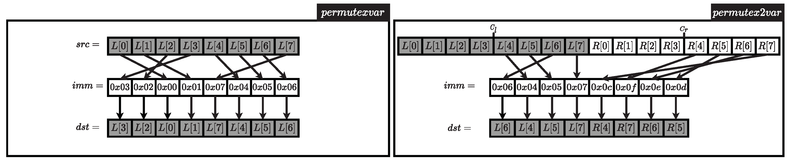
The Word Permutation () process involves rearranging the order of the hash digest in 64-bit units. While the permutation process for an LSH-512 implementation using 64-bit registers can be accomplished with a straightforward memory swap, challenges arise when dealing with registers longer than 64 bits, such as AVX. In the context of the LSH-512 process, AVX-512 registers containing hash digests need to reorder data across 64-bit boundaries. However, the process of converting AVX-512 registers to registers with different bit boundaries incurs a significant clock cost. Among the instructions that convert data to AVX-512 registers, has a latency of 8 and a throughput (CPI) of 0.5, while has a latency of 5 and a throughput (CPI) of 1 [56]. In other words, it requires a minimum latency of 13 to execute process. Consequently, we employed an instruction to substitute values within AVX-512 registers for handling process.
In our LSH-512 implementation, we update two registers, and , respectively, using two AVX-512 instructions to handle the LSH-512 permutation operation. Figure 2 provides a summary of these two permute instructions. The instruction shown in Figure 2 is designed to internally shuffle 512-bit registers in 64-bit units.Conversely, the instruction, also depicted in Figure 2, utilizes two 512-bit registers. This instruction allocates two registers in 64-bit units to the 512-bit registers. When storing a value in the data, the argument is employed to read data of the desired region from the two registers. Each of these instructions is utilized within the internal compression process. Both and are involved in updating . Therefore, our LSH implementation utilizes the instruction to handle the process. extracts the desired information from the two registers, and the extracted data are then stored in one register. This process is described in Figure 2. Algorithm 5 presents the pseudo-code for the process, where represents the permutation value. The process utilizes the permutation results outlined in Table 3. Consequently, the permutation values specified in Table 3 are assigned to .
| Algorithm 5 LSH-512 process using AVX-512 instructions |
| Require: , Ensure:
|
4.3. Proposed Implementation Clock Cost Analysis
Table 5 provides a summary of the clock cost generated by AVX-512 instructions. In our implementation of the process, we utilize two AVX-512 modular addition instructions and one AVX-512 permutexvar instruction. As a result, in our process, the clock cost is 5 latency and 2 throughput (CPI). Similarly, in our process implementation, we use three AVX-512 modular addition instructions, two bit-rotation instructions, one XOR instruction, and one shuffle instruction. The clock cost of the process is 7 latency and 5 throughput (CPI). For our implementation, we employ two permutex2var instructions, incurring a clock cost of 6 latency and 2 throughput (CPI).
The and instructions utilize permutation values. Therefore, the permutation values specified in Table 2 and Table 3 should be assigned to AVX-512 registers. However, assigning permutation values in each round function leads to frequent calls of the instruction, causing performance degradation. In our LSH-512 implementation, we optimize this process by initially assigning permutation values to AVX-512 registers and recycling them throughout the computation. By doing so, we eliminate frequent instruction calls, resulting in a clock cost of 24 + (19 × ) latency and 1.5 + (9.5 × ) throughput (CPI) in our LSH-512 compression function implementation.
5. Proposed Implementation Methods of LSH in GPU
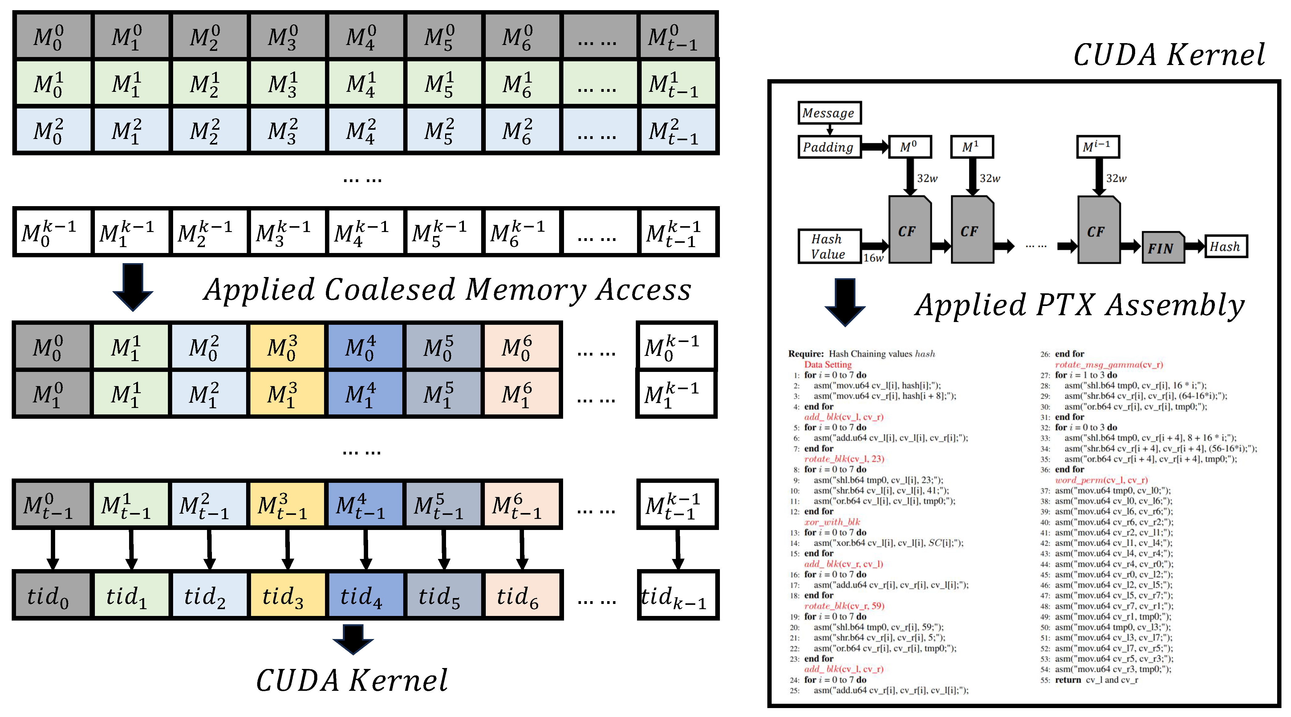
In this section, we present a parallel implementation of LSH-512 using CUDA. Our CUDA-based LSH-512 implementation is structured with data parallelism as the focus. Our approach involves leveraging CUDA streams and adopting a coalesced memory access pattern to minimize the performance overhead associated with global memory access, storage, and load operations in CUDA. Additionally, we introduce an implementation method for LSH-512 using Parallel Thread Execution (PTX) inline assembly. To the best of our knowledge, our study is the first attempt to implement LSH-512 based on a GPU. Our CUDA-based LSH-512 implementation is designed for data parallelism, with each thread handling LSH-512 operations on a single message. Figure 3 provides an overview of our parallel implementation scheme on a GPU architecture.
5.1. Coalesced Memory Access Methods
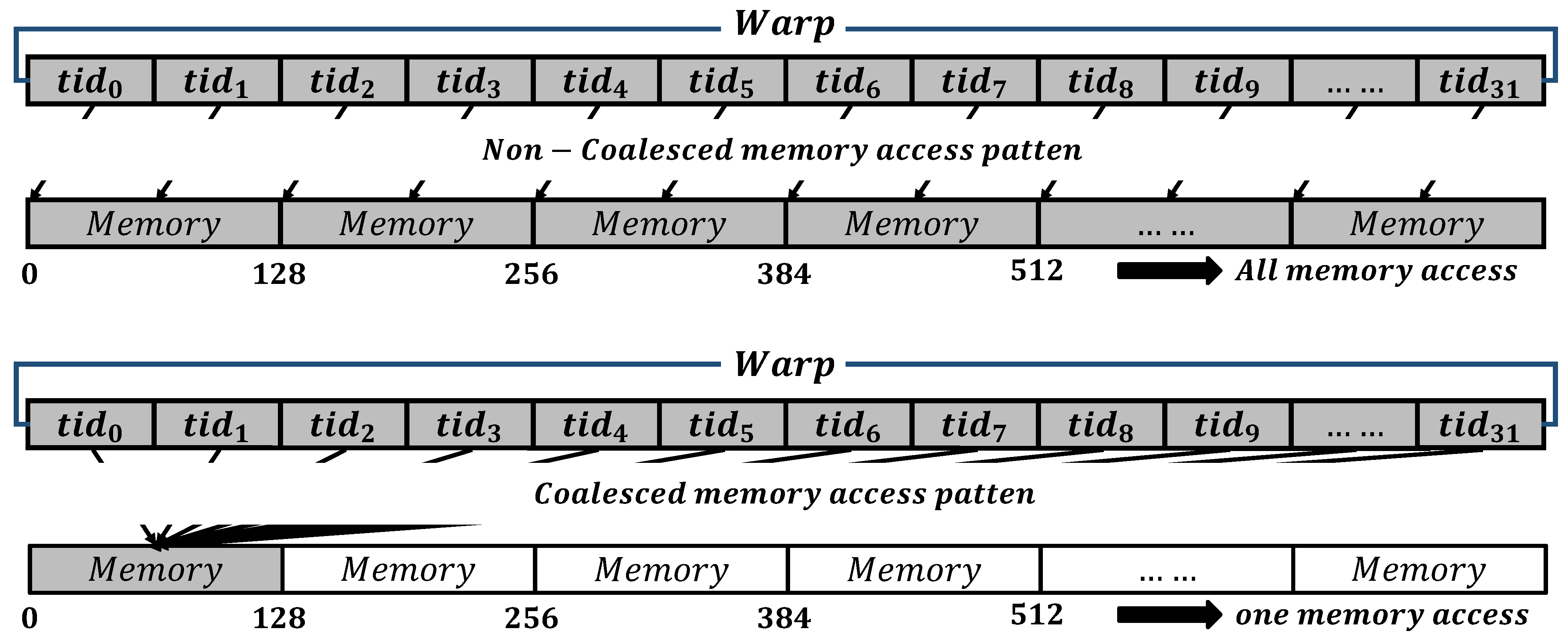
Figure 4 illustrates the comparison between coalesced and non-coalesced memory access. In NVIDIA GPUs, instructions are executed in units of 32 threads, referred to as a warp. Consequently, each thread within the same warp executes the same instruction. Coalesced memory access is an optimization technique applied to memory access within a warp. In this approach, when each thread within a warp handles memory access, the warp collectively accesses contiguous memory addresses [57]. In such cases, memory requests are efficiently. It is particularly effective in accessing the shared memory and global memory areas. However, if the memory addresses accessed by the warp are non-contiguous, the warp needs to access more memory. This results in frequent memory access and subsequent performance degradation. Therefore, our implementation adopts a coalesced memory access pattern to minimize the number of memory accesses within a warp.
Our LSH-512 implementation employs data parallelization, where each thread performs LSH-512 operations on an individual message. The process in our CUDA-based implementation is as follows. First, the CPU (Host) sends messages to the GPU (Device). Next, each thread loads a single message. Subsequently, each thread executes an LSH-512 hash on the message. Finally, the resulting hash values are sent from the GPU (Device) to the CPU (Host). In the second process, inefficient memory access can occur when each thread loads messages. Therefore, a message storage structure is implemented to facilitate coalesced memory access, while a common storage method for multiple messages is to organize them row by row, this leads to discontinuous memory addresses when warp threads access messages, resulting in frequent warp memory access. To minimize this, our LSH-512 implementation adopts a column-wise input message structure. If the storage structure of the input messages is initially organized in row units, the CPU adjusts the storage structure to column units. As a result, our LSH-512 implementation using CUDA modifies the storage structure of the input message column-by-column. The column-by-column storage minimizes memory access by arranging memory addresses accessed by warp threads consecutively. Additionally, in the final process, each thread stores the hash value in a dedicated memory area, enabling coalesced memory access during hash value storage. Algorithm 6 provides pseudo-code illustrating the coalesced memory access pattern in the input message and hash value storage process.
| Algorithm 6 LSH-512 coalesced memory access |
| Require: Input Message Ensure: LSH-512 Hash value
|
5.2. Cuda Stream
A CUDA stream is a concurrent process that performs operations on a device in the order specified by the CPU (Host) code. In essence, a CUDA stream is an object for asynchronous implementation in CUDA, allowing a single process to be divided into multiple processes. Up to 32 streams can be utilized in CUDA. Figure 5 provides an overview of CUDA streams, demonstrating their capability to run concurrently with other streams. As depicted in Figure 5, CUDA streams are applicable to tasks such as data transmission and kernel functions. In a CUDA process utilizing a single stream, data are transmitted from the CPU to the GPU for processing (referred to as the process). Basically, the memory transfer between the GPU and CPU is performed through the cudaMemcpy function. This is a synchronous data transfer function. In other words, if the cudaMemcpy function is used, the memory copy does not start until all previously existing CUDA calls have completed, and subsequent CUDA calls cannot begin until the synchronous transfer has completed. Therefore, if the data are large, a lot of latency occurs during data transfer from the CPU to the GPU. Likewise, data transfer from the GPU to the CPU incurs substantial latency. In the context of CUDA kernel operations, the processing time of the kernel increases proportionally with the number of tasks. CUDA streams facilitate simultaneous data transfer and kernel function processing. Figure 5 illustrates the transmission process of -byte data and the structure for processing four tasks using CUDA. In a scenario employing four streams, each stream incurs a n-byte data transfer time and one task processing kernel operation time. Consequently, task processing with multiple streams proves more efficient than a single-stream process. Therefore, our LSH-512 implementation adopts multiple CUDA streams to mitigate data transfer time and hash function kernel operation time.
5.3. Ptx Inline Assembly
PTX defines a virtual machine and Instruction Set Architecture (ISA) for general parallel thread execution [58]. Simply put, PTX offers an ISA that is independent of the specific NVIDIA GPU architecture [58]. In comparing CUDA C with PTX, it is crucial to note that PTX operates at a lower-level assembly language, providing developers with greater flexibility to optimize for distinct GPU architectures. Several reasons influenced our choice of PTX:
Architecture-specific optimizations: PTX code, being independent of a particular GPU architecture and serving as an intermediate assembly, boasts high portability. This characteristic enables the NVIDIA compiler to translate PTX code into machine language optimized for the specific nuances of different GPU architectures. Consequently, PTX facilitates the generation of optimized code that performs well across various GPU architectures;
Give developers granular control: PTX, being a lower-level assembly, unveils intricate details of the GPU architecture to developers. This exposure empowers developers to fine-tune their code, providing advanced control over specific hardware characteristics [36];
Optimized code generation: PTX serves as an intermediate assembly level, eventually translated into machine language optimized for a specific GPU architecture. This multi-step optimization process leads to improved performance [36].
In other words, PTX serves as a form of CUDA assembly, facilitating the conversion of high-level computing language to machine code during the compilation process of CUDA code, including nvcc. In CUDA, high-level language-based code, such as C/C++, undergoes compilation to generate PTX instructions. Throughout this conversion process, the PTX-based algorithm code has the capability to exclude unnecessary instructions generated during compilation. Consequently, our LSH-512 implementation is constructed based on PTX instructions. The PTX inline assembly instructions employed in our LSH-512 implementation are detailed in Table 6. LSH-512 operates with 64-bit words and follows an ARX structure internally. As a result, our LSH-512 implementation using PTX utilizes a 64-bit unit instruction type. The PTX inline assembly addition (add) instruction ensures that d = x + y mod . The pseudo-code outlining our LSH-512 process through PTX instructions is provided in Algorithm 7. In Algorithm 7, represents the round constant of LSH-512. With a focus on minimizing memory accesses on the GPU architecture, our LSH-512 implementation directly assigns the value of , avoiding the need for additional memory storage.
| Algorithm 7 LSH-512 function implementation method using PTX inline assembly |
 |
6. Performance Analysis
In this section, we present the performance measurements of LSH-512 and compare our implementation’s performance with other implementations. For our experimental measurements, we used an Intel Core i9-11900K (Rocket Lake) CPU, which supports both AVX-2 and AVX-512 instructions. In the case of our CPU environment experiments, we conducted the experiments using a single thread. In our experiments, the implementations used are our own work, KISA [42,59], and the work of Kim et al. [19]. We used Windows 10 OS and the IDE was Visual studio 2019 version. Our compilation options used Release Mode (x 64, - 03 option). Our AVX-512 performance measurement experiments present average values of 100,000 LSH-512 hash function operation clocks.
Additionally, for our GPU environment experiments, we utilized NVIDIA GeForce 2080ti and NVIDIA GeForce 3090 architectures. The NVIDIA GeForce 3090 architecture features 10,496 CUDA cores, employs a GA102 graphics processor, offers a bandwidth of 936.2 GB/s, and operates at a base clock of 1395 MHz. It boasts a compute capability of 8.6 and consumes 350 W of power. Conversely, the NVIDIA GeForce 2080ti architecture incorporates 4352 CUDA cores, utilizes the TU102 graphics processor, provides a bandwidth of 616.0 GB/s, and runs at a base clock of 1350 MHz. It has a compute capability of 7.5 and requires 250 W of power. For our GPU architecture experiments, we operated on the Windows 10 OS and utilized Visual Studio 2019 as the IDE. CUDA runtime version 10.2 served as the compiler, and we employed Release (x64, -O3 option) mode. Our GPU architecture experiments measured memory copy time and kernel function operation time, and the performance table presents the average time for 100 operations.
When designing GPGPU technology using CUDA, parallel computing units are divided into blocks and threads. In theory, calling the kernel with the maximum number of CUDA blocks and CUDA threads can maximize parallel processing of tasks. However, this is not possible due to GPU hardware. This is because there is a limit to the GPU resources actually used when the CUDA kernel is executed. The configuration that reaches the resource usage peak will vary depending on GPU architecture and workload. As a result, we analyze the performance threshold of our LSH-512 kernel through experiments on GPU architecture.
6.1. LSH-512 Performance Measurement Evaluation Using AVX-512
Our implementation is LSH-512 utilizing AVX-512. The reference implementation KISA [KISA] is an AVX-2 based LSH-512 reference implementation provided by the Korea Internet & Security Agency [42,59]. In addition, our implementation presents comparison results with that of Kim et al. [19]. We measured the performance of three codes in our CPU device environment. Table 7 contains our performance measurements.
Our LSH-512 implementation demonstrates performance improvements of 50.37% (LSH-512/224), 45.45% (LSH-512/256), 46.01% (LSH-512/384), and 45.74 (LSH-512/512)% for single-block processing compared to the existing AVX-2-based KISA standard reference code [42,59]. Additionally, our LSH-512 implementation exhibits performance enhancements of 20.61% (LSH-512/224), 19.40% (LSH-512/256), 19.70% (LSH-512/384), and 20.61% (LSH-512/512) when handling long message blocks compared to the AVX-2-based KISA standard reference code [42,59].
Our LSH-512 implementation demonstrates performance improvments of 161.52% (LSH-512/224), 135.09% (LSH-512/256), 159.11% (LSH-512/384), and 56.98% (LSH-512/512) for single-block processing compared to the AVX-2-based Kim et al. implementations [19]. Furthermore, our LSH-512 implementation achieves a remarkable performance improvement of 20.61% (LSH-512/224), 19.40% (LSH-512/256), 19.70% (LSH-512/384), and 20.61% for 16 MB message processing compared to Kim et al.’s AVX-2-based LSH implementation [19].
6.2. LSH-512/512 Performance Measurement Evaluation Using CUDA
Table 8 and Figure 6 present the results of CUDA stream performance measurements for LSH-512/512. The performance test fixes the CUDA blocks and threads to 4096 and 128, respectively. In this experiment, the number of CUDA streams gradually increases. [Opt.] denotes a version with our proposed LSH-512/512 optimization method applied. In the RTX 3090 architecture and RTX 2080ti architecture environments, CUDA stream performance test measurements show that performance increases with the growing number of CUDA streams. Consequently, our LSH-512/512 implementation achieves maximum performance when using 32 CUDA streams.
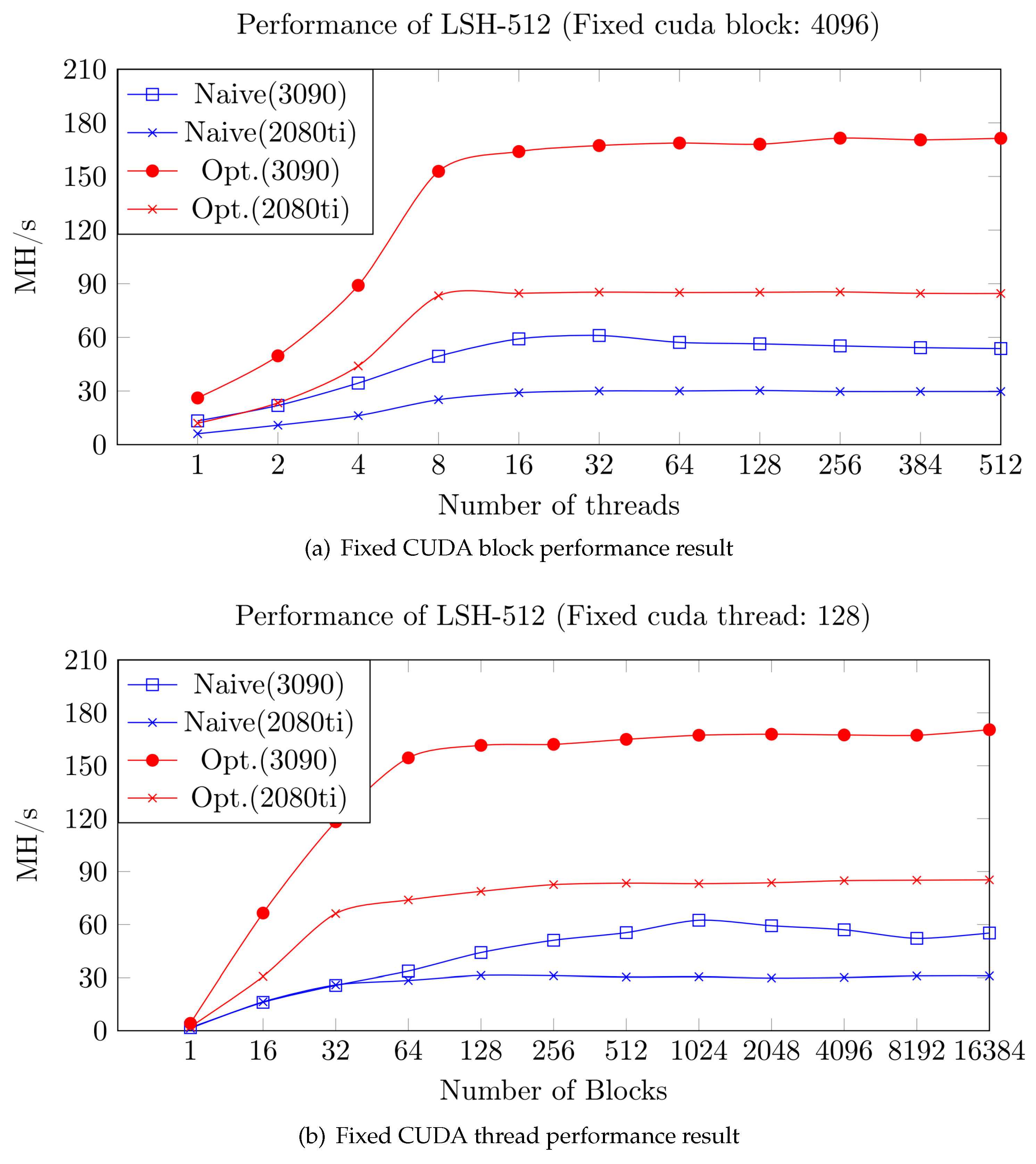
Figure 7 presents the performance results with a fixed number of CUDA blocks/threads. Specifically, Figure 7a and Table 9 display the performance measurements with a fixed number of CUDA blocks, set to 4096, while varying the number of threads. Similarly, Figure 7b and Table 10 show the performance measurements with a fixed number of CUDA threads, set to 128, while changing the number of blocks. The experimental unit is the number of LSH-512/512 operations per second. The [Naive] version benchmarks the KISA LSH-512/512 open-source code with CUDA C [42,59]. [Opt.] represents our LSH-512/512 optimization and parallelization method proposed in this paper. Both experimental results in Figure 7a,b fully utilize the resources of the GPU architecture, achieving maximum performance consistently by maximizing the use of the CUDA resources. In our fixed CUDA block experiments (Figure 7a) with the RTX 3090 architecture (resp. RTX 2080ti), our LSH-512/512 performance approaches up to 170 MH/s (resp. 85 MH/s). The LSH-512/512 benchmark’s performance approaches up to 60 MH/s. Similarly, in fixed CUDA threads LSH-512/512 performance experiments, our implementation on RTX 3090 (resp. RTX 2080ti) reaches a performance of 170 MH/s (resp. 85 MH/s). Table 9 and Table 10 present the performance measurement results of our LSH-512/512 implementation (Opt.) and benchmarking against the KISA open-source code (Naive). On the RTX 3090 (resp. RTX 2080ti) architecture, our LSH-512/512 implementation achieves up to 171.35 MH/s (resp. 85.41 MH/s), while the KISA open-source benchmarking code attains up to 61.06 MH/s (resp. 31.26 MH/s). Comparatively, on the RTX 3090 (resp. RTX 2080ti) architecture, our implementation demonstrates a significant performance improvement of 180.62% (resp. 173.22%) over the Naive version.
7. Discussion
In this paper, we introduced a parallel implementation technique for LSH-512 utilizing AVX-512. The register length difference between AVX-512 and AVX-256 is twice that of 256-bit and 512-bit, suggesting a potential 100% performance improvement proportional to the register length difference. However, our observed performance improvement rate is up to 50.37%. It is important to note that the rate of performance improvement gradually decreases. Our analysis suggests a bottleneck at the input message copy point. In future work, we aim to explore solutions to address the bottleneck related to the copying of input messages.
8. Conclusions
In this paper, we introduced parallel implementations of LSH-512 using SIMD AVX-512 instructions and CUDA. Additionally, we proposed an efficient AVX-512 implementation scheme for LSH-512 based on an in-depth analysis of AVX-512 instructions. Our AVX-512 implementation achieved a performance of 1.31 CPB, demonstrating a noteworthy improvement of up to 50.37% compared to other AVX-2 implementations. For our LSH-512 implementation using NVIDIA CUDA, we addressed the memory task bottleneck in GPU architecture. We proposed a coalesced memory access pattern, an effective memory access method, and an asynchronous parallel processing CUDA stream application. Furthermore, our LSH-512 implementation incorporates CUDA inline assembly PTX. On the RTX 3090 architecture, our implementation achieved a performance of up to 171.35 MH/s. To the best of our knowledge, our research represents the first optimization of LSH-512 on GPUs and AVX-512. In future work, we plan to explore optimization methods for hash-based high-level algorithms, including hash-based digital signature methods, message authentication codes, and password-based key derivation functions using LSH.
Author Contributions
H.C. and S.C.: Writing—original draft; S.S.: Writing—review and editing. All authors have read and agreed to the published version of the manuscript.
Funding
This work was partly supported by the National Research Foundataion of Korea (NRF) grant funded by the Korea government (MSIT) (No. 2022R1C1C1013368, 50%) and was partly supported by the Institute of Information and communications Technology Planning and Evaluation (IITP) Grant by the Korean Government through Ministry of Science and ICT (MSIT) (A study on PQC optimization and security protocol migration to neutralize advanced quantum attacks in Beyond 5G-based next-generation IoT computing environments, 50%) under Grant 2022-00207416.
Data Availability Statement
Data are contained within the article.
Acknowledgments
We would like to express our gratitude to the anonymous reviewers who provided valuable comments.
Conflicts of Interest
The authors declare no conflicts of interest.
References
- Turner, J.M. The keyed-hash message authentication code (HMAC). Fed. Inf. Process. Stand. Publ. 2008, 198, 1–13. [Google Scholar]
- Kaliski, B. PKCS# 5: Password-Based Cryptography Specification Version 2.0; Technical Report; The Internet Society: Reston, VI, USA, 2000. [Google Scholar]
- Barker, E.B.; Kelsey, J.M. Recommendation for Random Number Generation Using Deterministic Random Bit Generators (Revised); US Department of Commerce, Technology Administration, National Institute of Standrads and Technology: Gaithersburg, MD, USA, 2007. [Google Scholar]
- Kerry, C.F.; Gallagher, P.D. FIPS PUB 186-2; Digital Signature Standard (DSS). Federal Information Processing Standards Publications: Gaithersburg, MD, USA, 2013; pp. 186–194.
- Ducas, L.; Kiltz, E.; Lepoint, T.; Lyubashevsky, V.; Schwabe, P.; Seiler, G.; Stehlé, D. CRYSTALS-DILITHIUM—Submission to Round 3 of NIST’s Post-Quantum Cryptography Standardization Process; Rep.(NISTIR)-8413; National Institute of Standards and Technology (NIST): Gaithersburg, MD, USA, 2020. [Google Scholar]
- Fouque, P.A.; Hoffstein, J.; Kirchner, P.; Lyubashevsky, V.; Pornin, T.; Prest, T.; Ricosset, T.; Seiler, G.; Whyte, W.; Zhang, Z. Falcon: Fast-Fourier Lattice-Based Compact Signatures over NTRU. Submiss. NIST Post-Quantum Cryptogr. Stand. Process 2018, 36, 1–75. [Google Scholar]
- Avanzi, R.; Bos, J.; Ducas, L.; Kiltz, E.; Lepoint, T.; Lyubashevsky, V.; Schanck, J.M.; Schwabe, P.; Seiler, G.; Stehlé, D. CRYSTALS Kyber. Submission to the NIST Post-Quantum Cryptography Standardization Project; NIST National Institute of Standards and Technology: Gaithersburg, MD, USA, 2020. [Google Scholar]
- Lamport, L. Constructing Digital Signatures from a One Way Function; 1979. Available online: https://www.microsoft.com/en-us/research/publication/constructing-digital-signatures-one-way-function/ (accessed on 30 October 2023).
- Buchmann, J.; Dahmen, E.; Ereth, S.; Hülsing, A.; Rückert, M. On the security of the Winternitz one-time signature scheme. Int. J. Appl. Cryptogr. 2013, 3, 84–96. [Google Scholar] [CrossRef]
- Merkle, R.C. A Certified Digital Signature. In Advances in Cryptology—CRYPTO ’89, 9th Annual International Cryptology Conference, Santa Barbara, CA, USA, 20–24 August 1989, Proceedings; Brassard, G., Ed.; Lecture Notes in Computer Science; Springer: New York, NY, USA, 1989; Volume 435, pp. 218–238. [Google Scholar] [CrossRef]
- Bernstein, D.J.; Hopwood, D.; Hülsing, A.; Lange, T.; Niederhagen, R.; Papachristodoulou, L.; Schneider, M.; Schwabe, P.; Wilcox-O’Hearn, Z. SPHINCS: Practical Stateless Hash-Based Signatures. In Advances in Cryptology—EUROCRYPT 2015—34th Annual International Conference on the Theory and Applications of Cryptographic Techniques, Sofia, Bulgaria, 26–30 April 2015, Proceedings; Part I; Oswald, E., Fischlin, M., Eds.; Lecture Notes in Computer Science; Springer: Berlin/Heidelberg, Germany, 2015; Volume 9056, pp. 368–397. [Google Scholar] [CrossRef]
- Bernstein, D.J.; Hülsing, A.; Kölbl, S.; Niederhagen, R.; Rijneveld, J.; Schwabe, P. The SPHINCS+ Signature Framework. In Proceedings of the CCS ’19: 2019 ACM SIGSAC Conference on Computer and Communications Security, London, UK, 11–15 November 2019; Cavallaro, L., Kinder, J., Wang, X., Katz, J., Eds.; ACM: New York, NY, USA, 2019; pp. 2129–2146. [Google Scholar] [CrossRef]
- Kim, D.C.; Hong, D.; Lee, J.K.; Kim, W.H.; Kwon, D. LSH: A new fast secure hash function family. In Information Security and Cryptology-ICISC 2014: 17th International Conference, Seoul, Republic of Korea, 3–5 December 2014; Revised Selected Papers 17; Springer: Berlin/Heidelberg, Germany, 2015; pp. 286–313. [Google Scholar]
- ISO/IEC 19790:2012; Information Technology—Security Techniques Security Requirements for Cryptographic Modules. Korea Standards Association: Seoul, Republic of Korea, 2012.
- Sim, M.; Eum, S.; Song, G.; Kwon, H.; Jang, K.; Kim, H.; Kim, H.; Yang, Y.; Kim, W.; Lee, W.K.; et al. K-XMSS and K-SPHINCS+: Hash based Signatures with Korean Cryptography Algorithms. Cryptol. Eprint Arch. 2022. [Google Scholar]
- NVIDIA. CUDA C++ Programming Guide. 2024. Available online: https://docs.nvidia.com/cuda/cuda-c-programming-guide/index.html (accessed on 8 January 2024).
- Owens, J.D.; Houston, M.; Luebke, D.; Green, S.; Stone, J.E.; Phillips, J.C. GPU computing. Proc. IEEE 2008, 96, 879–899. [Google Scholar] [CrossRef]
- Keckler, S.W.; Dally, W.J.; Khailany, B.; Garland, M.; Glasco, D. GPUs and the future of parallel computing. IEEE Micro 2011, 31, 7–17. [Google Scholar] [CrossRef]
- Kim, D.; Jung, Y.; Ju, Y.; Song, J. Fast implementation of LSH with SIMD. IEEE Access 2019, 7, 107016–107024. [Google Scholar] [CrossRef]
- Park, T.; Seo, H.; Kim, H. Fast implementation of simeck family block ciphers using avx2. In Proceedings of the 2018 International Conference on Platform Technology and Service (PlatCon), Jeju, Republic of Korea, 29–31 January 2018; pp. 1–6. [Google Scholar]
- Cabral, R.; López, J. Implementation of the SHA-3 family using AVX512 instructions. In Proceedings of the Anais do XVIII Simpósio Brasileiro de Segurança da Informação e de Sistemas Computacionais. SBC, Natal, Brazil, 25 October 2018; pp. 25–32. [Google Scholar]
- Cheng, H.; Großschädl, J.; Tian, J.; Rønne, P.B.; Ryan, P.Y. High-throughput elliptic curve cryptography using AVX2 vector instructions. In Selected Areas in Cryptography: 27th International Conference, Halifax, NS, Canada, 21–23 October 2020; Revised Selected Papers 27; Springer: Cham, Switzerland, 2021; pp. 698–719. [Google Scholar]
- Alter, D.M.; Schwabe, P.; Daemen, J. Optimizing the NIST Post Quantum Candidate SPHINCS+ Using AVX-512. 2021. Available online: https://www.cs.ru.nl/bachelors-theses/2021/Dor_Mariel_Alter___1027021 (accessed on 25 August 2021).
- Duong-Ngoc, P.; Tan, T.N.; Lee, H. Efficient NewHope cryptography based facial security system on a GPU. IEEE Access 2020, 8, 108158–108168. [Google Scholar] [CrossRef]
- Lee, W.K.; Seo, H.; Zhang, Z.; Hwang, S.O. Tensorcrypto: High throughput acceleration of lattice-based cryptography using tensor core on gpu. IEEE Access 2022, 10, 20616–20632. [Google Scholar] [CrossRef]
- Lee, K.; Gowanlock, M.; Cambou, B. SABER-GPU: A Response-Based Cryptography Algorithm for SABER on the GPU. In Proceedings of the 2021 IEEE 26th Pacific Rim International Symposium on Dependable Computing (PRDC), Perth, Australia, 1–4 December 2021; pp. 123–132. [Google Scholar]
- Gupta, N.; Jati, A.; Chauhan, A.K.; Chattopadhyay, A. Pqc acceleration using gpus: Frodokem, newhope, and kyber. IEEE Trans. Parallel Distrib. Syst. 2020, 32, 575–586. [Google Scholar] [CrossRef]
- Seo, S.C. SIKE on GPU: Accelerating supersingular isogeny-based key encapsulation mechanism on graphic processing units. IEEE Access 2021, 9, 116731–116744. [Google Scholar] [CrossRef]
- An, S.; Seo, S.C. Efficient parallel implementations of LWE-based post-quantum cryptosystems on graphics processing units. Mathematics 2020, 8, 1781. [Google Scholar] [CrossRef]
- Ji, X.; Dong, J.; Zhang, P.; Tonggui, D.; Jiafeng, H.; Xiao, F. HI-Kyber: A Novel High-Performance Implementation Scheme of Kyber Based on GPU. Cryptology ePrint Archive, Paper 2023/1194. 2023. Available online: https://eprint.iacr.org/2023/1194 (accessed on 7 August 2023).
- Pan, W.; Zheng, F.; Zhao, Y.; Zhu, W.T.; Jing, J. An efficient elliptic curve cryptography signature server with GPU acceleration. IEEE Trans. Inf. Forensics Secur. 2016, 12, 111–122. [Google Scholar] [CrossRef]
- Dong, J.; Zheng, F.; Lin, J.; Liu, Z.; Xiao, F.; Fan, G. EC-ECC: Accelerating elliptic curve cryptography for edge computing on embedded GPU TX2. ACM Trans. Embed. Comput. Syst. (TECS) 2022, 21, 1–25. [Google Scholar] [CrossRef]
- Gao, L.; Zheng, F.; Emmart, N.; Dong, J.; Lin, J.; Weems, C. DPF-ECC: Accelerating elliptic curve cryptography with floating-point computing power of gpus. In Proceedings of the 2020 IEEE International Parallel and Distributed Processing Symposium (IPDPS), New Orleans, LA, USA, 18–22 May 2020; pp. 494–504. [Google Scholar]
- Chugh, G.; Saji, S.A.; Singh Bhati, N. Fast Implementation of AES Modes Based on Turing Architecture. In Advancements in Interdisciplinary Research: First International Conference, AIR 2022, Prayagraj, India, 6–7 May 2022; Revised Selected Papers; Springer: Cham, Switzerland, 2023; pp. 479–489. [Google Scholar]
- An, S.; Seo, S.C. Designing a new XTS-AES parallel optimization implementation technique for fast file encryption. IEEE Access 2022, 10, 25349–25357. [Google Scholar] [CrossRef]
- An, S.; Seo, S.C. Highly Efficient Implementation of Block Ciphers on Graphic Processing Units for Massively Large Data. Appl. Sci. 2020, 10, 3711. [Google Scholar] [CrossRef]
- Choi, H.; Seo, S.C. Fast implementation of SHA-3 in GPU environment. IEEE Access 2021, 9, 144574–144586. [Google Scholar] [CrossRef]
- Wang, C.; Chu, X. GPU accelerated Keccak (SHA3) algorithm. arXiv 2019, arXiv:1902.05320. [Google Scholar]
- Dat, T.N.; Iwai, K.; Matsubara, T.; Kurokawa, T. Implementation of high speed hash function Keccak on GPU. Int. J. Netw. Comput. 2019, 9, 370–389. [Google Scholar] [CrossRef]
- Kuznetsov, A.; Shekhanin, K.; Kolhatin, A.; Kovalchuk, D.; Babenko, V.; Perevozova, I. Performance of Hash Algorithms on Gpus for Use in Blockchain. In Proceedings of the 2019 IEEE international conference on advanced trends in information theory (ATIT), Kyiv, Ukraine, 18–20 December 2019; pp. 166–170. [Google Scholar]
- Iuorio, A.F.; Visconti, A. Understanding optimizations and measuring performances of PBKDF2. In 2nd International Conference on Wireless Intelligent and Distributed Environment for Communication: WIDECOM 2019; Springer: Cham, Switzerland, 2019; pp. 101–114. [Google Scholar]
- Kisa, K. Lightweight Secure Hash Function Open Source Code. 2023. Available online: https://seed.kisa.or.kr/kisa/Board/22/detailView.do (accessed on 31 January 2019).
- Kusswurm, D. Modern Parallel Programming with C++ and Assembly; Apress: Berkeley, CA, USA, 2022. [Google Scholar] [CrossRef]
- Verma, R.; Vishnu, V.; Kataoka, K. Verifiable and Robust Monitoring and Alerting System for Road Safety by AI based Consensus Development on Blockchain. In Proceedings of the 2023 IEEE Intelligent Vehicles Symposium (IV), Anchorage, AK, USA, 4–7 June 2023; pp. 1–8. [Google Scholar]
- Qureshi, R.; Irfan, M.; Ali, H.; Khan, A.; Nittala, A.S.; Ali, S.; Shah, A.; Gondal, T.M.; Sadak, F.; Shah, Z.; et al. Artificial Intelligence and Biosensors in Healthcare and its Clinical Relevance: A Review. IEEE Access 2023, 11, 61600–61620. [Google Scholar] [CrossRef]
- Seng, K.P.; Ang, L.M. Embedded intelligence: State-of-the-art and research challenges. IEEE Access 2022, 10, 59236–59258. [Google Scholar] [CrossRef]
- Kumar, M.; Kaur, G. Containerized AI Framework on Secure Shared Multi-GPU Systems. In Proceedings of the 2022 Seventh International Conference on Parallel, Distributed and Grid Computing (PDGC), Solan, Himachal Pradesh, India, 25–27 November 2022; pp. 243–247. [Google Scholar]
- Kumar, M.; Kaur, G. Study of container-based JupyterLab and AI Framework on HPC with GPU usage. In Proceedings of the 2022 International Conference on Smart Generation Computing, Communication and Networking (SMART GENCON), Bangalore, India, 23–25 December 2022; pp. 1–5. [Google Scholar]
- Li, H.; Ng, J.K.; Abdelzaher, T. Enabling Real-time AI Inference on Mobile Devices via GPU-CPU Collaborative Execution. In Proceedings of the 2022 IEEE 28th International Conference on Embedded and Real-Time Computing Systems and Applications (RTCSA), Taipei, Taiwan, 23–25 August 2022; pp. 195–204. [Google Scholar]
- Bataineh, M.R.; Mardini, W.; Khamayseh, Y.M.; Yassein, M.M.B. Novel and secure blockchain framework for health applications in IoT. IEEE Access 2022, 10, 14914–14926. [Google Scholar] [CrossRef]
- Pandya, S.B.; Sanghvi, H.A.; Patel, R.H.; Pandya, A.S. GPU and FPGA Based Deployment of Blockchain for Cryptocurrency—A Systematic Review. In Proceedings of the 2022 International Conference on Computational Intelligence and Sustainable Engineering Solutions (CISES), Greater Noida, India, 20–21 May 2022; pp. 18–25. [Google Scholar]
- Morishima, S.; Matsutani, H. Accelerating blockchain search of full nodes using GPUs. In Proceedings of the 2018 26th Euromicro International Conference on Parallel, Distributed and Network-based Processing (PDP), Cambridge, UK, 21–23 March 2018; pp. 244–248. [Google Scholar]
- Lessley, B.; Childs, H. Data-parallel hashing techniques for GPU architectures. IEEE Trans. Parallel Distrib. Syst. 2019, 31, 237–250. [Google Scholar] [CrossRef]
- CUDA NVIDIA. NVIDIA CUDA Compute Unified Device Architecture Programming Guide. 2007. Available online: https://developer.download.nvidia.com/compute/cuda/1.0/NVIDIA_CUDA_Programming_Guide_1.0.pdf (accessed on 30 October 2023).
- Munshi, A. The opencl specification. In Proceedings of the 2009 IEEE Hot Chips 21 Symposium (HCS), Stanford, CA, USA, 23–25 August 2009; pp. 1–314. [Google Scholar]
- Intel. Intel Advanced Vector Extensions 512 Instructions. 2017. Available online: https://www.intel.com/content/www/us/en/developer/articles/technical/intel-avx-512-instructions.html?wapkw=AVX-512 (accessed on 20 June 2017).
- NVIDIA. CUDA C++ Best Practices Guide. 2023. Available online: https://docs.nvidia.com/cuda/cuda-c-best-practices-guide/index.html (accessed on 14 November 2023).
- NVIDIA. CUDA Toolkit v12.0.1 PTX ISA. 2023. Available online: https://docs.nvidia.com/cuda/parallel-thread-execution/index.html (accessed on 14 November 2023).
- Lightweight Secure Hash Function Source Codes. 2023. Available online: https://github.com/sjnst217/KISA_LSH (accessed on 27 September 2023).
Figure 1.
LSH process.

Figure 2.
AVX-512 permutexvar and permutex2var instructions.

Figure 3.
Proposed implementation methods of LSH in a GPU.

Figure 4.
Non-Coalesced memory access pattern and coalesced memory access pattern.

Figure 5.
CUDA streams.

Figure 6.
LSH-512/512 CUDA stream performance analysis.

Figure 7.
LSH-512 performance results on GPU Architectures (Graph).


Table 1.
Notations.
| Symbol | Operation |
|---|---|
| X & Y | Bitwise AND operation of X and Y |
| X|Y | Bitwise OR operation of X and Y |
| X⊕Y | Bitwise XOR operation of X and Y |
| X⊞Y | Modular addition of X and Y in |
| X‖Y | Concatenation of X and Y |
| X≪n | n-bit center shift operation on X |
| X≫n | n-bit right shift operation on X |
| n-bit center rotation operation on X | |
| n-bit right rotation operation on X |
Table 2.
LSH Message Expansion value.
| I | 0 | 1 | 2 | 3 | 4 | 5 | 6 | 7 |
|---|---|---|---|---|---|---|---|---|
| 3 | 2 | 1 | 0 | 7 | 4 | 5 | 6 | |
| I | 8 | 9 | 10 | 11 | 12 | 13 | 14 | 15 |
| 11 | 10 | 8 | 9 | 15 | 12 | 13 | 14 |
Table 3.
LSH Word Permutation value.
| I | 0 | 1 | 2 | 3 | 4 | 5 | 6 | 7 |
|---|---|---|---|---|---|---|---|---|
| [I] | 6 | 4 | 5 | 7 | 12 | 15 | 14 | 13 |
| I | 8 | 9 | 10 | 11 | 12 | 13 | 14 | 15 |
| [I] | 2 | 0 | 1 | 3 | 8 | 11 | 10 | 9 |
Table 4.
AVX-512 instruction sets.
| Operation | Unit | AVX-512 Instruction |
|---|---|---|
| XOR | 32-bit | _mm512_xor_epi32(x, y) |
| 64-bit | _mm512_xor_epi64(x, y) | |
| 512-bit | _mm512_xor_si512(x, y) | |
| OR | 32-bit | _mm512_or_epi32(x, y) |
| 64-bit | _mm512_or_epi64(x, y) | |
| 512-bit | _mm512_or_si512(x, y) | |
| AND | 32-bit | _mm512_and_epi32(x, y) |
| 64-bit | _mm512_and_epi64(x, y) | |
| 512-bit | _mm512_and_si512(x, y) | |
| Left Shift | 32-bit | _mm512_slli_epi32(x, y) |
| 64-bit | _mm512_slli_epi64(x, y) | |
| Modular Addition | 16-bit | _mm512_add_epi16(x, y) |
| 32-bit | _mm512_add_epi32(x, y) | |
| 64-bit | _mm512_add_epi64(x, y) | |
| Rotation | 32-bit | _mm512_rol_epi32(x, imm) |
| 64-bit | _mm512_ror_epi64(x, imm) |
Table 5.
AVX-512 instruction costs [56].
Table 5.
AVX-512 instruction costs [56].
| Operation | Latency | Throughput (CPI) |
|---|---|---|
| 1 | 0.5 | |
| 1 | 0.5 | |
| 1 | 1 | |
| 1 | 1 | |
| 3 | 1 | |
| 3 | 1 | |
| 8 | 0.5 |
Table 6.
PTX inline assembly instruction using LSH-512 implementation [58].
Table 6.
PTX inline assembly instruction using LSH-512 implementation [58].
| PTX Instruction | LSH-512 Type | Operation |
|---|---|---|
| mov.type dst, src | u64 | dst = src |
| xor.type dst, src1, src2 | b64 | dst = src1 ⊕ src2 |
| or.type dst, src1, src2 | b64 | dst = src1 | src2 |
| shl.type, dst, src, imm | b64 | dst = src ≪ imm |
| shr.type, dst, src, imm | b64 | dst = src ≫ imm |
| add.type, dst, src1, src2 | u64 | dst = src1 + src2 |
Table 7.
LSH-512 performance measurement evaluation in CPU device (i9-11900k Rocket Lake).
| Function | Hash Digest (Bit) | SIMD | Version | Performance (CPB) | ||
|---|---|---|---|---|---|---|
| 16 MB | 4 KB | 64-Byte | ||||
| LSH- 512/224 | 224 | AVX-2 | KISA [42,59] | 1.58 | 1.75 | 8.09 |
| Kim et al. [19] | 1.62 | 1.81 | 14.07 | |||
| AVX_512 | Our Works | 1.31 | 1.42 | 5.38 | ||
| LSH- 512/256 | 256 | AVX-2 | KISA [42,59] | 1.60 | 1.74 | 8.00 |
| Kim et al. [19] | 1.60 | 1.73 | 12.93 | |||
| AVX_512 | Our Works | 1.34 | 1.42 | 5.50 | ||
| LSH- 512/384 | 384 | AVX-2 | KISA [42,59] | 1.58 | 1.76 | 8.25 |
| Kim et al. [19] | 1.59 | 1.86 | 14.64 | |||
| AVX_512 | Our Works | 1.32 | 1.41 | 5.65 | ||
| LSH- 512/512 | 512 | AVX-2 | KISA [42,59] | 1.58 | 1.75 | 8.03 |
| Kim et al. [19] | 1.56 | 1.65 | 8.65 | |||
| AVX_512 | Our Works | 1.31 | 1.42 | 5.51 | ||
Table 8.
LSH-512/512 CUDA stream performance analysis (Fixed CUDA blocks/threads: (4096/128).
| Device | Number of CUDA Streams | |||||
|---|---|---|---|---|---|---|
| 2 | 4 | 8 | 16 | 24 | 32 | |
| RTX 3090 | 131.49 | 149.73 | 159.18 | 163.65 | 164.89 | 167.44 |
| RTX 2080ti | 64.71 | 75.53 | 80.73 | 81.12 | 81.54 | 84.87 |
Table 9.
LSH-512/512 performance analysis on GPU Architecture (Fixed CUDA blocks: 4096, Unit: MH/s).
Table 9.
LSH-512/512 performance analysis on GPU Architecture (Fixed CUDA blocks: 4096, Unit: MH/s).
| Version | Number of CUDA Threads | ||||||||||
|---|---|---|---|---|---|---|---|---|---|---|---|
| 1 | 2 | 4 | 8 | 16 | 32 | 64 | 128 | 256 | 384 | 512 | |
| Naive (3090) | 13.30 | 21.90 | 34.43 | 49.44 | 59.17 | 61.06 | 57.20 | 56.39 | 55.25 | 54.25 | 53.75 |
| Naive (2080ti) | 6.11 | 10.87 | 16.23 | 25.14 | 29.05 | 30.04 | 30.04 | 30.28 | 29.72 | 29.74 | 29.72 |
| Opt. (3090) | 26.13 | 49.67 | 89.08 | 152.88 | 163.94 | 167.29 | 168.70 | 168.05 | 171.43 | 170.49 | 171.35 |
| Opt. (2080ti) | 12.02 | 23.35 | 44.02 | 83.27 | 84.65 | 85.30 | 85.08 | 85.21 | 85.41 | 84.61 | 84.55 |
Table 10.
LSH-512/512 performance analysis on GPU Architecture (Fixed CUDA threads: 128, Unit: MH/s).
Table 10.
LSH-512/512 performance analysis on GPU Architecture (Fixed CUDA threads: 128, Unit: MH/s).
| Version | Number of CUDA Blocks | |||||||||||
|---|---|---|---|---|---|---|---|---|---|---|---|---|
| 1 | 16 | 32 | 64 | 128 | 256 | 512 | 1024 | 2048 | 4096 | 8192 | 16,384 | |
| Naive (3090) | 1.73 | 16.08 | 25.64 | 33.69 | 44.14 | 51.09 | 55.42 | 62.43 | 59.31 | 57.02 | 52.17 | 55.20 |
| Naive (2080ti) | 1.37 | 16.36 | 25.92 | 28.41 | 31.26 | 31.08 | 30.33 | 30.49 | 29.77 | 30.09 | 30.96 | 30.98 |
| Opt. (3090) | 4.20 | 66.50 | 118.24 | 154.46 | 161.54 | 162.12 | 164.95 | 167.28 | 167.87 | 167.44 | 167.27 | 170.43 |
| Opt. (2080ti) | 2.20 | 30.70 | 66.20 | 73.93 | 78.79 | 82.61 | 83.45 | 83.16 | 83.68 | 84.87 | 85.14 | 85.30 |
Disclaimer/Publisher’s Note: The statements, opinions and data contained in all publications are solely those of the individual author(s) and contributor(s) and not of MDPI and/or the editor(s). MDPI and/or the editor(s) disclaim responsibility for any injury to people or property resulting from any ideas, methods, instructions or products referred to in the content. |
© 2024 by the authors. Licensee MDPI, Basel, Switzerland. This article is an open access article distributed under the terms and conditions of the Creative Commons Attribution (CC BY) license (https://creativecommons.org/licenses/by/4.0/).
Share and Cite
MDPI and ACS Style
Choi, H.; Choi, S.; Seo, S. Parallel Implementation of Lightweight Secure Hash Algorithm on CPU and GPU Environments. Electronics 2024, 13, 896. https://doi.org/10.3390/electronics13050896
AMA Style
Choi H, Choi S, Seo S. Parallel Implementation of Lightweight Secure Hash Algorithm on CPU and GPU Environments. Electronics. 2024; 13(5):896. https://doi.org/10.3390/electronics13050896
Chicago/Turabian StyleChoi, Hojin, SeongJun Choi, and SeogChung Seo. 2024. "Parallel Implementation of Lightweight Secure Hash Algorithm on CPU and GPU Environments" Electronics 13, no. 5: 896. https://doi.org/10.3390/electronics13050896
Note that from the first issue of 2016, this journal uses article numbers instead of page numbers. See further details here.