1. Introduction
Monolithic Microwave Integrated Circuits (MMICs) are key components for the deployment of the next generation of communication systems, e.g., 5G/6G mobile networks, where the main challenges are represented by the increasing operating frequency, higher efficiency, and power handling capability. Regardless of the technology adopted, either Silicon-based or III-V compound semiconductors, microwave and millimeter-wave active analog circuits ask for (1) reduced transistors’ gate lengths (100 nm or less) and (2) rather complex matching structures, typically designed according to a semi-lumped approach to achieve compact chips, which require full-wave electromagnetic (EM) simulation to accurately model coupling effects. These two features make Process Induced Variability (PIV) due to process uncertainties and tolerances a potential issue, for both the active devices, especially in case of less mature emerging high-power III-V technologies such as GaN, and passive networks, where even small fabrication tolerances can significantly impact the resonance frequency and losses of a filtering stage. This makes statistical or, more generally, PIV-aware microwave circuit design, a research field of growing interest [
1,
2,
3]. Hence, the development of models capable of including the inherent parameter variability in MMIC simulation, since the very first design steps, is of great interest. Such models should not only be highly accurate in predicting MMIC performance under linear and non-linear simulations, but also computationally efficient to allow for statistical and yield analysis, typically based on Monte Carlo (MC) simulations.
Technology CAD (TCAD)-based and EM statistical models provide the highest accuracy and retain the relationship with physical parameters of transistors and network elements [
4,
5], but they both are too computationally expensive to be directly exploited for MC analysis. For passive microwave circuits, several methods to avoid the computational effort of EM analysis have been proposed so far, such as space-mapping [
6], response surface approximation [
7], or polynomial chaos expansion [
8], but the embedding of such mathematical models into microwave CAD tools is not always straightforward. On the other hand, circuit equivalent models, which are typically provided within foundry process design kits (PDKs), allow for the statistics to be applied only to isolated elements, neglecting fundamental EM effects such as the effective current distribution along transmission lines, the cross-talk among adjacent structures, the end/edge effects, and the impact of the lumped elements’ aspect ratio on their behavior.
When power comes to play, as in power amplifiers (PAs) or mixers, the active device non-linear behavior must also be accurately reproduced. The statistical models available in literature (and in PDKs) are typically based on circuit equivalents [
1,
9,
10,
11]. However, in the active devices, the variation of one electrical characteristic is typically due to the concurrent effect of many different process variations, thus the adoption of a circuit statistical model, where the direct connection between the process fluctuation and circuit performance variation is lost, hinders the possibility to distinguish between high- and low-sensitivity technological parameters.
In Ref. [
12] we demonstrated that black-box models are the ideal framework for the implementation of physics-based yet numerically efficient statistical models, extremely easy to be included into CAD tools. As detailed in Ref. [
13], for the active device, an effective choice—at least in narrowband operation—is the X-parameter model, based on the poly-harmonic description of a non-linear device [
14]. In a similar fashion, the passive EM-simulated networks can be efficiently represented by parameterized S-parameter blocks [
15].
In this paper, which follows up from Ref. [
12], we apply the proposed behavioral models (parameterized X-parameters and S-parameters) to the statistical analysis of microwave PAs, aimed at providing the spread of the final PA performance directly from multiple, possibly correlated, statistical variations in the technology, and at identifying the parameters characterized by the largest sensitivity. We address, in particular, the design of a single-stage and of a combined X-band PA at 12 GHz based on a 1 mm GaAs device undergoing uniform doping variations in the active device channel. Concurrently, we analyze the effect of PIV in passive networks, focusing on the main source of variability, i.e., the thickness of the dielectric layer used for the fabrication of the MIM capacitors adopted for matching and power combination. The behavioral models are efficiently identified directly from a limited set of accurate physics-based analyses vs. selected technological parameters, both for the active and passive blocks, and then implemented into a CAD tool for fast and efficient MMIC-level statistical analysis, retaining a direct link to the underlying process. Even with only two physical parameters considered, the performance spread is significant, confirming the paramount importance of statistical analysis in MMIC design optimization.
The organization of the paper is as follows: in
Section 2 we briefly review the modeling approach, while in
Section 3 and
Section 4 we address the single and combined PA statistical analysis, respectively.
2. Behavioral Models
As detailed in Ref. [
12], the modeling approach consists in partitioning the microwave circuit in a block-wise fashion, as shown in
Figure 1, where each block represents a physical section of the circuit. The distinctive feature of each block is whether it requires a linear or a nonlinear model to be described: hence the partition encompasses one (or a set of) fully linear block(s) (
Figure 1, left), including matching, stabilization, biasing and coupling networks, and one (or several) nonlinear block(s) including the active device(s) (
Figure 1, center). The final circuit behavior is obtained by linking the various blocks through a set of
interconnecting ports (
Figure 1, right). Notice that for microwave circuits, port waves [
16] are the most natural port variables and have thus been preferred with respect to port voltages or currents.
Figure 1 also highlights the behavioral model extraction flow. Each block is first described considering its physical structure (
Figure 1, top), including all the geometrical and material properties of the specific fabrication technology adopted. Then the blocks are analyzed, adopting physics-based simulators (
Figure 1, middle), namely an EM solver for the passive networks (planar-3D solvers can be used in case of microstrip structures to speed up simulations) and a TCAD tool for the active devices. Finally (
Figure 1, bottom), the results of the physics-based analysis are used to extract the
behavioral (black-box) models, describing the blocks in terms of incident and reflected port waves. The models are parameterized with respect to one or more selected technological parameters. As detailed in Ref. [
12], both the linearized and incremental approach can be exploited to achieve the parameterized model. The best choice must trade-off between accuracy and numerical efficiency and can change case-by-case. In this work, we will use the incremental strategy, adopting repeated physical simulations on a finite set of selected parameter values (within a prescribed interval identified by the technological specifications) to generate a look-up-table parameterized model.
For the linear blocks, EM simulations are used to extract the linear relationship between the port incident and reflected waves in terms of Scattering matrix (S-parameters). For the 1-port case, this simply amounts to the equivalent port load
:
where
k denotes each harmonic included in the analysis, e.g., the fundamental operating frequency plus
harmonics, and
is the technological parameter vector. The model is identified by a finite set of repeated EM simulations, with
varying over a prescribed region identified by the technological specifications.
Similarly, the active devices are modeled by means of X-parameters (X-pars) [
17], which represent a suitable non-linear black-box model easily parameterized in terms of technological values and already available in most of the CAD tools used for MMIC design (Keysight ADS [
18], Cadence AWR Microwave Office [
19]). The X-par model expresses the reflected waves at the device ports as a linearized function of the incident waves, therefore extending the concept of S-parameters to the non linear Large-Signal (LS) regime:
Model (
2) is identified by the X-pars
,
, and
(
, spanning the
harmonics), and parametrically depends on the available input power
at the fundamental frequency, on the external bias
, and on any relevant technological parameter
.
X-pars can be directly extracted from physical simulations by means of TCAD solvers, provided nonlinear device analysis is available. In particular, physical simulations must include both the capability to carry out the Large-Signal analysis and the so-called Small-Signal Large-Signal (SS-LS) analysis, which corresponds to a linearization of the physical model around a periodic or quasi-periodic operating condition. SS-LS analysis is indeed the enabling technique for the numerically efficient variability analysis through physics-based TCAD tools [
4,
5,
20]. In this work we exploit an in-house TCAD simulator, fully developed at Politecnico di Torino. Compared to commercial simulators [
21], our software allows for increased simulation capabilities, including the SS-LS analysis, implemented in the frequency domain though the Harmonic Balance algorithm [
22], which is the preferable choice when dealing with MMIC design.
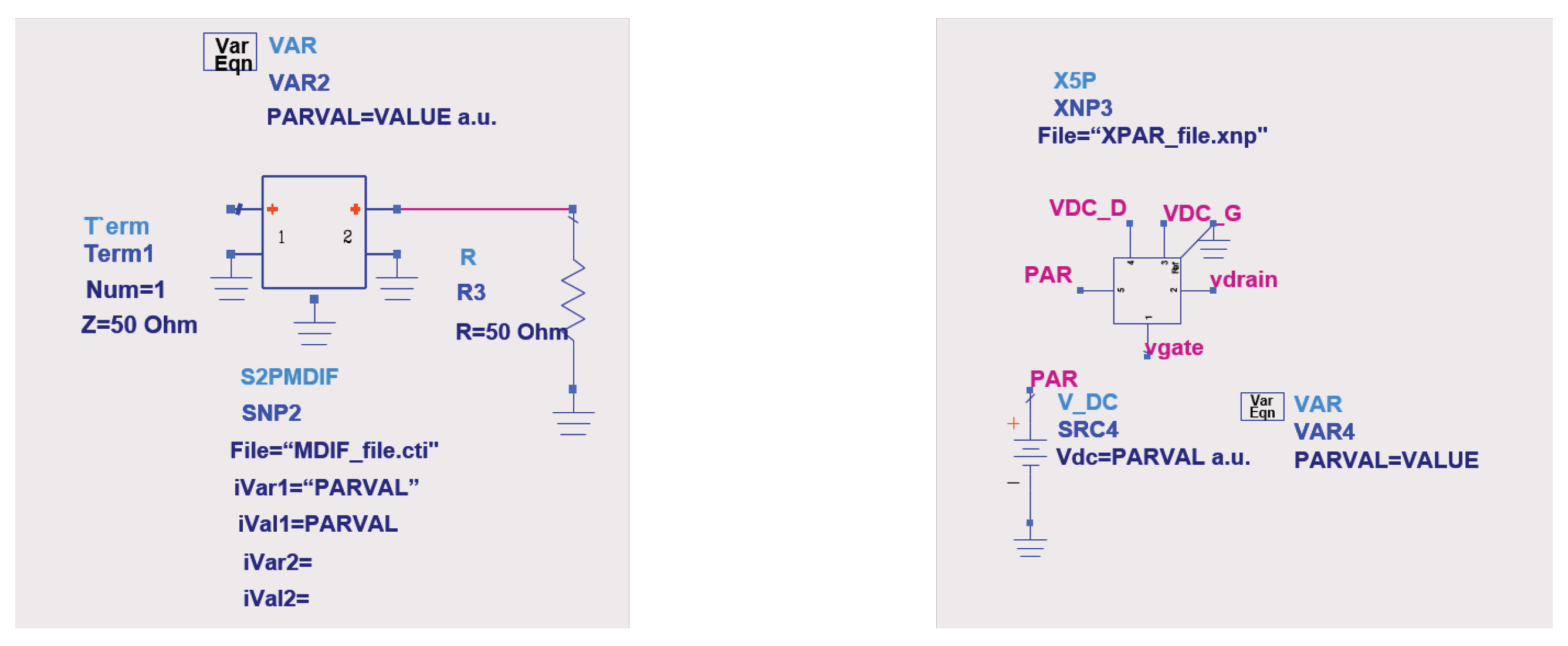
Figure 2 shows how the parameterized models (
1) and (
2) can be imported in Keysight ADS with standard circuit components readily allowing for statistical analysis using the built-in MC analysis capability.
3. Single-Stage Power Amplifier
In the particular case of a single-stage PA circuit, the nonlinear block is a 2-port representing the active device (usually an FET, with the gate-source terminals acting as the input port and the drain-source terminals as the output port), while the linear part counts two 1-port blocks representing, respectively, the Input Matching Network (IMN, possibly including device stabilization) along with the corresponding input signal generator, and the Output Matching Network (OMN) terminated by the stage load. These are directly connected to the gate and drain ports of the nonlinear block. Notice that, from the variability analysis standpoint, the gate and drain bias networks can be neglected since they are designed to be ineffective in the operating bandwidth independently of process variations (they may impact on low-frequency PA stability, which is out of the scope of the present work).
An important part of the statistical/yield analysis concerns the relative importance of process variability in the passive structures versus the active devices. In fact, the designer can optimize only the passives layout, while no or very limited changes to the active device structure (e.g., the number of fingers, or the via hole position) are allowed, thus making the active device PIV the ultimate limit to circuit optimization. A PIV aware design aims at identifying the main sources of variability, distinguishing not only between active and passive blocks, but also weighting the relative impact of each specific sub-block, thus identifying critical circuit sections. With this information the designer can try to optimize circuit robustness by minimizing the spread. On the other hand, if the active device variations distinctly dominate the overall PA performance spread, any effort directed to optimize the matching networks may result in no visible improvement.
The first design example we report is a deep class-AB tuned-load power amplifier at 12 GHz in GaAs MMIC technology. The active device is an epitaxial MESFET with a 170 nm-thick active layer doped with
. All details of the technology can be found in Ref. [
4]. TCAD physical simulations of the active device have been carried out in 2D and scaled to a 1 mm gate periphery, i.e., the gate width used for the PA design. The drain bias is 8 V, while the gate bias is selected to have a quiescent drain current of
. The load-line approach is used to define a preliminary estimate of the PA optimum terminations, and to tune out the output capacitance extracted from the
small-signal parameter. TCAD LS load-pull simulations have been then used to refine both the source and load impedance, achieving as final values
and
. On such loads, the PA can reach 27.5 dBm of saturated output power.
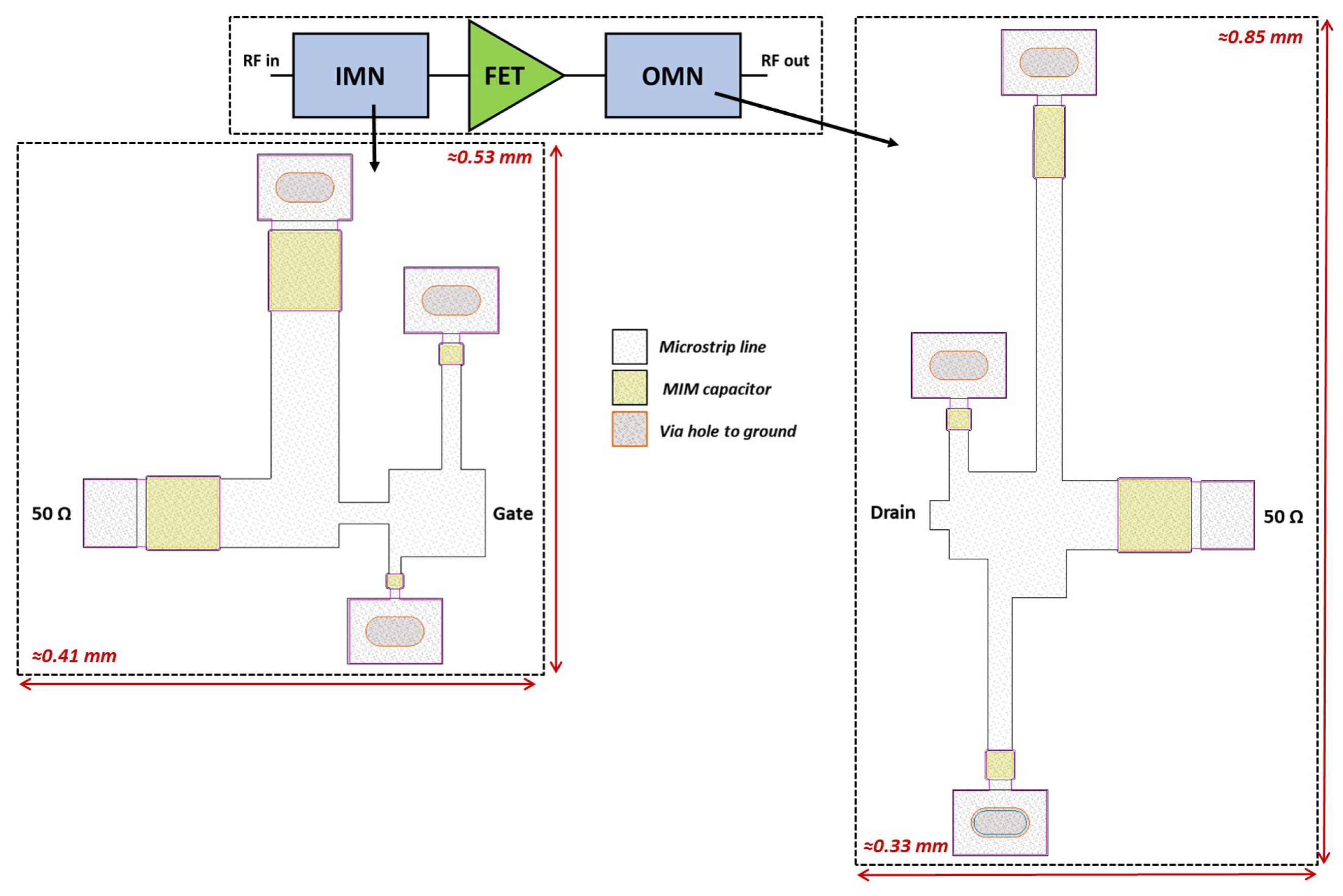
A commercial GaAs PDK for X-band applications is adopted to design the matching networks (more details in Ref. [
12]). The input and output matching networks (with nominal technological parameters), are designed by elaborating the preliminary design presented in Ref. [
15]. A semi-lumped approach is adopted, where MIM capacitors substitute large distributed components (long transmission line stubs) with the aim of reducing the overall PA size on wafer [
23]. Since the network behavior strongly depends on capacitor values, this solution is especially critical for PIV, given the non-negligible MIM spread predicted by the PDK. The final layouts of both the IMN and OMN are shown in
Figure 3.
We assume that the main sources of PA variability are the MIM layer thickness and the active device doping. According to the PDK, the dielectric layer thickness
is affected by a statistical spread, described by a Gaussian distribution with 2 nm standard deviation around the nominal 100 nm value, resulting in a corresponding spread of the MIM capacitance value. Doping variations are assumed to be uniform in the device, therefore doping level is treated as a statistical parameter described by a Gaussian distribution with 2% standard deviation around the nominal value. EM simulations of the IMN and OMN networks with varying
are carried out to extract the corresponding MDIF model parameterized by the MIM thickness, as explained in
Section 2. In the same way, TCAD physical simulations with varying doping concentration [
24], are used to extract the X-par device model parameterized by
. For the latter, the device bias and loading condition have been kept constant (nominal bias,
source impedance, and
load at drain).
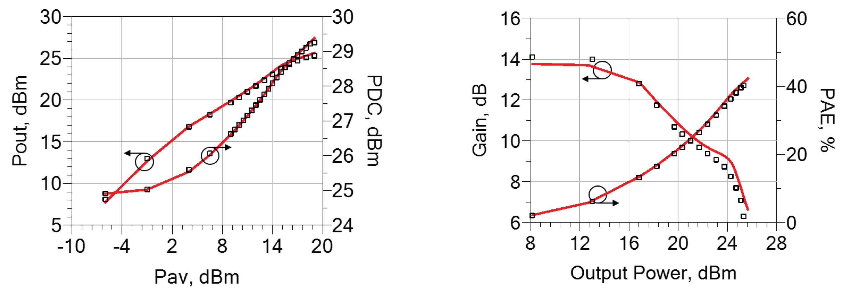
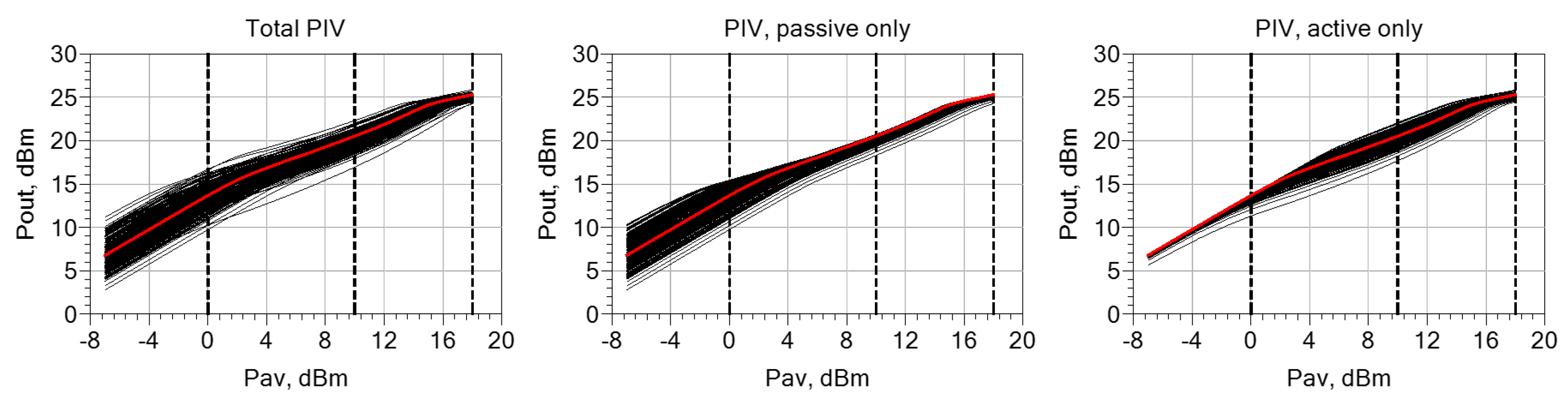
The final amplifier with nominal technological parameters exhibits 25.6 dBm of saturated output power, 13.8 dB linear gain and roughly 40% PAE, see
Figure 4, where the results from ADS simulations, extracted using the behavioral models for both the active and passive structures with nominal parameters are also compared to the corresponding TCAD simulations in order to demonstrate the accuracy of the developed models.
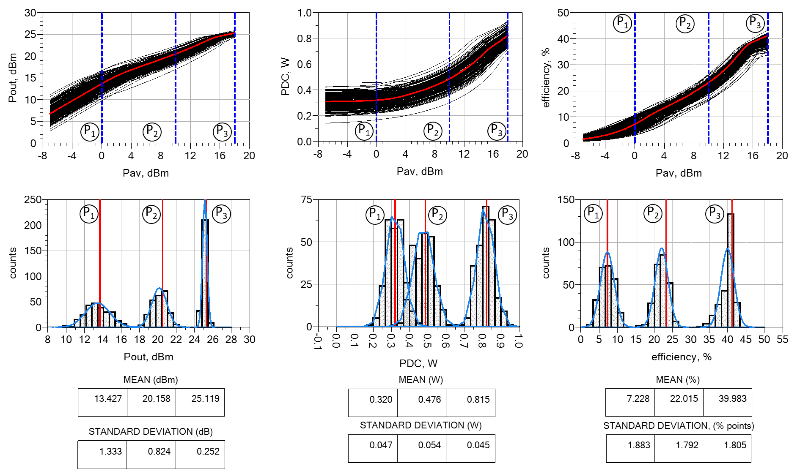
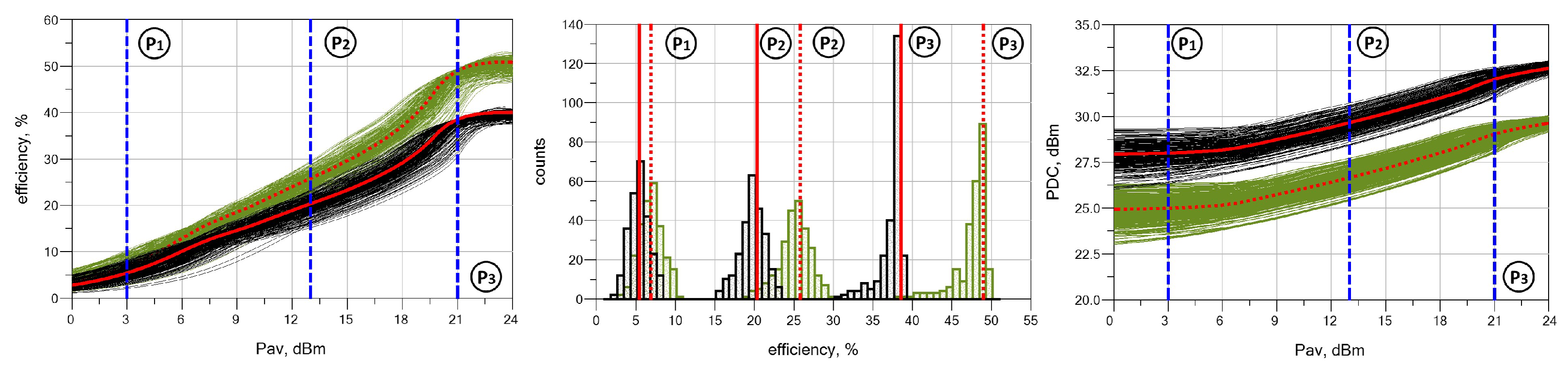
Statistical analysis has been carried out to investigate the PA design robustness towards process variability, allowing all the randomly varying parameters to change simultaneously, i.e., we create an ensemble of 250 randomized PA circuits with the two variable parameters (MIM thickness) and (doping) taking uncorrelated values out of their specific Gaussian distributions. Although the available input power is swept over 50 points from back-off to compression for each MC iteration, the complete simulation over 250 trials took only a few minutes in Keysight ADS, owing to the efficiency of the behavioral models used.
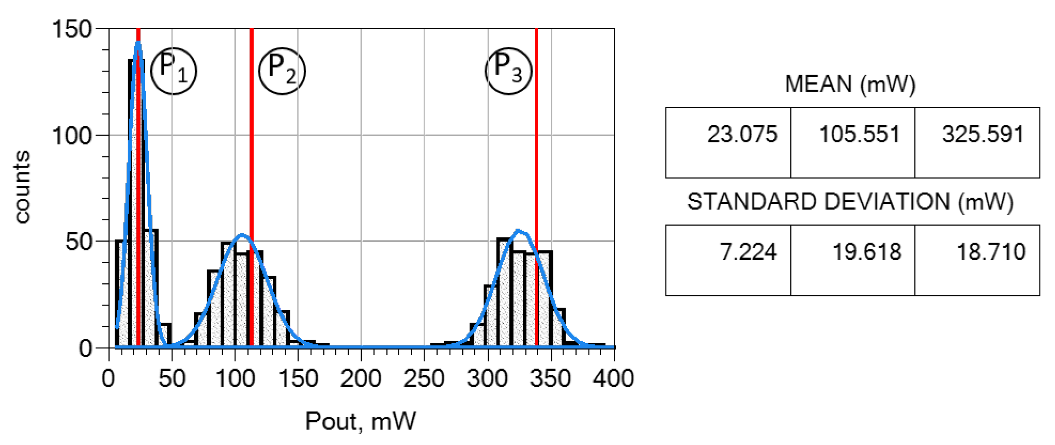
Figure 5 shows the results of the statistical analysis compared to the ones calculated with the nominal parameter values (red lines). We analyze in particular three significant input drive conditions (dashed blue lines): deep back-off (
dBm) labeled P
1, 5 dB of Output Power Back-off (OBO,
dBm) labeled P
2, and saturation (
dBm) labeled P
3. The histogram plots at the bottom of
Figure 5 allow for a precise estimate of the PA performance spread. We also report (cyan curves) the normal distributions fitting the statistical data, along with the corresponding average and standard deviation (STD). For higher input power a significant skew is observed and the normal distribution, being symmetric, may only represent a poor interpolation of the numerical data; nonetheless, the reported standard deviations provide, as a first approximation, a synthetic view of the main trends of the PA performance variations. More accurate interpolations with non symmetric distributions (e.g., the Weibull one) can be used to further extract compact models of PIV, but are beyond the aim of this work.
Concerning the output power (
Figure 5-left), we show the spread in dBm. Notice that this is a representation of the
relative spread. In fact, if we denote with
the output power, where
is the nominal output power and
the corresponding spread, we have
The relative spread
(
Figure 5, left) is maximum in back-off, up to 6 dB, and decreases in saturation to 1.55 dBm. Correspondingly, the
STD decreases from 1.33 dB at P
1 to 0.25 dB at P
3. To understand the reduction of
, we show in
Figure 6 the output power distribution in mW, highlighting that the absolute spread of
remains instead almost constant to a STD around 19 mW for input powers P
2 and P
3.
Turning back to
Figure 5, the spread of the DC power consumption (
Figure 5, center) and of the efficiency (
Figure 5, right) are instead found to be quite insensitive to the input power. The DC power STD remains roughly fixed around 50 mW and the efficiency around 2 percentage points.
We notice a pronounced asymmetry, with respect to the nominal value, of the output power (in dBm) and of the efficiency at higher input drive (P3), whose distributions are extending mainly towards lower values. This result is not surprising: since the IMN and OMN have been designed to optimize the output power in saturation, any variation of the MIM thickness with a constant layout corresponds to a variation of the impedance seen at the device ports, leading to a corresponding de-tuning of the PA matching, and a degradation of the overall performance.
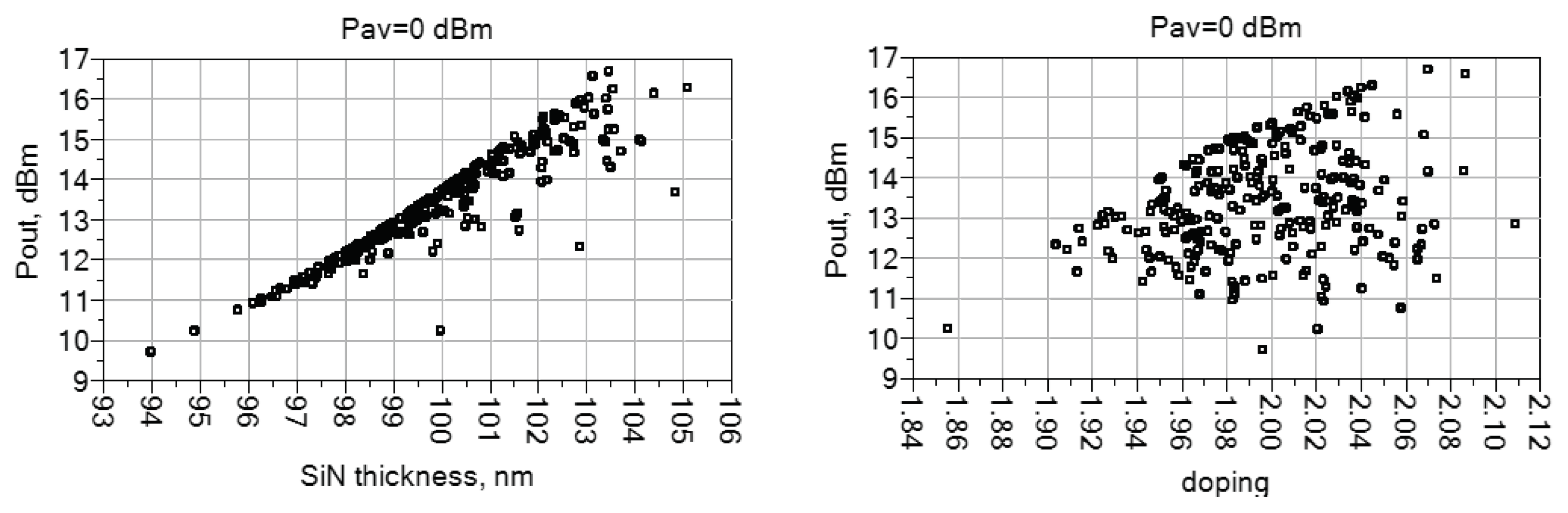
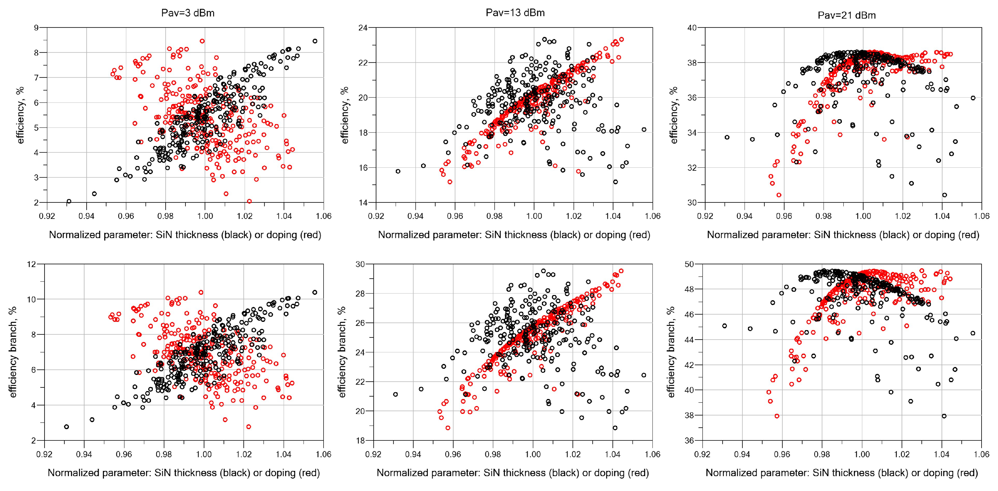
To assess the relative importance of PIV in the active device and in the passive structures,
Figure 7 and
Figure 8 report the correlation plots of the output power as a function of the individual variations of the two functional blocks.
Figure 7 refers to the back-off condition previously denoted with P
1: it is clear that the output power spread shows a tight correlation with the MIM thickness, while there is little correlation with doping. Hence, in this case the PA performance spread is dominated by the passives. The output power is roughly increasing with
, and, overall, the values are distributed symmetrically around the nominal one, obtained when
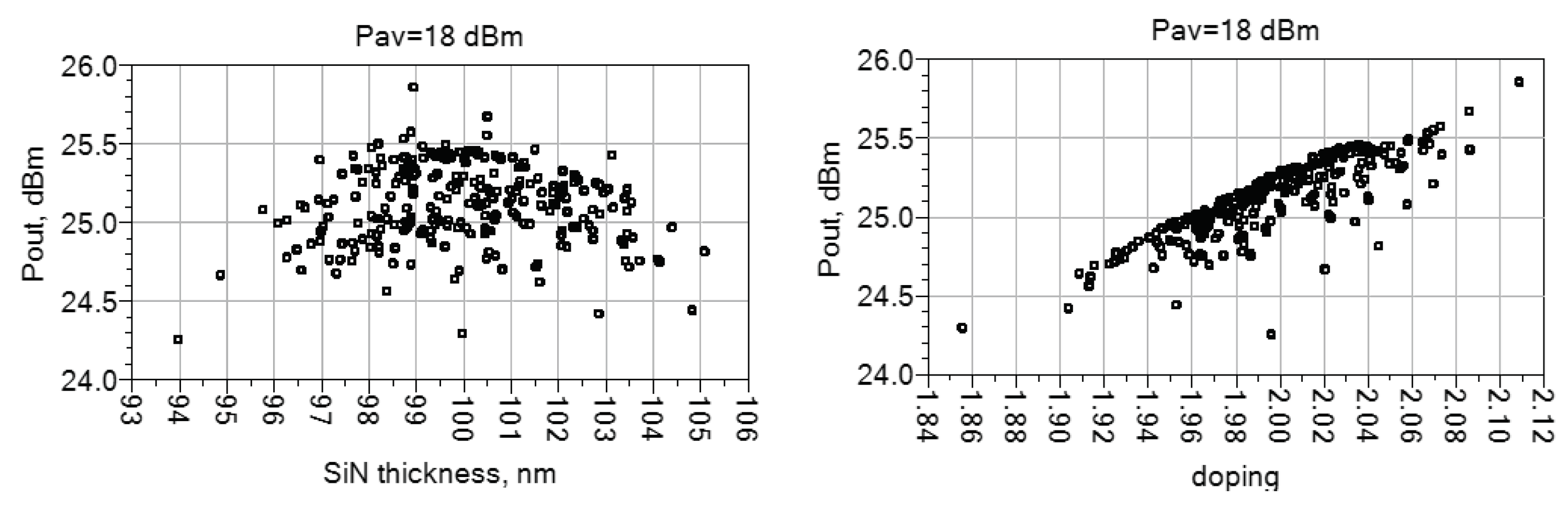
nm. An opposite trend is observed at higher power, e.g., for P
3, as shown in
Figure 8. Here the output power is tightly correlated with the doping variations, while little influence coming from the MIM layer thickness. The trend shows that the output power increases with doping. Interestingly,
Figure 8 (left) shows that, despite being loosely correlated, the output power is always lower with respect to the nominal value at
nm. This confirms that, when the MIM layer deviates from the nominal value, the designed OMN and IMN will exhibit port impedances progressively deviating from the optimum values required for maximum output power.
Correlation plots are a powerful tool to assess the relative importance of multiple concurrent statistical input, but they become difficult to interpret when more than two, and possibly correlated, sources of variations are considered. This is the reason why characterization data from the foundry are extremely difficult to interpret, requiring sophisticated regression analysis to sort out the effect of each individual variation. However, when it comes to the simulation level, it is very simple to run multiple simulations where statistical parameters are varied separately. As an example, we carried out the Monte Carlo analysis varying doping and
separately.
Figure 9 clearly shows that variations of the SiN layer (
Figure 9, center) impact more in back-off, where the distribution is also symmetric around the nominal value, while the impact at saturation is more limited and the predicted output power is distributed towards lower values with respect to the nominal one. Doping variations (
Figure 9, right) affect the overall power mostly in saturation, leading to a symmetric distribution: in fact, the nominal device doping does not represent an optimum value for the output power, which instead increases with doping. These results confirm the outcomes of the concurrent analysis reported in
Figure 7 and
Figure 8. However, thanks to the block-wise models, more sophisticated analyses can be carried out, to individuate the most critical block.
Focusing on the passives, an important information for the designer is to sort out whether the IMN or the OMN are further affecting the overall spread due to MIM variations. In order to assess this, we can simply run separate simulations where the
value is randomized only in the IMN or in the OMN, separately.
Figure 10 shows the outcomes of these simulations in the form of correlation plots. Interestingly, in back-off (
Figure 10, left), the spread is entirely correlated to the spread of the output impedance (OMN PIV, black symbols). With increasing input power, the role of the input mismatch (IMN PIV, red symbols) becomes increasingly significant and at saturation the two networks play approximately the same role. This suggests that the IMN is possibly under-optimized at all power levels, while the OMN is well centered at saturation. To summarize, the overall performance variations due to the passives is much lower than that due to doping at saturation, but, for a back-off operated PA, these results clearly indicate that a re-design/optimization of the OMN can bring a significant improvement in the MMIC robustness against PIV, hence increasing the expected yield.
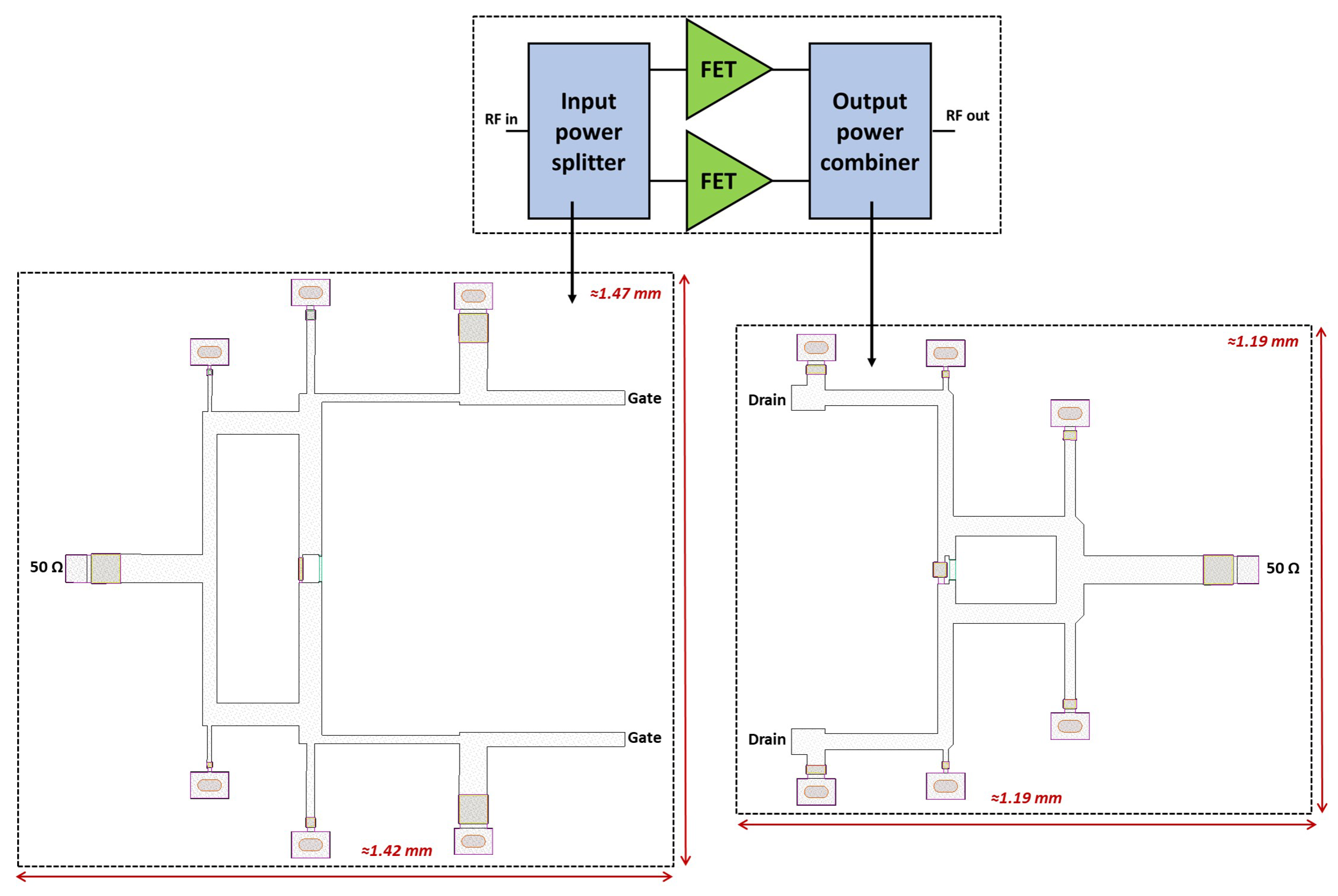
4. Combined Power Amplifier
As a further demonstration of the proposed approach we also designed a combined PA, where two FET devices are connected in parallel. The same device of the single-stage PA of
Section 3 is considered, with the same bias, and the same doping-dependent statistical model. At the input and at the output, two 3 dB isolated dividers are adopted to evenly split and recombine the input and output signals to/from the two identical branch PA and to provide the necessary matching. The two dividers have been designed according to the strategy proposed in Ref. [
25]. The device distance is set to roughly 0.9 mm. First, a symmetric combiner composed of three line-stub sections has been designed to provide matching at all ports. As shown in
Figure 11, reporting the final layouts, a semi-lumped approach is adopted, as for the single-stage matching networks, with distributed transmission lines and shunt MIM capacitors as stubs. The isolation impedance is then computed with the formulas in Ref. [
25] and implemented as a parallel
block, adopting an MIM capacitor and a thin-film TaN resistor.
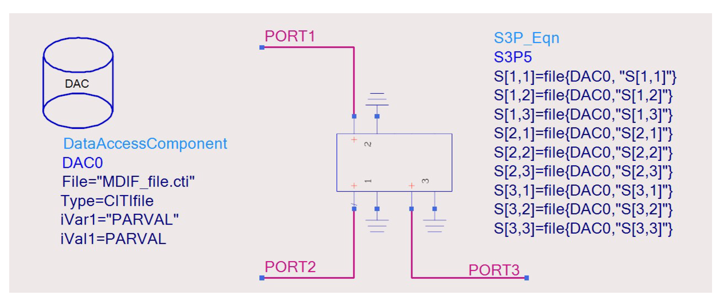
Additionally in this case, the thickness of the SiN layer forming the MIM capacitors has been selected as the main contribution to passive PIV, thus a parameterized 3-port S-parameter model has been created for both the input and output combiner, from EM simulations, at a few selected values. Note that, while for a 2-port MDIF file a specific component exist in Keysight ADS (see
Figure 2), for a 3-port the more general Data Access Component must be adopted, as shown in
Figure 12. As mentioned before, each of the two active devices is described by the same X-parameter model extracted from TCAD simulations and used for the single-stage PA, considering channel doping fluctuations as the only (main) source of PIV.
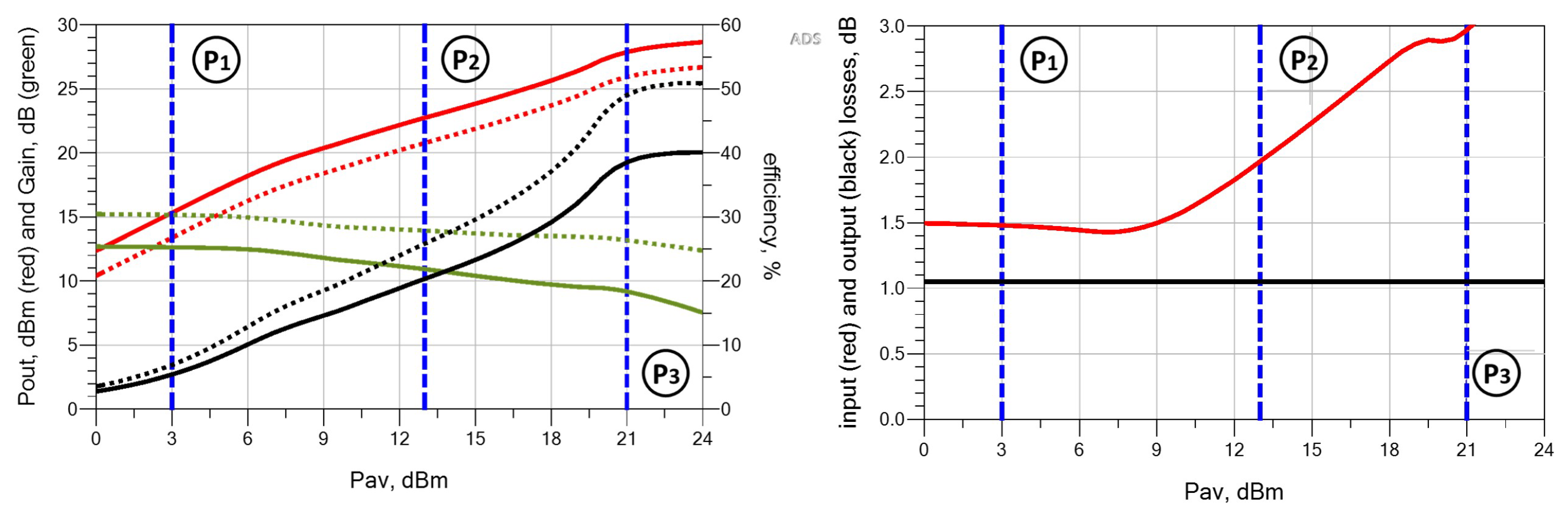
Figure 13 (left) reports the performance of the combined PA with the nominal values for the two parameters (device doping and SiN thickness). The performance power of each separate branch PA (dashed lines) is also reported to highlight the effect of the combined structures. The synthesized load, namely
, is slightly different to the optimum one chosen for the single-stage PA and favors gain and efficiency rather than output power; in fact, each branch shows a small-signal gain in excess of 15 dB and 50% of saturated drain efficiency, while the saturated output power is below 26 dBm. The combined PA increases the output power of 2 dB, thus achieving nearly 28 dBm at saturation with an efficiency around 40%. With respect to an ideal combination (3 dB), the combiner introduces a 1 dB loss (ratio of the combiner’s output and incident power) constant with input power, as shown in
Figure 13 (right, black curve). The total small signal power gain is 12.6 dB, but, since the input combiner losses (ratio of the combiner’s output and incident power) are not constant with input power drive (
Figure 13, right, red curve), the shape of the curve is different from that of the single device at high input power. The three blue dashed lines show the 3 points P
1 (small-signal, P
dBm), P
2 (5 dB OBO, P
dBm), and P
3 (saturation, P
dBm) considered for the statistical analysis of the PA performance.
Similarly to the single-stage PA case, we run a 250-trial Monte Carlo analysis of the combined PA with swept input power, considering uncorrelated variations of SiN layer thickness and device doping, both with 2%-standard-deviation Gaussian distribution. The results of this statistical analysis are reported in the following.
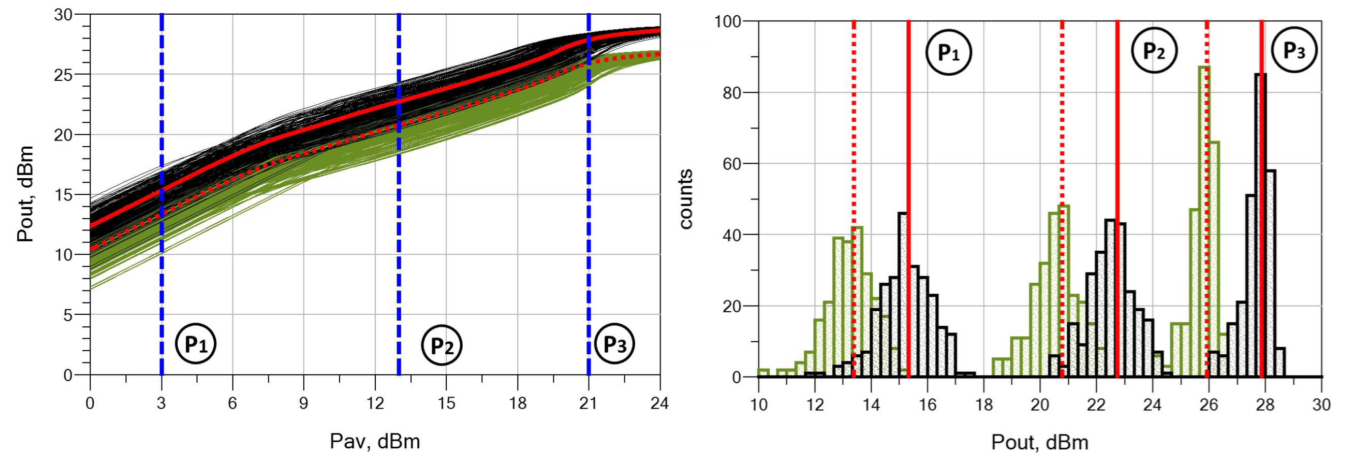
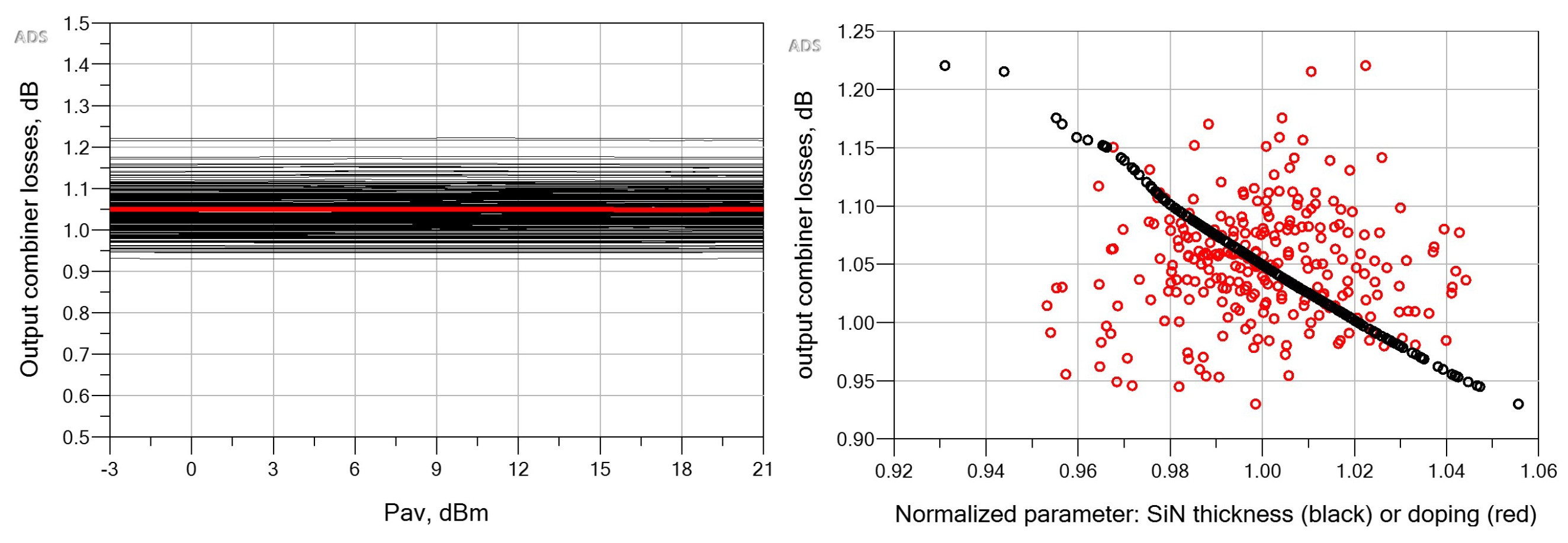
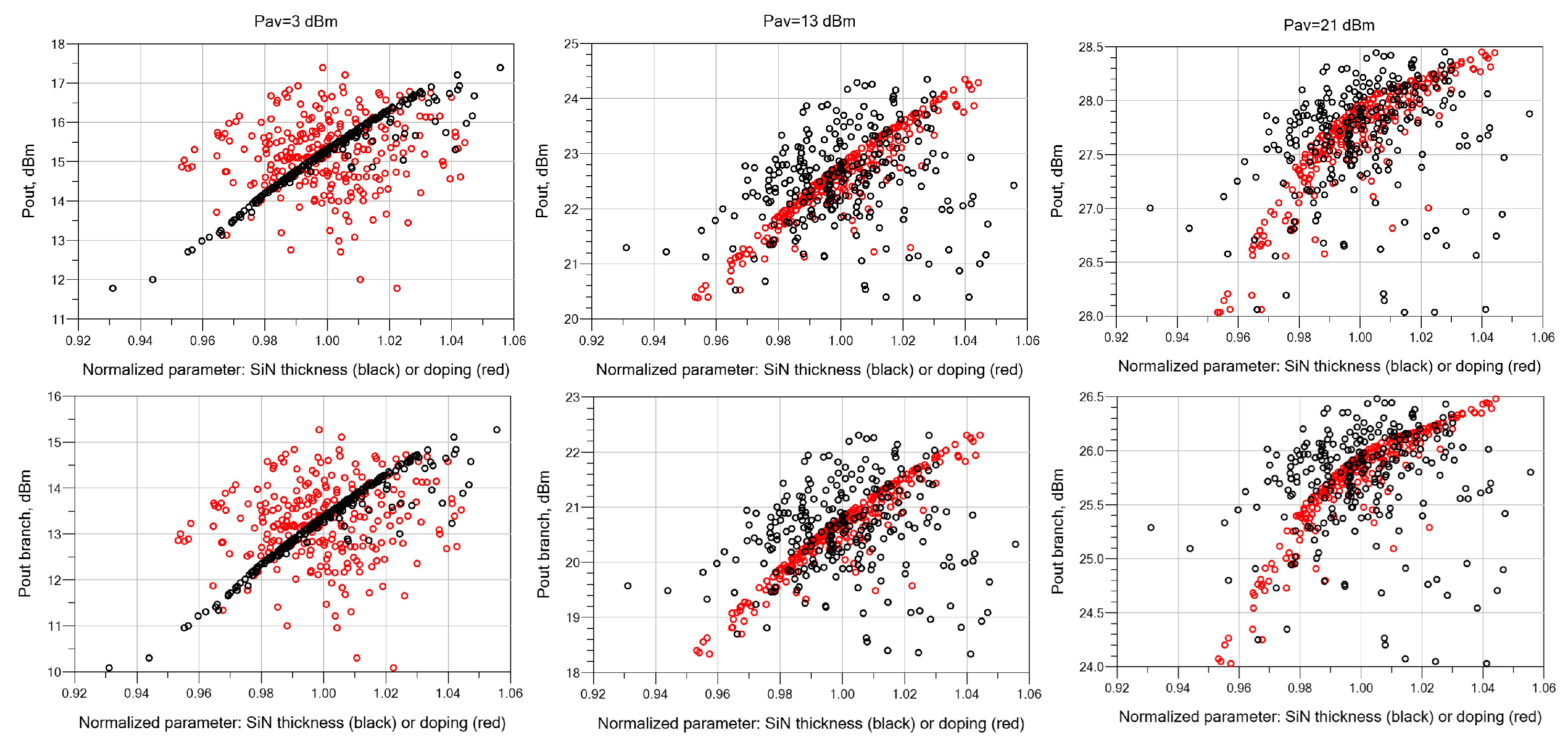
Figure 14 shows the results concerning the output power: both the total output power (black curves, red solid line for nominal values) and the single branch output power (green curves, red dotted line for nominal values) are considered. As can be noted, PIV impacts in the same way both the single and total output power: both the family of input-output curves and the histograms are identical, except for a shift in the output power. This means that the output combiner losses are constant with input power drive, as confirmed by the results reported in
Figure 15 (left). As expected, these variations are correlated only to SiN thickness fluctuations at all power levels, as shown in
Figure 15 (right) (only one input power level shown for brevity). The relative output power spread due to PIV can be up to 4 dB, hence more than the power increase brought by device combination (3 dB): this should be taken into account in the design phase, considering sufficient margins with respect to target specifications, to accommodate for variations.
Additionally, the correlation between the output power and the two sources of variations is nearly the same for the branch and full PA, apart from the output power shift. The trend is similar, but even more marked, to what is found for the single-stage PA (
Figure 7,
Figure 8 and
Figure 9). As shown in
Figure 16, the output power spread in small-signal conditions is almost completely due to the passives, while at higher power it becomes much more correlated to the device doping. At saturation the total spread is very small, skewed toward lower output power, and still mainly correlated to doping concentration.
In
Figure 17 (left/center), the statistical results for the drain efficiency are reported. The efficiency spread is both due to the spread in the output power and to the spread in the DC power consumption, shown in
Figure 17 (right).
Additionally in this case, the results of the entire PA are compared to those of the single branch: as the output power case, the statistical distributions, as well as the correlation with the different sources of PIV, shown in
Figure 18, are very similar, thanks to the same branch and total DC power statistical spreads. As shown in
Figure 18, the efficiency is slightly more dependent on passives in the small-signal, while it becomes dominated by device doping at medium power, and finally equally correlated with both at saturation. In general, the maximum efficiency spread is around 10%.
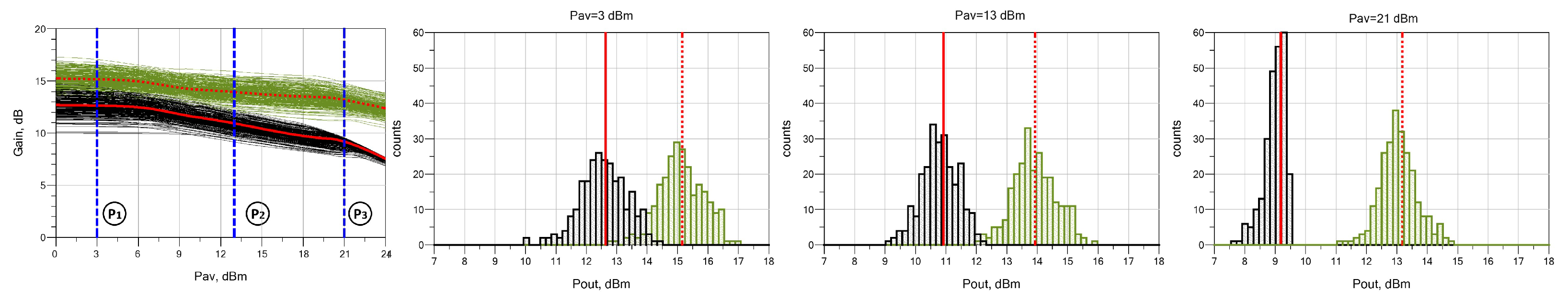
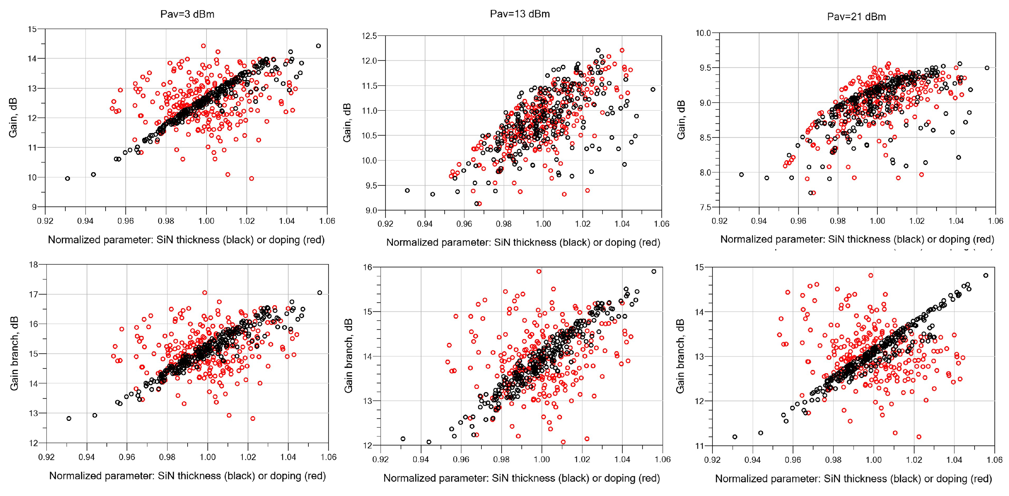
Figure 19 shows the results concerning the total power gain (black curves, red solid lines for nominal values) and the single branch gain (green curves, red dotted lines for nominal values). The latter accounts only for the active device and output load variations, hence the PIV impact is different: in particular, we can observe that at saturation the branch gain still shows a relatively large and symmetrical spread, while the total gain becomes neatly skewed toward lower values. In addition, the correlation of the spread with the two sources of variations is different when looking at the total gain with respect to the single transistor case, as reported in
Figure 20. The branch gain spread (bottom) is mainly due to the passives at all power levels. On the contrary, the total gain (top), is mainly correlated to the SiN thickness variation only in small-signal conditions, while the impact of doping in the active devices becomes increasingly large with input power. The total gain spread is significant (3 dB) at low and medium power levels, while it decreases down to roughly 1 dB at saturation.
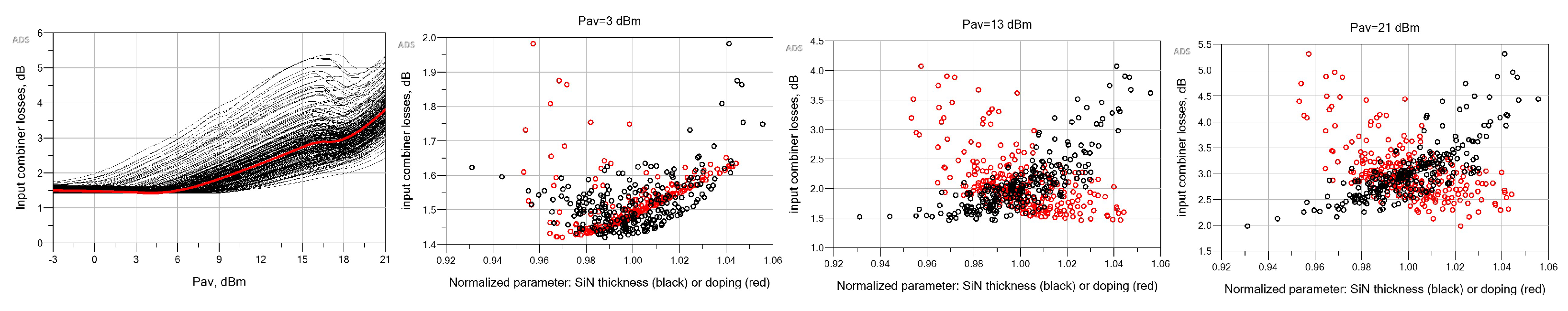
The different statistical behavior of the total and branch gains can be traced back to the input mismatch and to losses. As illustrated in
Figure 21 (right), the behavior with input power of the input combiner losses, included only in the total gain, is changed by PIV. At high input power, the losses become clearly skewed toward worse values, as the total gain in
Figure 19 (right). Interestingly, the input combiner losses are correlated to both active devices and MIM capacitors variations: the former is dominant in small-signal, while the latter at saturation.
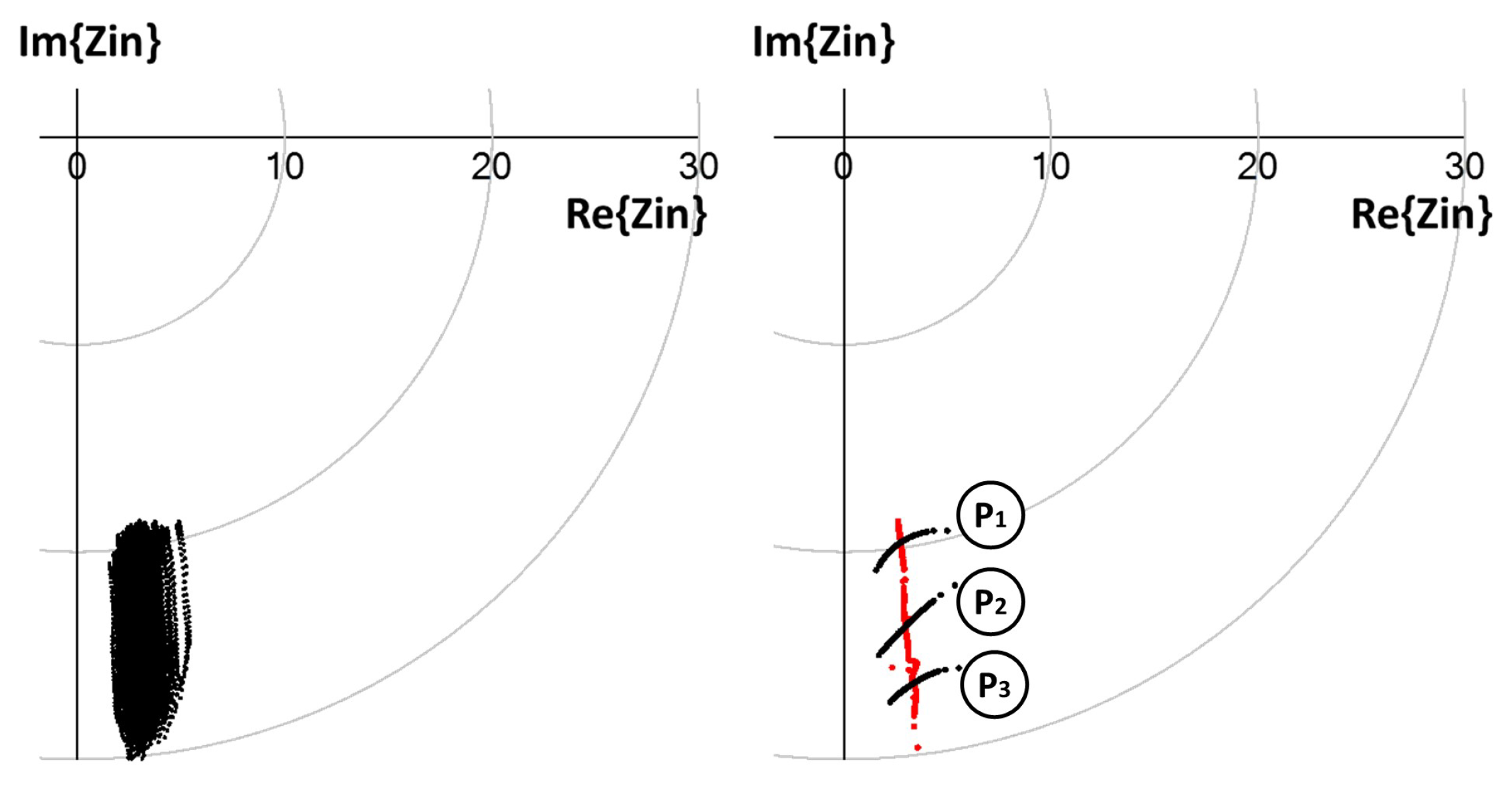
Besides the losses, the total gain differs from the branch gain also due to the input mismatch at the devices’ gates.
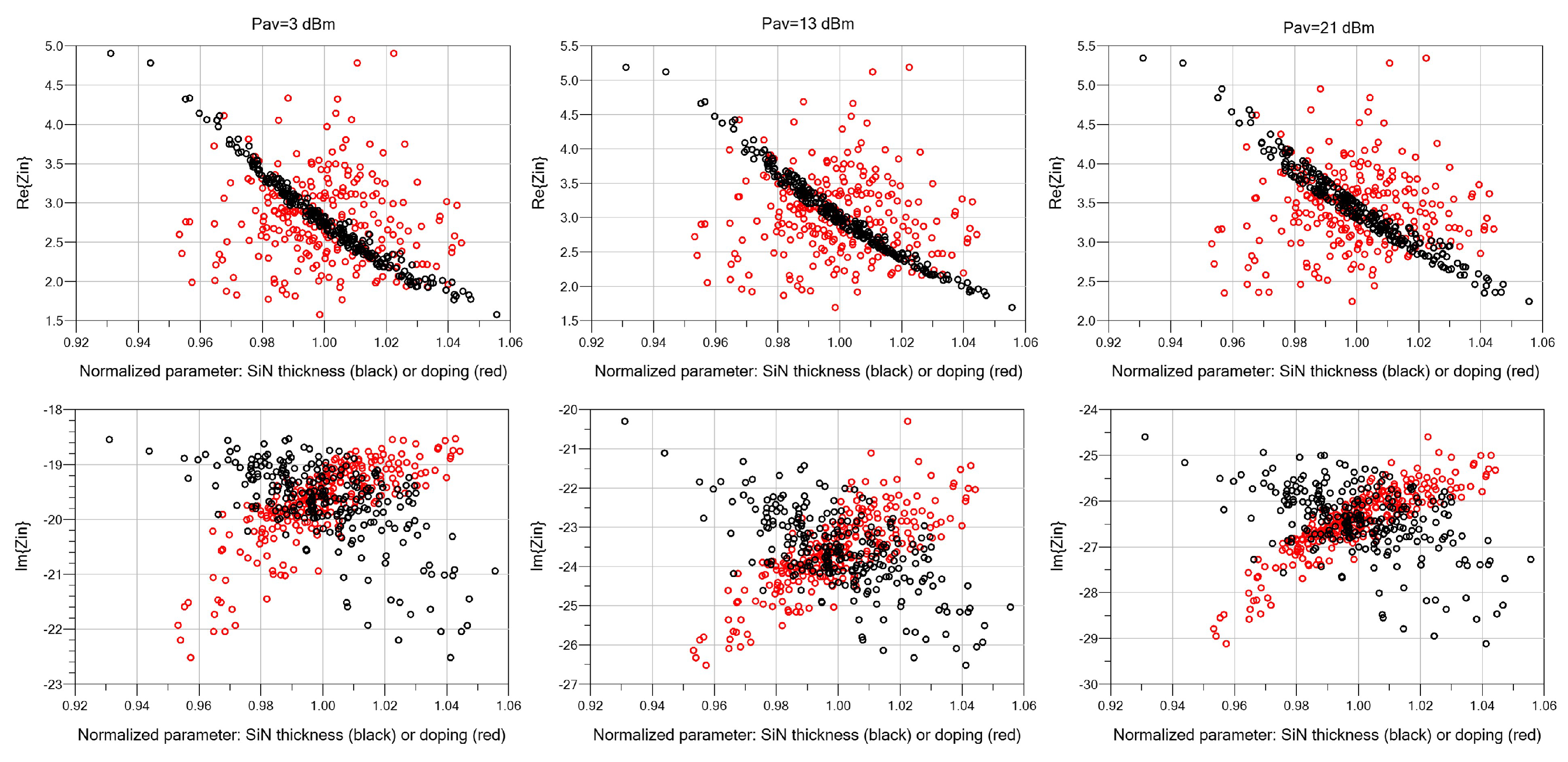
Figure 22 (left) reports the input impedance spread according to the total analyzed sources of variation, which is significantly changed by PIV. As can be noted from
Figure 22 (right) and
Figure 23, the doping mainly impacts on the input capacitance (imaginary part), as expected since doping determines the FET depletion capacitance, while the SiN thickness affects both the real and imaginary parts of the input impedance, due to the different load synthesized at the device terminals.
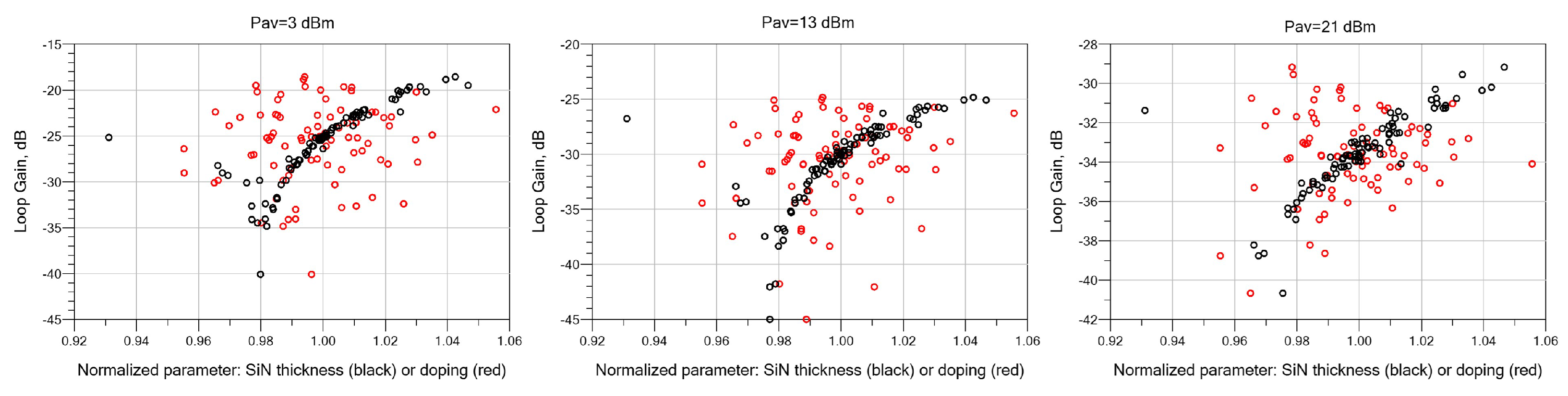
Finally, we checked the loop gain of the combined PA at 12 GHz, to verify the absence of potential odd-mode oscillations [
26,
27]. The results of the statistical analysis are reported in
Figure 24: the loop gain remains safely below
dB under concurrent doping and capacitance variations, and it is correlated to only the PIV in the passive networks. The complete stability analysis, which would require more sophisticated broadband/multi-frequency models for both active and passive devices, is beyond the scope of this work.


