Article

Space-Compliant Design of a Millimeter-Wave GaN-on-Si Stacked Power Amplifier Cell through Electro-Magnetic and Thermal Simulations

1
Department Electronics and Telecommunications, Politecnico di Torino, 10129 Torino, Italy
2
Microwave Engineering Center for Space Applications (MECSA), 00133 Roma, Italy
3
Department Electrical Electronic Information Engineering, Università Bologna, 40126 Bologna, Italy
4
Department Electronic Engineering, Università Degli Studi di Roma Tor Vergata, 00133 Roma, Italy
*
Author to whom correspondence should be addressed.
Electronics 2021, 10(15), 1784; https://doi.org/10.3390/electronics10151784
Submission received: 25 June 2021 / Revised: 21 July 2021 / Accepted: 23 July 2021 / Published: 26 July 2021

Abstract

:
The stacked power amplifier is a widely adopted solution in CMOS technology to overcome breakdown limits. Its application to compound semiconductor technology is instead rather limited especially at very high frequency, where device parasitic reactances make the design extremely challenging, and in gallium nitride technology, which already offers high breakdown voltages. Indeed, the stacked topology can also be advantageous in such scenarios as it can enhance gain and chip compactness. Moreover, the higher supply voltages and lower supply currents beneficially impact on reliability, thus making the stacked configuration an attractive solution for space applications. This paper details the design of two stacked cells, differing in their inter-stage matching strategy, conceived for space applications at Ka-band in 100 nm GaN-on-Si technology. In particular, the design challenges related to the thermal constraints posed by space reliability and to the electro-magnetic cross-talk issues that may arise at millimeter-wave frequencies are discussed. The best cell achieves at saturation, in simulation, 3 W of output power at 36 GHz with associated gain and efficiency in excess of 7 dB and 35%, respectively.

1. Introduction

Millimeter-wave (mmW) frequencies are becoming a reference frequency range for both terrestrial and space applications [1,2,3,4,5], allowing for improved data rates and more efficient modulation schemes.
Solid-state power amplifiers based on gallium nitride (GaN) monolithic microwave integrated circuit (MMIC) technology have gained great interest as a potential replacement for traveling wave tube amplifiers (TWTAs) in many different space applications. In fact, despite a lower efficiency, they can provide high power densities, in the order of several watts per millimeter [2], at lower cost, lower supply voltage and in a reduced chip area. Moreover, graceful degradation and selectable form factor represent significant benefits for space applications [6]. Hence, developing efficient and compact space-compliant MMIC PAs at Ka-band (26.5–40 GHz) is a hot research target. Long-term reliability is a major requirement of electronic equipment to be deployed on-board satellites, which must therefore be designed at strongly reduced stress with respect to the maximum technology limits. This procedure, known as space derating [7], requires limiting the PA’s currents and voltages and keeping the maximum device temperature sensibly lower with respect to terrestrial applications. According to the European Space Agency (ESA) directives, for satellite payloads, the maximum value of 160 ° C is considered for GaN devices [8]. This condition must be enforced in the worst case of maximum back-side temperature ( T BS ), which is typically as high as 80 ° C for satellite applications. Temperature constraints may thus become the most challenging design requirement, especially in the case of GaN-on-Si technologies, due to the poorer thermal properties of the silicon substrate with respect to silicon carbide [9].
At very high frequency, parasitic reactances play a crucial role and finger-to-finger phase misalignments may arise due to the different signal path length. Both must be kept as small as possible to avoid gain degradation, by reducing the size of the individual transistors in the PA. This in turn requires the combination of many devices to achieve a high output power. Classical amplifier topologies rely on parallel power combination, summing up the devices’ drain currents. This solution, however, requires a large chip area, thus increasing cost, and reduces the optimum source and load impedances, already typically low at mmW, with a detrimental effect on impedance matching.
An alternative approach is represented by series power combination, summing up devices’ drain-source voltages: a solution known as stacked PA [10]. This allows for a higher drain supply voltage, which represents a big advantage in low-breakdown technologies. Moreover, it keeps the input impedance unchanged while increasing that at the output, which is beneficial for matching. Moreover, chip area occupation is sensibly reduced since power combination is embedded in the architecture and does not require big external passive structures. Finally, this architecture increases power gain, which can also be a great benefit in GaN technology at mmW frequencies, where the maximum available gain of single devices is rather low.
In the literature, stacked PAs are largely exploited in CMOS technology [11,12,13,14,15,16,17,18], where the breakdown voltage is a major limit, but some examples can also be found in GaAs [19,20,21,22,23,24,25,26,27] and very few in GaN [28,29,30,31]. A main advantage of the stacked PA is that it can be profitably adopted as a basic high-power and high-gain cell to be further exploited in more complex PA architectures, from classical parallel combined PAs [32] to advanced architectures such as distributed PAs [33], spatially-combined PAs [34] and Doherty PAs [30,35]. In this perspective, the stacked cell is treated as a three-terminal “macro-device” [36]. However, to attain this, a self-bias approach must be pursued, to avoid additional bias lines for the gates of the stacked stages, which would increase the complexity of bias routing when combining more cells.
At very high frequency, designing a stacked PA is made extremely challenging by device parasitics, which cause phase de-tuning among stages and must therefore be properly compensated by means of inter-stage matching networks. The latter must be carefully optimized in order to limit losses, and, for high compactness, their design must strongly rely on extensive electro-magnetic (EM) simulations to avoid overlooking possible detrimental cross-talk effects [37].
This work discusses the design methodology of a space-compliant self-biased Ka-band stacked cell, by reporting two design examples at 36 GHz based on a commercial 100 nm GaN-on-Si technology. These cells, differing for the inter-stage matching strategy, have been developed in the framework of a wider project aiming at the design of narrow-band (<1 GHz), high-power amplifiers at 36 GHz for space applications, adopting the stacked cell as a building block for more complex PA structures. To this aim, layout compactness and ease of integration of the cell, thus a self-bias approach, are considered as further design requirements to be fulfilled. The target output power for the stacked cell is in the order of few watts ( 33 dBm). The most relevant steps of the thermal analysis, crucial for space applications, are recalled and the entire design procedure are reported step by step. Due to the high frequency and layout compactness, both cells required extensive EM simulations and the one first introduced in [31] was finally selected, which achieves in simulation, at saturation, 3 W of output power at 36 GHz with associated gain and efficiency in excess of 7 dB and 35%, respectively.

2. Stacked PA Architecture

The schematic of a N-device stacked PA is shown in Figure 1: it is composed of a first common source (CS) stage, cascaded by ( N 1 ) pseudo-common-gate (or degenerated common gate) stages, indicated simply as CG for convenience. The latter differ from standard CGs because of the gate capacitances, which are not simply short-circuits at the operating frequency, as in cascode PAs, but instead play a crucial role in device matching. As shown in Figure 2, reporting a simplified equivalent intrinsic circuit for the CG stage where all parasitics are neglected except for C gs , they form a capacitive voltage divider with the intrinsic input capacitance, allowing for device inter-stage matching and voltage waveform alignment.
As highlighted in Figure 1, the maximum output power is reached when the load that each nth transistor sees between its drain and source terminals is equal to the optimum one ( Z ds , n = Z opt ), or, equivalently, when its output load (from drain to ground) is Z L , n = Z in , ( n + 1 ) = n Z opt . Both the input and the drain-source impedances of each nth CG stage depend on the external (added) gate capacitance C g , n as
Y in , CG n = 1 Z in , CG n = i in v in = g m A n + j ω C gs A n
and
Z ds , CG n = v ds i ds = Z L , n A n g m
where
A n = 1 + C gs C g , n
Note that Z ds , CG n is always independent from the impedance connected at the source terminal, while Z in , CG n does not depend on the output load Z L , n in this simplified circuit, but it actually does when also considering other parasitics, since the transistor is no longer unilateral.
To provide maximum output power, the device must be loaded at the intrinsic drain-source plane by the optimum load R opt that simultaneously maximizes voltage and current swings. By posing Z ds , n = R opt and Z L , n = n R opt , we obtain
C g , n = C gs ( n 1 ) g m R opt 1
which is the classical design equation of the stacked PA [38]. From (1), we can note that this value of C g , n also provides matching for the real part of Y in , CG n :
{ Y in , n } = g m A n = 1 ( n 1 ) R opt
However, we also have a non-zero imaginary part directly proportional to the operating frequency f; in fact,
Y in , n = 1 ( n 1 ) R opt 1 + j ω C gs g m 1 ( n 1 ) R opt 1 + j f f T
where f T g m 2 π C gs is the device cut-off frequency.
Substituting (6) into (2) gives
Z ds , n = Z L , n + 1 ( n 1 ) R opt = R opt 1 n 1 + j f T f 1 + f T 2 f 2
meaning that, for the same operating frequency, the mismatch due to C gs depends on n and thus is increasingly worse moving along the stacked chain. A non-zero imaginary part in the load Z ds , n yields a phase misalignment between current and voltage and limits the maximum current swing thus reducing the maximum achievable power.
At very high frequency, the device output capacitance also becomes significant, asking for inductive compensation [22], and waveform de-phasing across stages is experienced, due to the combined effect of parasitics and phase rotation along interconnection lines. Therefore, an additional inter-stage matching network (ISMN) becomes mandatory, to provide impedance matching, recover phase misalignments and achieve proper operation of the stacked devices.
For ISMN design, two different approaches are possible: a theoretical approach, where the analysis of the structure is carried out considering parasitics in order to find adequate design guidelines or formulas, as in [11,22,27], or a load-pull approach, where the (complex) optimum extrinsic load Z opt , gathered from load-pull simulations or measurements, is adopted for the design. In the theoretical approach, the values of the device parasitics must be known, extracted either from simulations or measurements [39], and some simplifying assumptions are usually made, neglecting some parasitics (e.g., inductive parasitics) and, above all, their non-linear behavior with input power (non-linear capacitances). The latter makes this approach approximated, thus requiring post-optimization based on device non-linear models. On the contrary, the simulated load-pull approach fully exploits the non-linear device models, implicitly taking into account both linear parasitics and non-linear effects, with a level of accuracy that depends only on the model itself. Since accounting for parasitic effects is complex at very high frequency, in this work, the load-pull approach is followed.

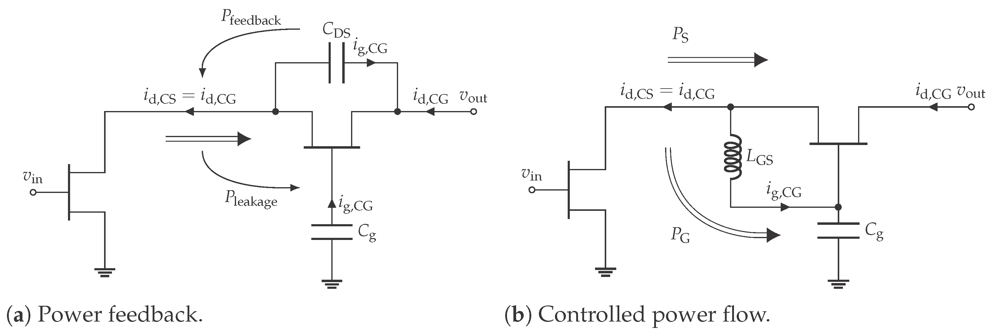
Gate Power Leakage and Maximum N

The presence of the gate capacitances C g , n implies that part of the output signal of the preceding stage is drawn toward the gate of the subsequent one in order to drive it, as depicted in Figure 1. This phenomenon is often referred to as gate leakage or gate power leakage to highlight that it is responsible for sub-optimum power combination in the basic stacked PA [10].
Moreover, as demonstrated in [40], the need of a gate current to drive each CG stage makes the maximum number of transistors that can be stacked limited by the technology cut-off frequency, f T . In fact, given that i d , n = i s , n i g , n , the current gain of the nth CG stage is
β CG , n = | i d , n | | i s , n | = 1 1 + | i g , n | | i d , n | = 1 1 + 1 β CS = f T f T + f
since
β CS = | i d , 1 | | i g , 1 | = g m V gs 2 π f C gs V gs = f T f
Thus, each CG added to the stack introduces a loss in the total current gain and hence in the achievable output power
P out = N V DS , 1 · β CG , n ( N 1 ) I D , 1 = N β CG , n ( N 1 ) P out , CS
At a specific operating frequency f, the maximum number of devices that can be stacked is obtained from (10) as [40]
N max = 1 ln 1 + f f T
where · stands for rounding toward the lowest integer.

3. Technology

The technology selected for the project is the D01GH process from OMMIC: a 100 nm gate-length GaN-on-Si HEMT process with which different designs at the target frequencies have been successfully demonstrated in literature [2,4,5,41]. At European level and among commercial processes, this one features the shortest gate-length even if, for space applications, working with a Si substrate, rather than SiC, may represent an issue. Compared to SiC, Si shows a much lower thermal conductivity, almost three times lower in the 0–100 ° C range [9], but it is cheaper and might allow, in the future, for the integration of GaN-based RF and Si-based digital sub-systems onto a unique chip.
The main features of the selected process are summarized in Table 1. The quiescent drain-source voltage is reduced to 11.25 V. This choice guarantees that for a Class AB PA design the intrinsic dynamic load lines of the devices reach a peak drain-source voltage well below the maximum derated value (75% of the technology breakdown voltage). This reduces the output power density to 2.5 W/mm. Nevertheless, the most stringent limiting factor on achievable output power is represented by the maximum junction temperature of 160 ° C, 40 ° C below the maximum value indicated for reliable terrestrial applications.

3.1. Device Thermal Model

As the junction temperature is so critical for the present design, a reliable thermal model must be adopted to account for it. For design optimization, the model should be not only accurate, but also rather simple to enable fast simulation. A 3D thermal stack for finite-element (FEM) thermal simulation is given by the foundry. However, simulation times are incompatible with design optimization, thus 3D thermal simulations are used only to accurately assess the effective temperature of the final cell. During the design, instead, the junction temperature is kept under control by means of a simplified 1D heat-flow model.
The latter adopts a reference thermal resistance R th , REF , which is computed only once for a reference temperature value T REF , and is then used in the calculation of the junction temperature as [42]
T j = T BS   e R th , REF P diss T REF
where temperatures are expressed in Kelvin, T BS is the back-side temperature and P diss is the power dissipated in the transistor’s channel. With respect to the classical definition of thermal resistance ( R th = T j T BS / P diss ), R th , REF has the advantage that it can be considered approximately constant versus both T BS and T j as shown in Figure 3, while the thermal resistance nonlinear dependency on temperature is accounted for by the exponential function. In particular, for this process, R th , REF = 29 ° C/(W·mm) at T REF = 20 ° C, that, as can be seen in Figure 3, represents a worst-case value. By reversing (12), assuming the maximum T j = 160 ° C and T BS = 80 ° C, we obtain a maximum dissipated power density below 2.1 W/mm. For a SiC substrate, the value of R th , REF in this model would have been below 17 ° C/(W·mm), hence the maximum allowed dissipated power density within the space derating limits would have been around 3.5 W/mm.

4. Preliminary Design

With a cut-off frequency of 90 GHz, according to (11), only two devices can be stacked at 36 GHz. Thus, the cell is composed of just one CS stage and one CG stage, and its drain bias voltage and optimum output termination (under the assumption of ideal series combination) are two times higher than that of the CS alone.

4.1. Device Analysis

At Ka-band, the number of fingers of a transistor and their width need to be reasonably low to keep parasitic reactances small. Therefore, the largest possible device is the 8 × 75 μ m transistor, which has been adopted for the stacked cell.

4.1.1. DC Bias Point Selection

The DC characteristics of the chosen device in CS configuration at T BS = 80 ° C are reported in Figure 4: the maximum current for V DS = 11.25 V is roughly 600 mA. To achieve high efficiency at saturation together with very low power dissipation at no RF input, the selected bias point is in very deep Class AB. The quiescent current is 15 mA with a corresponding gate-source voltage of −1.75 V.

4.1.2. Small-Signal Analysis

The S-parameter simulation results up to 90 GHz are shown in Figure 5a: the device is unconditionally stable at the frequency of interest and down to 23 GHz. At 36 GHz, the maximum available gain (MAG) in deep Class AB is as low as 4.3 dB, while it is around 7 dB in Class A. Such a low MAG makes the advantage of stacking the devices evident, which can raise gain by around 3 dB.
Out-of-band unconditional stability, especially at low frequency, must be enforced by a proper stabilization network (SN), like that of Figure 5b, ensuring unconditional stability at all frequencies (see Figure 5a) with limited MAG reduction (0.1 dB).

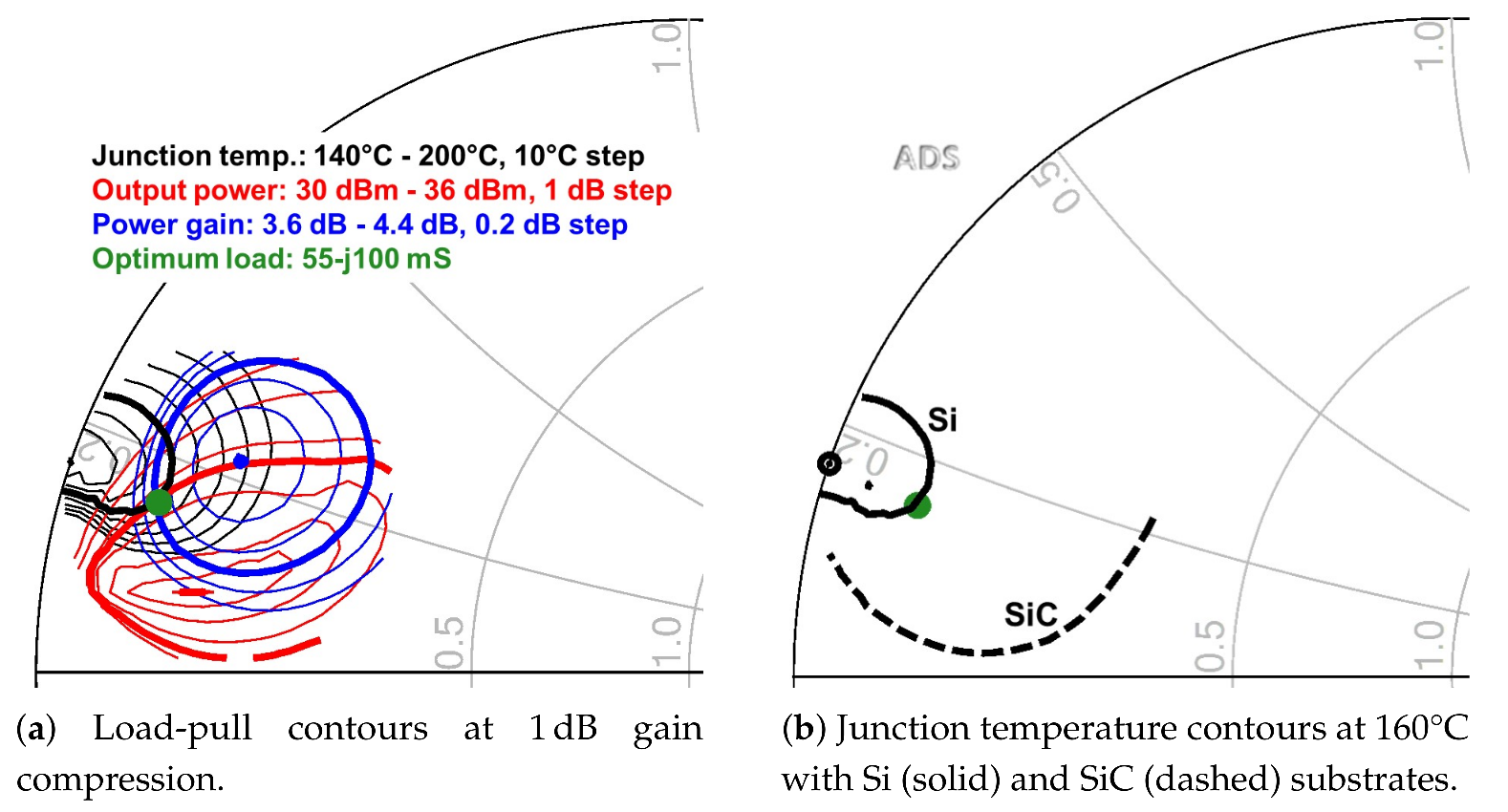
4.1.3. Load-Pull Analysis

Load-pull (LP) simulation results for the 8 × 75 μ m device at 36 GHz, at T BS = 80 ° C and at the selected bias point are shown in Figure 6a. Considering the high operating frequency and the stacked architecture, a tuned-load or a harmonic tuning approach is likely unfeasible, thus LP is performed assuming a constant load at all harmonics.
Adopting (12), thermal LP maps can be drawn. The 160 ° C limit on junction temperature (bold black contour) translates into a region of usable loads, where both output power and gain are lower than maximum. The absolute maximum output power is as high as 36 dBm but the corresponding load would lead to a junction temperature higher than 200 ° C. As can be noted in Figure 6b, the restrictions posed by thermal constraints on the choice of the optimum load is mainly related to the Si substrate. In fact, for the same dissipated power level, adopting the reference device thermal resistance for a SiC substrate in (12), the region of usable loads would be much more extended.
The optimum load can be found as the intersection of the maximum junction temperature contour with the highest possible output power and gain contours. Efficiency is not shown (to not overburden the plot) as it shows a very smooth variation around the selected load, which is 55 j 100 mS. The simulation results of the large-signal continuous wave (CW) power sweep with the selected optimum load are reported in Figure 7a. At the maximum PAE of 49%, the output power is 32.2 dBm, while associated gain and junction temperature are 4.5 dB and 155 ° C, respectively. The load seen at the intrinsic terminals (provided by the foundry model) as a function of the input power is shown in Figure 7b. The selected optimum value is effectively translated into an intrinsic load very close to the theoretical optimum resistance, which is around 37   Ω .

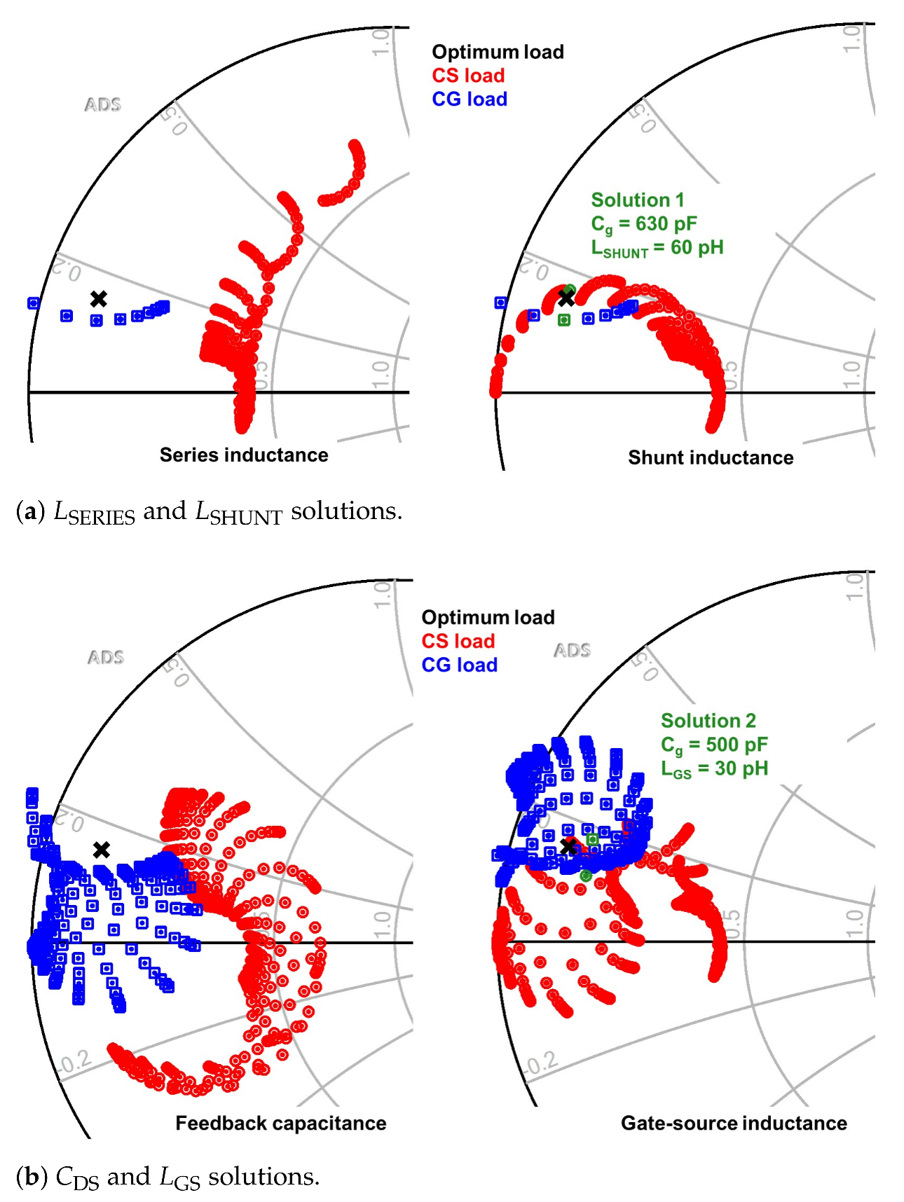
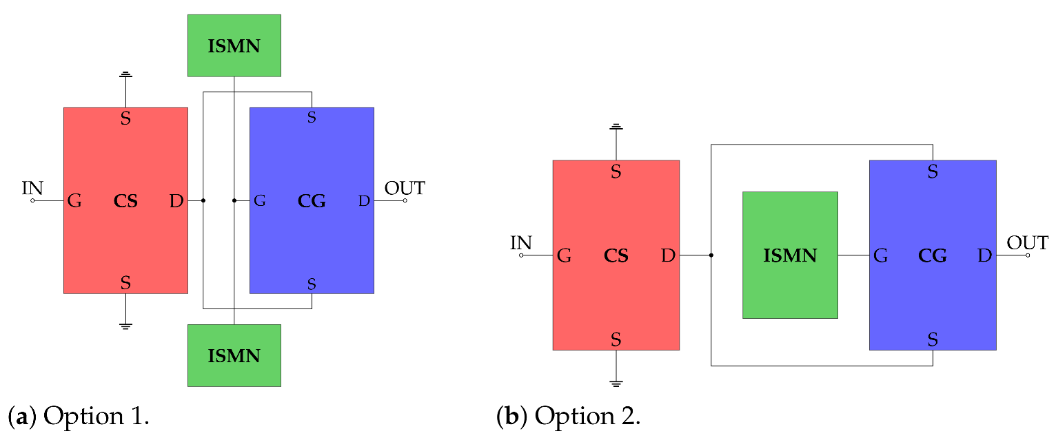
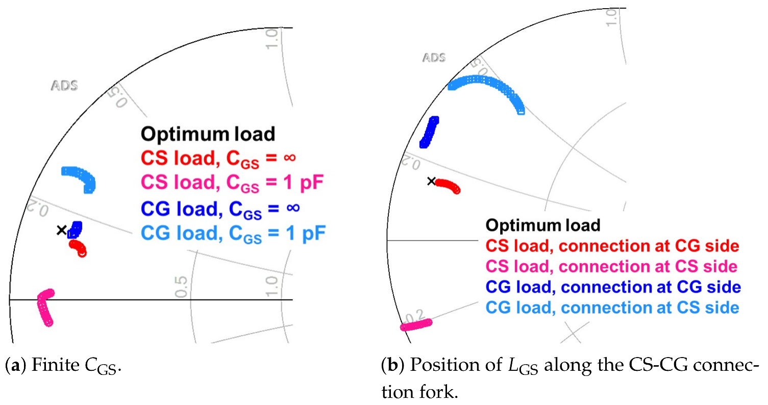
4.2. Stacked Inter-Stage Matching

At low frequency with respect to the cut-off, the optimum load is purely real and the CG input reactance due to C gs is low, therefore the gate capacitance C g alone can perform inter-stage matching. At high frequencies, instead, Z opt becomes complex, around ( 4 + j 7.5 )   Ω in the present case, and thus additional elements are needed.
The most widely adopted ISMNs are shown in Figure 8: series inductance ( L SERIES ) [10], feedback capacitance ( C DS ) [38], shunt inductance ( L SHUNT ) [43] and gate-source inductance ( L GS ) [22]. Even if other solutions may exist [27], only these four possibilities are considered in this design, since they only require one additional component beyond C g . Note that both devices’ loads depend on the external cell’s load Z L , which thus represents a further degree of freedom. However, for the sake of simplicity, in this design, we fixed Z L = 2 Z opt , which is the theoretical optimum value when both devices are individually perfectly matched.
Following a load-pull-like approach, Figure 9 shows the load seen by the two devices under concurrent sweep ( 10 16 to 10 11 ) of C g and each of the other matching elements. Figure 9a concerns the L SERIES and L SHUNT solutions, both not affecting the load of the CG stage, which is a function of C g only and for C g 630 pF it is as close as possible to Z opt . The series inductance moves the impedance seen by the CS stage along a constant resistance circle, without finding, in the present case, a good matching.
In a dual manner, the shunt inductance acts on the admittance seen by the CS stage, moving it along a constant conductance circle. With L SHUNT 60 pH, the best matching is also obtained for the CS stage, as highlighted in Figure 9a (green circle and square).
Figure 9b concerns instead the C DS and L GS solutions, which affect the load of both stages. Thanks to the Miller effect and the positive voltage gain of the CG stage, the feedback capacitance is translated into an equivalent negative capacitance at the input. A main feature of this solution is that it can compensate the gate power leakage [38]. As shown in Figure 10a, if the C DS value is chosen so as to draw a current equal to the gate current of the CG stage, a feedback power flow, equal and opposite to the leakage one, is created and the net CG source and drain currents become equal. In the present case, however, C DS is not a viable solution as it worsens the matching of the CG stage and at the same time cannot match the CS one.
Finally, the gate-source inductance modifies the equivalent value of the intrinsic C gs , being in parallel with it. As shown in Figure 10b, it can also compensate the gate power leakage by creating a controlled power flow P G toward the gate that provides an output power contribution that sums up in phase with P S and thus recovers the net power flow from CS drain to CG source. For the present case, the gate-source inductance represents a second possible solution. In particular, with C g 500 pF and L GS 30 pH, the best matching is achieved, as highlighted in Figure 9b (green circle and square).
Finally, Figure 11 shows the extrinsic and intrinsic loads seen by the two stages as a function of input power for the two identified solutions. At the intrinsic level, the L SHUNT solution achieves a very good match for the CS stage (better than 18 dB) while still keeping acceptable match (better than 8 dB) for the CG stage. For the L G S solution, instead, both stages are fairly well matched (better than 11 dB).

4.3. Layout Considerations

The most compact layout is that proposed in [24,43], where the drain of the CS stage is directly connected to the source of the CG one through air bridges. However, this solution presents two main drawbacks. First, it changes the original device layout, eliminating the drain (CS) and gate (CG) pads. However, the role of these pads is not negligible at 36 GHz, and cutting them out will worsen the accuracy of the device models. Secondly, air bridges are more lossy than micro-strip lines, can conduct only limited power, which can be an issue dealing with typical power levels of GaN, and may introduce cross-talk between the overlapping lines at the design frequency. We therefore chose to not modify the original device layout.
The active device model comes with two symmetrical source terminals, thus it is expected to be maximally accurate when used in a symmetrical layout. For the CS stage this means that via holes must be placed on both sides of the transistor, while for the CG stage this implies implementing a double-side access to the source terminals, with a C-shaped interconnection (fork). As shown in Figure 12, the ISMN elements can then be placed either outside or inside the fork. The first option ensures maximum cell compactness in the x-direction, but requires air bridges and ISMN splitting into two parallel networks placed at both sides of the cell to preserve symmetry, thus increasing the cell dimension along the y-direction. This architecture was selected for the L SHUNT solution, since in this case the power flowing toward the gate is expected to be small and thus sustainable by air bridges. For the L GS solution, instead, air bridges should be avoided, due to the non-negligible amount of power directed toward the gate. The second option was therefore adopted, yielding a cell more compact in the y-direction but larger in the x-direction. This implies the use of much longer interconnection lines, which can introduce a phase delay difficult, or even impossible, to be recovered with matching elements. On the other hand, it increases the distance between the transistors, and includes a via-hole in between, thus enhancing electro-magnetic and thermal decoupling.

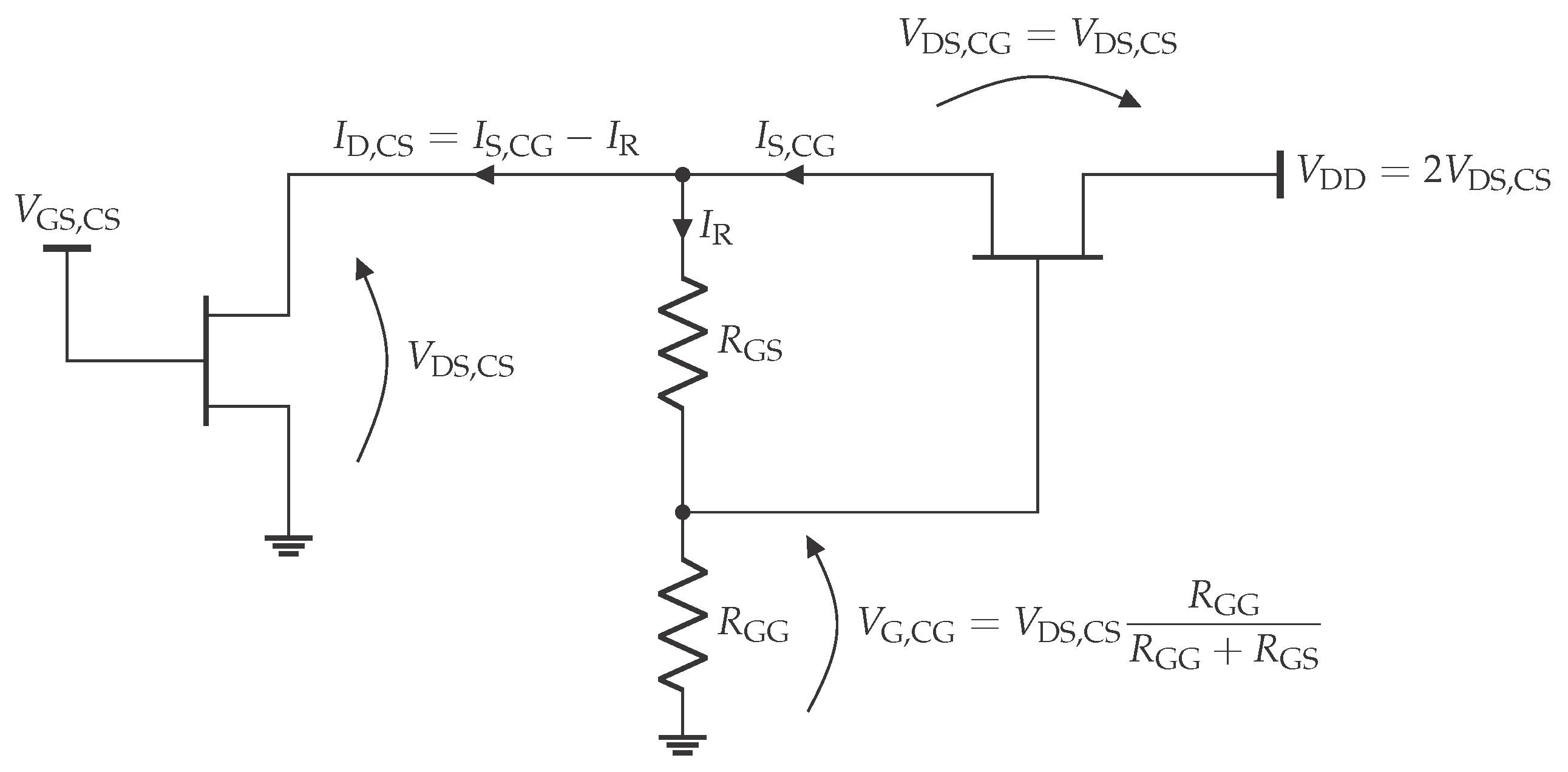
4.4. Self-Bias Network

Adopting a dedicated bias line for the CG gate voltage gives higher flexibility, and is often preferred when only one or two cells are adopted. However, for a PA exploiting more cells, the routing of these additional lines may become unsustainable and a self-bias approach should be preferred, where the gate-source voltage of the CG stage is derived by means of a resistive voltage divider from either the V D , CG = 22.5 V or V D , CS = V S , CG = 11.25 V. Looking at Figure 12, it is clear that the second option is much easier to be accommodated in the layout, and thus was selected, as shown in Figure 13.
To draw the same current of the CS stage, the CG stage must be biased at a voltage
V G , CG = V GS , CG + V DS , CS = V GS , CS + V DS , CS
In this design gate and drain voltages of the CS are −1.75 and 11.25 V, respectively, thus giving V G , CG = 9.5 V. Nevertheless, the assumption of equal drain-source DC voltages is valid only with no input power, or in small-signal conditions [12,27]. On the contrary, when the transistors are driven into compression, the DC components of the drain-source currents and consequently of the floating voltage V D , CS = V S , CG change. As shown in Figure 14a, this yields to early breakdown and early compression for the CS and CG stage, respectively. Since in a PA the cell works in non-linear regime, it is better to optimize the quiescent V G , CG for equal V DS close to saturation. Adopting a CG gate voltage lower than the nominal value unbalances the drain-source voltages in small-signal conditions, but makes them equal at the maximum output power, as shown in Figure 14b.

5. Circuit-Level (CL) Design

Figure 15 reports the circuit schematics of the two designed cells. All passive elements, except the gate capacitance of the L GS solution, are split into parallel pairs. Since via-holes are the most space-consuming components in a MMIC design, in both cells, all grounded elements share a common via-hole.
The selected technology provides metal-insulator-metal (MIM) capacitors with two different capacitance densities, namely 400 and 50 pF/ mm 2 . Considering also the size limits posed by the cell layout, the maximum achievable capacitance is limited to 1 pF, which cannot be considered an ideal short at the operating frequency, hence impacting on matching, as shown in Figure 16a, and requiring re-optimization.
As illustrated in Figure 16b, when distributed elements are used, not only their phase delay impacts on the loads seen by the devices, but also the choice of the connection point for the matching elements. Figure 16 concerns the L GS solution, but very similar considerations apply for the L SHUNT one.
The gate capacitances are implemented with lumped, low-capacitance-density MIM capacitors. The two shunt inductances are replaced by equivalent transmission lines, while squared spiral inductors are used for the gate-source inductances. Finally, self-bias resistances are replaced with GaN resistors (∼400 Ω / ). The value of the final optimized components is reported in Table 2.
Both cells achieve, at 36 GHz, more than 3 W of output power with saturated power gain and efficiencies above 7.2 dB and 40%, respectively, as shown in Figure 17a. The achieved DC voltage distribution is also very good, as shown in Figure 17b.

6. Electro-Magnetic (EM) Design

In Figure 18, the final layouts of the two cells are reported. To achieve cell compactness, elements are very close to each other, thus extensive EM optimization is required to account for EM coupling effects.

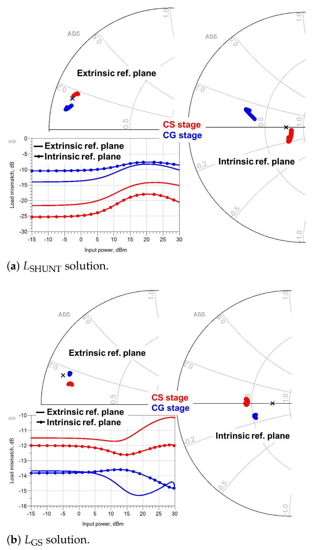
6.1. EM Simulation Results for the Shunt-Inductance-Based Cell

Figure 19 shows the simulated results of the L SHUNT -based cell. The ISMN proved not to be able to provide the device matching required and therefore the achieved performance was sensibly lower than the CL predictions in terms of output power (below 1 W), gain (even below 0 dB in small-signal) and PAE (below 10%). As discussed in [37], these results can be ascribed to actual cross-talk in the ISMN structure, as detailed in Figure 20 reporting the EM-simulated RF current density distribution. The air-bridge crossing, the proximity of C g and C SHUNT capacitances and via sharing among them, result in creating an undesired path between the gate and the source of the CG stage (highlighted with dashed circles). In particular, even if this is not the actual operating condition of the cell, if we observe the current distribution obtained when injecting power from the gate of the CG device (right plot), rather big cross-talk currents are found to flow in L SHUNT , which should be instead isolated from the gate of the CG stage (see Figure 15a).
The gate-source cross-talk proved to be almost unavoidable in a compact cell. Thus, even if possible improvements may have been achieved, the L SHUNT -based cell was discarded in favor of the L GS -based one, where the gate-source coupling is part of the ISMN itself and thus it can be carefully EM-designed.

6.2. EM Simulation Results for the Gate-Source-Inductance-Based Cell

Figure 21 shows the results obtained after EM optimization of the L GS -based cell. The EM-simulated performance is very close to the circuit-level one. Saturated output power is around 3 W in moderate compression, with an associated gain in excess of 7 dB. The maximum PAE is around 40%, only a few percentage points below CL predictions. Compared to the CS stage alone, there is clearly a gain/power enhancement while PAE remains reasonably high. The actual loads seen by the devices are close to the optimum value, and the obtained voltage and current waveforms, as shown in Figure 22 for all swept power levels, are rather good, in terms of both phase alignment and magnitude equalization.
Figure 23 shows how the CS output power is split almost equally between the source and gate of the CG stage through the two L GS inductors, which carry the highest RF currents densities.
Figure 24a confirms the gain boost effect of device stacking: the gain of the CS alone is below 5 dB, in line with Figure 7a, while the CG contribution is between 2 and 3 dB, so that the total gain is raised up to a maximum of 7.6 dB. The ISMN losses are bounded between 0.5 and 0.6 dB. Due to the very deep Class AB bias point selected, the power gain expands more than 3 dB when increasing the input power.
Finally, Figure 24b shows the DC drain-source voltages obtained at EM level, compared to the CL results, demonstrating that proper voltage distribution is maintained.

7. Stability, Linearity and Thermal Assessment

To conclude cell assessment, this section reports the stability, linearity and thermal analyses on the EM-based L GS -based solution.

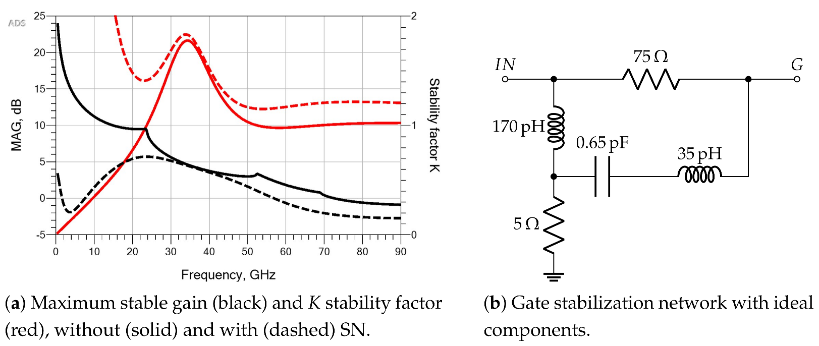
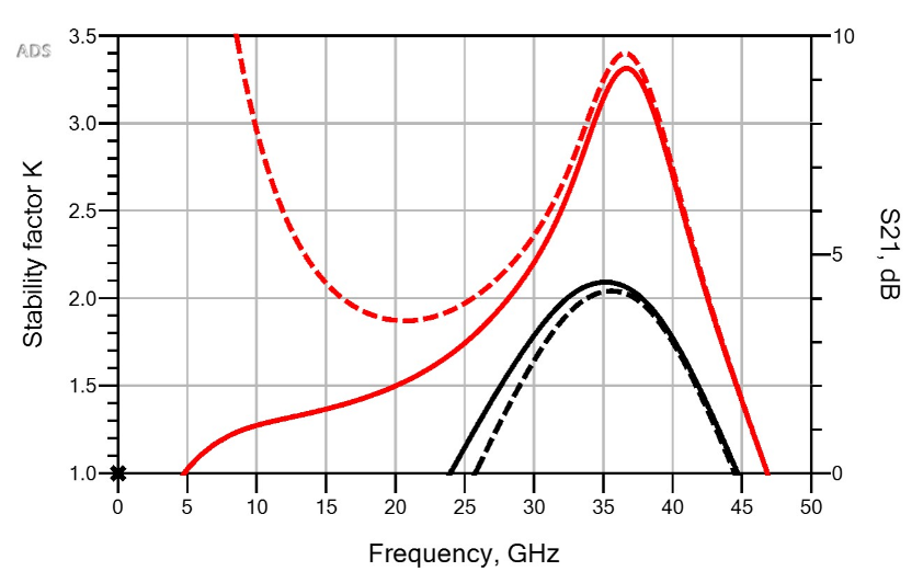
7.1. Stability Analysis

The cell small-signal stability can be investigated by means of the classical Rollett’s stability factor K, since, as opposite to parallel combination, series combination does not create any even/odd-mode internal loop impairing stability. As shown in Figure 25, the cell is unconditionally stable from 5 GHz to more than 45 GHz, where gain falls below 0 dB. At low frequency, unconditional stability can be achieved with the same SN adopted for the CS device alone (Figure 5b) with negligible gain reduction at 36 GHz.

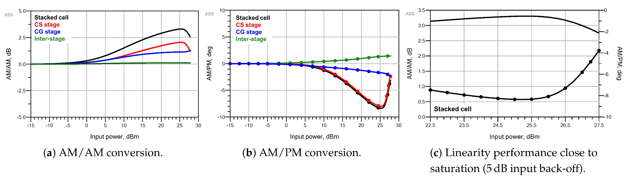
7.2. Linearity Analysis

The cell has not been optimized for linearity. However, it is interesting to assess the final linearity performance achieved. In narrow-band design, the AM/AM and AM/PM curves are the most significant figures of merit. The results on the EM-optimized cell are reported in Figure 26. The maximum AM/AM (Figure 26a) is 3.5 dB, due to the sensible gain expansion expected from the selected bias point, very close to pinch-off. However, as highlighted in Figure 26c, close to saturation the gain variation is within 0.4 dB.
AM/PM conversion (Figure 26b) is dominated by the CS stage, being the phase distortion introduced by the CG stage almost totally compensated by the ISMN. The maximum value is around 8 ° , which is a reasonable value, while close to saturation the range of phase variation is about 4 ° (Figure 26c).

7.3. Thermal Analysis

As anticipated in Section 3.1, junction temperature is kept under control during the design phase by means of a simplified model starting form the simulated CW dissipated power. As demonstrated in Figure 27a, after EM optimization, it remains below 160 ° C for all input power levels.
Finally, 3D-FEM thermal simulation results of the entire cell, at isothermal 80 ° C MMIC back-side temperature, are shown in Figure 27b. The highest temperature is 144 ° C, well below the maximum limit for space applications, and it is recorded at the inmost gate fingers of the CG device. As can be noted, the two devices undergo similar thermal stress and cross-heating is very small thanks to the heat-sink effect of the via hole in between, which lowers the temperature down to a minimum of 84.3 ° C.

8. Conclusions

In this contribution, the design of a stacked cell in GaN-on-Si technology for Ka-band space applications is detailed. Starting from the basic concepts, the limiting factors of the stacked configuration when pursued for a high frequency operating range are discussed together with the constraints imposed by thermal reliability. The designs of two stacked cells are presented and compared, highlighting the impact of electro-magnetic and thermal cross-talk effects.

Author Contributions

Conceptualization, review and editing, all authors; original draft preparation, C.R.; investigation and formal analysis, C.R. and M.P.; supervision, C.F. and P.C.; project administration, P.C. All authors have read and agreed to the published version of the manuscript.

Funding

This research was funded by ESA within the project Ka-band HPA MMIC for CS2-FO under the Earth Observation Envelope Programme EOEP-5 Block 1.

Acknowledgments

Iain Davies from ESA-ESTEC is warmly acknowledged for the useful discussion.

Conflicts of Interest

The authors declare no conflict of interest.

References

  1. Chen, S.; Nayak, S.; Campbell, C.; Reese, E. High Efficiency 5 W/10 W 32–38 GHz Power Amplifier MMICs Utilizing Advanced 0.15 μm GaN HEMT Technology. In Proceedings of the 2016 IEEE Compound Semiconductor Integrated Circuit Symposium (CSICS), Austin, TX, USA, 23–26 October 2016; pp. 1–4. [Google Scholar] [CrossRef]
  2. Moron, J.; Leblanc, R.; Lecourt, F.; Frijlink, P. 12 W, 30% PAE, 40 GHz power amplifier MMIC using a commercially available GaN/Si process. In Proceedings of the 2018 IEEE/MTT-S International Microwave Symposium-IMS, Philadelphia, PA, USA, 10–15 June 2018; pp. 1457–1460. [Google Scholar] [CrossRef]
  3. Estella, N.; Camargo, E.; Schellenberg, J.; Bui, L. High-Efficiency, Ka-band GaN Power Amplifiers. In Proceedings of the 2019 IEEE MTT-S International Microwave Symposium (IMS), Boston, MA, USA, 2–7 June 2019; pp. 568–571. [Google Scholar] [CrossRef]
  4. Cidronali, A.; Passafiume, M.; Colantonio, P.; Collodi, G.; Florian, C.; Leuzzi, G.; Pirola, M.; Ramella, C.; Santarelli, A.; Traverso, P. System Level Analysis of Millimetre-wave GaN-based MIMO Radar for Detection of Micro Unmanned Aerial Vehicles. In Proceedings of the 2019 PhotonIcs & Electromagnetics Research Symposium-Spring (PIERS-Spring), Rome, Italy, 17–20 June 2019; pp. 438–450. [Google Scholar] [CrossRef]
  5. Ramella, C.; Florian, C.; Cipriani, E.; Pirola, M.; Giannini, F.; Colantonio, P. Ka-band 4 W GaN/Si MMIC power amplifier for CW radar applications. In Proceedings of the 2020 15th European Microwave Integrated Circuits Conference (EuMIC), Utrecht, The Netherlands, 10–15 January 2021; pp. 33–36. [Google Scholar] [CrossRef]
  6. Colantonio, P.; Giannini, F.; Limiti, E. High Efficiency RF and Microwave Solid State Power Amplifiers; Microwave and Optical Engineering; Wiley: New York, NY, USA, 2009. [Google Scholar]
  7. European Cooperation for Space Standardization. ECSS-Q-ST-30-11C Rev 1—Space Product Assurance—Derating EEE Components; European Cooperation for Space Standardization: Noordwijk, The Netherlands, 2011. [Google Scholar]
  8. European Space Agency. GaN Reliability Enhancement and Technology Transfer Initiative (GREAT2); European Space Agency/European Space Technology and Research Centre: Noordwijk, The Netherlands, 2008. [Google Scholar]
  9. Ramella, C.; Pirola, M.; Reale, A.; Ramundo, M.; Colantonio, P.; Maur, M.A.D.; Camarchia, V.; Piacibello, A.; Giofrè, R. Thermal-aware GaN/Si MMIC design for space applications. In Proceedings of the 2019 IEEE International Conference on Microwaves, Antennas, Communications and Electronic Systems (COMCAS), Tel-Aviv, Israel, 4–6 November 2019; pp. 1–6. [Google Scholar]
  10. Shifrin, M.; Ayasli, Y.; Katzin, P. A new power amplifier topology with series biasing and power combining of transistors. In Proceedings of the IEEE 1992 Microwave and Millimeter-Wave Monolithic Circuits Symposium Digest of Papers, Albuquerque, NM, USA, 1–3 June 1992; pp. 39–41. [Google Scholar] [CrossRef]
  11. Dabag, H.; Hanafi, B.; Golcuk, F.; Agah, A.; Buckwalter, J.F.; Asbeck, P.M. Analysis and Design of Stacked-FET Millimeter-Wave Power Amplifiers. IEEE Trans. Microw. Theory Tech. 2013, 61, 1543–1556. [Google Scholar] [CrossRef]
  12. Pornpromlikit, S.; Jeong, J.; Presti, C.D.; Scuderi, A.; Asbeck, P.M. A Watt-Level Stacked-FET Linear Power Amplifier in Silicon-on-Insulator CMOS. IEEE Trans. Microw. Theory Tech. 2010, 58, 57–64. [Google Scholar] [CrossRef]
  13. Kim, J.; Dabag, H.; Asbeck, P.; Buckwalter, J.F. Q-Band and W-Band Power Amplifiers in 45-nm CMOS SOI. IEEE Trans. Microw. Theory Tech. 2012, 60, 1870–1877. [Google Scholar] [CrossRef]
  14. Oßmann, P.; Fuhrmann, J.; Dufrêne, K.; Fritzin, J.; Moreira, J.; Pretl, H.; Springer, A. Design of a Fully Integrated Two-Stage Watt-Level Power Amplifier Using 28-nm CMOS Technology. IEEE Trans. Microw. Theory Tech. 2016, 64, 188–199. [Google Scholar] [CrossRef]
  15. Zhang, C.; Li, Z.; Cheng, G.; Wang, H.; Li, Z. A 26.5–40 GHz Stacked Power Amplifier in 130 nm SiGe BiCMOS Technology. In Proceedings of the 2018 IEEE International Conference on Integrated Circuits, Technologies and Applications (ICTA), Beijing, China, 21–23 November 2018; pp. 36–37. [Google Scholar] [CrossRef]
  16. Aikio, J.P.; Hietanen, M.; Tervo, N.; Rahkonen, T.; Pärssinen, A. Ka-Band 3-Stack Power Amplifier with 18.8 dBm Psat and 23.4% PAE Using 22nm CMOS FDSOI Technology. In Proceedings of the 2019 IEEE Topical Conference on RF/Microwave Power Amplifiers for Radio and Wireless Applications (PAWR), Orlando, FL, USA, 20–23 January 2019; pp. 1–3. [Google Scholar] [CrossRef] [Green Version]
  17. Mohammadi, S.; Shan, H.; Conrad, N.; Hathorn, S.; Peterson, J. High-Efficiency Stacked Cell CMOS SOI Power Amplifiers for 5G Applications. In Proceedings of the 2019 IEEE MTT-S International Microwave Conference on Hardware and Systems for 5G and Beyond (IMC-5G), Atlanta, GA, USA, 15–16 August 2019; pp. 1–4. [Google Scholar] [CrossRef]
  18. Chang, Y.; Lu, B.; Wang, Y.; Wang, H. A Ka-Band Stacked Power Amplifier with 24.8-dBm Output Power and 24.3% PAE in 65-nm CMOS Technology. In Proceedings of the 2019 IEEE MTT-S International Microwave Symposium (IMS), Boston, MA, USA, 2–7 June 2019; pp. 316–319. [Google Scholar] [CrossRef]
  19. Inoue, A.; Goto, S.; Kunii, T.; Ishikawa, T.; Matsuda, Y. A high efficiency, high voltage, balanced cascode FET. In Proceedings of the IEEE MTT-S International Microwave Symposium Digest 2005, Long Beach, CA, USA, 17 June 2005; pp. 4–672. [Google Scholar] [CrossRef]
  20. Lee, C.; Kim, Y.; Koh, Y.; Kim, J.; Seo, K.; Jeong, J.; Kwon, Y. A 18 GHz Broadband Stacked FET Power Amplifier Using 130 nm Metamorphic HEMTs. IEEE Microw. Wirel. Compon. Lett. 2009, 19, 828–830. [Google Scholar] [CrossRef]
  21. Park, Y.; Kim, Y.; Choi, W.; Woo, J.; Kwon, Y. X-to-K band broadband watt-level power amplifier using stacked-FET unit cells. In Proceedings of the 2011 IEEE Radio Frequency Integrated Circuits Symposium, Baltimore, MD, USA, 5–7 June 2011; pp. 1–4. [Google Scholar] [CrossRef]
  22. Kim, Y.; Kwon, Y. Analysis and Design of Millimeter-Wave Power Amplifier Using Stacked-FET Structure. IEEE Trans. Microw. Theory Tech. 2015, 63, 691–702. [Google Scholar] [CrossRef]
  23. Nguyen, D.P.; Pham, A. An Ultra Compact Watt-Level Ka-Band Stacked-FET Power Amplifier. IEEE Microw. Wirel. Components Lett. 2016, 26, 516–518. [Google Scholar] [CrossRef] [Green Version]
  24. Ramella, C.; Piacibello, A.; Camarchia, V.; Pirola, M.; Quaglia, R. Characterization-oriented design of a compact GaAs MMIC 3-stacked power cell. In Proceedings of the 2016 2016 21st International Conference on Microwave, Radar and Wireless Communications (MIKON), Krakow, Poland, 9–11 May 2016; pp. 1–4. [Google Scholar] [CrossRef]
  25. Piacibello, A.; Pirola, M.; Camarchia, V.; Ramella, C.; Quaglia, R. A Ku-band Compact MMIC PA based on Stacked GaAs pHEMT cells. In Proceedings of the 2018 International Workshop on Integrated Nonlinear Microwave and Millimetre-wave Circuits (INMMIC), Brive La Gaillarde, France, 5–6 July 2018; pp. 1–3. [Google Scholar] [CrossRef]
  26. Thome, F.; Leuther, A.; Schlechtweg, M.; Ambacher, O. Broadband High-Power W-Band Amplifier MMICs Based on Stacked-HEMT Unit Cells. IEEE Trans. Microw. Theory Tech. 2018, 66, 1312–1318. [Google Scholar] [CrossRef]
  27. van der Bent, G.; de Hek, P.; van Vliet, F.E. Design Procedure for Integrated Microwave GaAs Stacked-FET High-Power Amplifiers. IEEE Trans. Microw. Theory Tech. 2019, 67, 3716–3731. [Google Scholar] [CrossRef]
  28. Ezzeddine, B.A.; Hung, H.A.; Viveiros, E.; Huang, H. High-power GaN MMIC PA Over 40–4000 MHz. In Proceedings of the 2013 IEEE MTT-S International Microwave Symposium Digest (MTT), Seattle, WA, USA, 2–7 June 2013; pp. 1–4. [Google Scholar] [CrossRef]
  29. Martin, A.; Reveyrand, T.; Campovecchio, M.; Aubry, R.; Piotrowicz, S.; Floriot, D.; Quere, R. Design of GaN-based balanced cascode cells for wide-band distributed power amplifier. In Proceedings of the 2007 European Microwave Integrated Circuit Conference, Munich, Germany, 8–10 October 2007; pp. 154–157. [Google Scholar] [CrossRef] [Green Version]
  30. Costanzo, F.; Giofrè, R.; Camarchia, V.; Colantonio, P.; Limiti, E. A Ka-band Doherty Power Amplifier using an innovative Stacked-FET Cell. In Proceedings of the 2019 15th Conference on Ph.D Research in Microelectronics and Electronics (PRIME), Lausanne, Switzerland, 15–18 July 2019; pp. 165–168. [Google Scholar] [CrossRef]
  31. Ramella, C.; Pirola, M.; Colantonio, P. A Ka-band 33 dBm Stacked Power Amplifier Cell in 100 nm GaN-on-Si Technology. In Proceedings of the 2020 23rd International Microwave and Radar Conference (MIKON), Warsaw, Poland, 5–8 October 2020; pp. 204–208. [Google Scholar] [CrossRef]
  32. Sun, W.; Kuo, C. A 19.1% PAE, 22.4-dBm 53-GHz Parallel Power Combining Power Amplifier with Stacked-FET Techniques in 90-nm CMOS. In Proceedings of the 2019 IEEE MTT-S International Microwave Symposium (IMS), Boston, MA, USA, 2–7 June 2019; pp. 327–330. [Google Scholar] [CrossRef]
  33. Li, S.; Fritsche, D.; Carta, C.; Ellinger, F. Design and characterization of a 12–40 GHz power amplifier in SiGe technology. In Proceedings of the 2018 IEEE Topical Conference on RF/Microwave Power Amplifiers for Radio and Wireless Applications (PAWR), Anaheim, CA, USA, 14–17 January 2018; pp. 23–25. [Google Scholar] [CrossRef]
  34. Jayamon, J.; Gurbuz, O.; Hanafi, B.; Agah, A.; Buckwalter, J.; Rebeiz, G.; Asbeck, P. Spatially power-combined W-band power amplifier using stacked CMOS. In Proceedings of the 2014 IEEE Radio Frequency Integrated Circuits Symposium, Tampa, FL, USA, 1–3 June 2014; pp. 151–154. [Google Scholar] [CrossRef]
  35. Nguyen, D.P.; Pham, T.; Pham, A. A 28-GHz Symmetrical Doherty Power Amplifier Using Stacked-FET Cells. IEEE Trans. Microw. Theory Tech. 2018, 66, 2628–2637. [Google Scholar] [CrossRef]
  36. Ezzeddine, A.K.; Huang, H.C. The high voltage/high power FET (HiVP). In Proceedings of the IEEE Radio Frequency Integrated Circuits (RFIC) Symposium 2003, Philadelphia, PA, USA, 9–10 June 2003; pp. 215–218. [Google Scholar] [CrossRef]
  37. Ramella, C.; Piacibello, A.; Camarchia, V.; Pirola, M. Electro-magnetic Crosstalk Effects in a Millimeter-wave MMIC Stacked Cell. In Proceedings of the 2020 International Workshop on Integrated Nonlinear Microwave and Millimetre-Wave Circuits (INMMiC), Cardiff, UK, 16–17 July 2020; pp. 1–3. [Google Scholar] [CrossRef]
  38. Ezzeddine, A.K.; Huang, H.C.; Singer, J.L. UHiFET—A new high-frequency High-Voltage device. In Proceedings of the 2011 IEEE MTT-S International Microwave Symposium, Baltimore, MD, USA, 5–10 June 2011; p. 1. [Google Scholar] [CrossRef]
  39. Berroth, M.; Bosch, R. Broad-band determination of the FET small-signal equivalent circuit. IEEE Trans. Microw. Theory Tech. 1990, 38, 891–895. [Google Scholar] [CrossRef] [Green Version]
  40. Thome, F.; Maroldt, S.; Ambacher, O. Prospects and Limitations of Stacked-FET Approaches for Enhanced Output Power in Voltage-Controlled Oscillators. IEEE Trans. Microw. Theory Tech. 2016, 64, 836–846. [Google Scholar] [CrossRef]
  41. Gasmi, A.; El Kaamouchi, M.; Poulain, J.; Wroblewski, B.; Lecourt, F.; Dagher, G.; Frijlink, P.; Leblanc, R. 10W power amplifier and 3W transmit/receive module with 3 dB NF in Ka band using a 100 nm GaN/Si process. In Proceedings of the 2017 IEEE Compound Semiconductor Integrated Circuit Symposium (CSICS), Miami, FL, USA, 22–25 October 2017; pp. 1–4. [Google Scholar] [CrossRef]
  42. OMMIC. U-GaN Design Manual V1.2.4; OMMIC: Limeil-Brévannes, France, 2018. [Google Scholar]
  43. Fersch, T.; Quaglia, R.; Pirola, M.; Camarchia, V.; Ramella, C.; Khoshkholgh, A.J.; Ghione, G.; Weigel, R. Stacked GaAs pHEMTs: Design of a K-band power amplifier and experimental characterization of mismatch effects. In Proceedings of the 2015 IEEE MTT-S International Microwave Symposium, Phoenix, AZ, USA, 17–22 May 2015; pp. 1–4. [Google Scholar] [CrossRef]
Figure 1. N-device stacked PA with highlighted device matching condition (red, dashed) and gate power leakage (blue).
Electronics 10 01784 g001
Figure 2. Simplified intrinsic equivalent of the nth CG stage.
Electronics 10 01784 g002
Figure 3. R th , REF extraction from 3D thermal simulations as a function of back-side temperature and junction temperature.
Electronics 10 01784 g003
Figure 4. DC characteristics of the 8 × 75 μ m device (black) at T BS = 80 ° C and selected bias point (red dot).
Electronics 10 01784 g004
Figure 5. Small-signal stability analysis of the 8 × 75 μ m device at T BS = 80 ° C and at the selected bias point.
Electronics 10 01784 g005
Figure 6. Load-pull simulation results of the 8 × 75 μ m device at 36 GHz, with T BS = 80 ° C and at the selected bias point.
Electronics 10 01784 g006
Figure 7. Large-signal simulation results of the 8 × 75 μ m device at 36 GHz, with T BS = 80 ° C and at the selected bias point.
Electronics 10 01784 g007
Figure 8. Most widely adopted inter-stage matching networks: series inductance (cyan), shunt inductance (blue), feedback capacitance (green) and gate-source inductance (red).
Electronics 10 01784 g008
Figure 9. Load of CS (red circles) and CG (blue squares) stages as a function of ISMN components compared to Z opt (black cross).
Electronics 10 01784 g009
Figure 10. Gate power leakage compensation.
Electronics 10 01784 g010
Figure 11. Load of CS (red) and CG (blue) stages as a function of input power.
Electronics 10 01784 g011
Figure 12. Possible symmetrical cell layouts.
Electronics 10 01784 g012
Figure 13. Adopted self-bias network (stacked cell in DC operation).
Electronics 10 01784 g013
Figure 14. DC drain-source voltages of the CS (red) and CG (blue) stage as a function of input power for both L SHUNT -based (circles) and L GS -based (crosses) solutions.
Electronics 10 01784 g014
Figure 15. Layout-like schematics of the cells (transmission lines not shown).
Electronics 10 01784 g015
Figure 16. Effect of on matching of CL non-idealities.
Electronics 10 01784 g016
Figure 17. Optimized circuit-level performance of the L SHUNT -based (circles) and L GS -based (crosses) cells at 36 GHz.
Electronics 10 01784 g017
Figure 18. Layout of the two designed cells.
Electronics 10 01784 g018
Figure 19. Comparison between CL and EM simulations for the L SHUNT cell.
Electronics 10 01784 g019
Figure 20. EM-simulated current densities in the L SHUNT cell. Blue to red means lowest to highest current density.
Electronics 10 01784 g020
Figure 21. Comparison between CL and EM simulations for the L GS cell.
Electronics 10 01784 g021
Figure 22. EM-simulated time-domain waveforms of the L GS cell.
Electronics 10 01784 g022
Figure 23. Power split between gate and source in the L GS cell.
Electronics 10 01784 g023
Figure 24. EM simulation results of the L GS solution.
Electronics 10 01784 g024
Figure 25. Stability factor K (red) and S 21 (black) of the cell without (solid) and with (dashed) the SN of Figure 5b.
Electronics 10 01784 g025
Figure 26. AM/AM (no symbols) and AM/PM (circles) simulations at 36 GHz of the L GS -based cell and its sub-stages.
Electronics 10 01784 g026
Figure 27. Thermal simulations of the L GS cell.
Electronics 10 01784 g027
Table 1. Features of the OMMIC D01GH GaN-on-Si process.
FeatureValue
Cut-off frequency f t > 90 GHz *
Saturation current I DSS > 850 mA/mm *
Threshold voltage V TH 2 V *
Output power P out > 2.9 W/mm *
Junction temperature T j 200   ° C *
Breakdown voltage V BD >50 V  
Quiescent V DS 15 V  
* simulated;   from manual.
Table 2. Circuit level component values of the designed stacked cells.
ComponentValue L SHUNT SolutionValue L GS Solution
C g 165 fF (MIM)175 fF (MIM)
L SHUNT / L GS 92.5 pH (transmission lines)170 pH (spiral inductors)
C SHUNT / C GS 0.9 pF (MIM)0.8 pF (MIM)
R GS 1140  Ω 1320  Ω
R GG 4400  Ω 6500  Ω
Publisher’s Note: MDPI stays neutral with regard to jurisdictional claims in published maps and institutional affiliations.

