Article

Active Gate Driver and Management of the Switching Speed of GaN Transistors during Turn-On and Turn-Off

1
Ecole Centrale Lyon, Ampère-CNRS UMR5005, Université Claude Bernard Lyon 1, F-69621 Villeurbanne, France
2
Institut Interdisciplinaire d’Innovation Technologique, Université de Sherbrooke, Sherbrooke, QC J1K 2R1, Canada
3
HYBRIA Institute of Business and Technologies, INSA Lyon, Ampère-CNRS, Université de Lyon, F-69621 Vil-leurbanne, France
4
Arts et Metiers Institute of Technology, Université de Lille, Centrale Lille, Junia, ULR 2697, Laboratoire d’Electrotechnique et d’Electronique de Puissance, F-59000 Lille, France
*
Author to whom correspondence should be addressed.
Electronics 2021, 10(2), 106; https://doi.org/10.3390/electronics10020106
Submission received: 16 November 2020 / Revised: 24 December 2020 / Accepted: 26 December 2020 / Published: 7 January 2021
(This article belongs to the Special Issue Innovative Technologies in Power Converters)

Abstract

:
The paper investigates the management of drain voltage and current slew rates (i.e., dv/dt and di/dt) of high-speed GaN-based power switches during the transitions. An active gate voltage control (AGVC) is considered for improving the safe operation of a switching cell. In an application of open-loop AGVC, the switching speeds vary significantly with the operating point of the GaN HEMT on either or both current and temperature. A closed-loop AGVC is proposed to operate the switches at a constant speed over different operating points. In order to evaluate the reduction in the electromagnetic disturbances, the common mode currents in the system were compared using the active and a standard gate voltage control (SGVC). The closed-loop analysis carried out in this paper has shown that discrete component-based design can introduce limitations to fully resolve the problem of high switching speeds. To ensure effective control of the switching operations, a response time fewer than 10 ns is required for this uncomplex closed-loop technique despite an increase in switching losses.

1. Introduction

Very high frequency operation capabilities of wide band-gap semiconductor devices (such as GaN and SiC) made them good candidates for high efficiency of static converter [1,2,3,4,5]. However, the safe operation of the devices in converters degrades during very fast transitions of both current and voltage [6,7,8]. Most commonly, passive control techniques are used in managing transitions [9,10,11,12,13,14]. The methods applied in passive control adjust either/or both the gate resistance and the parasitic gate capacitance of a transistor. One of the main disadvantages of passive control is a lack of compensation against the variations of the current and voltage parameters of the converter, which, therefore, increase switching losses. An open-loop passive control technique is presented in References [15,16,17] to mitigate this issue. In this technique, the switching process has been divided into several sequences while introducing a passive element for each sequence. Compared to the basic methods, this open-loop method reduces the losses. However, additional losses remain significant since the open-loop passive controls are unable to compensate for the variation in the converter parameters.
A closed-loop active driver for silicon-based IGBTs (Insulate Gate Bipolar Transistor) and MOSFETs (Metal Oxide Semiconductor Field Effect Transistor) has been proposed in References [17,18,19,20]. The active driver circuit in Reference [19] presented the current transient (di/dt) control of an IGBT, based on a 50-nH common parasitic inductance between the power and the control paths. For GaN-based designs, the introduction of such a parasitic value is unacceptable as the parasitic transients can damage the device during fast transitions. An active closed-loop control based on a capacitor lower than 20 nF has been proposed for a GaN HEMT (High Electron Mobility Transistor) in References [21,22]. However, this technique under-utilized the fast switching capability of the GaN HEMTs as it used a switching speed lower than that of an Si-based MOSFET or IGBT.
In all those GaN transistor-based solutions, discrete components and complex circuits were used to solve the issue of high-speed switches. In this paper, we are proposing a less complex closed-loop to manage potential limits of switching speed. The evaluation of this discrete component-based circuit can be used to determine the response time, switching speed, and the losses. Furthermore, we determined the limitations of the AGVC (Active Gate Voltage Control) technique built using a discrete component to control switching speed of a GaN HEMT.
Firstly, a study of an analysis of active gate drive techniques for GaN power transistors is summarized. The mathematical analysis for switching speeds is discussed in Section 2. Section 4 details a proposal of an open-loop active gate voltage control (AGVC) technique. By addressing the issues in the open-loop approach, a new closed-loop control technique is introduced in Section 5. Finally, Section 6 concludes by summarizing the findings.

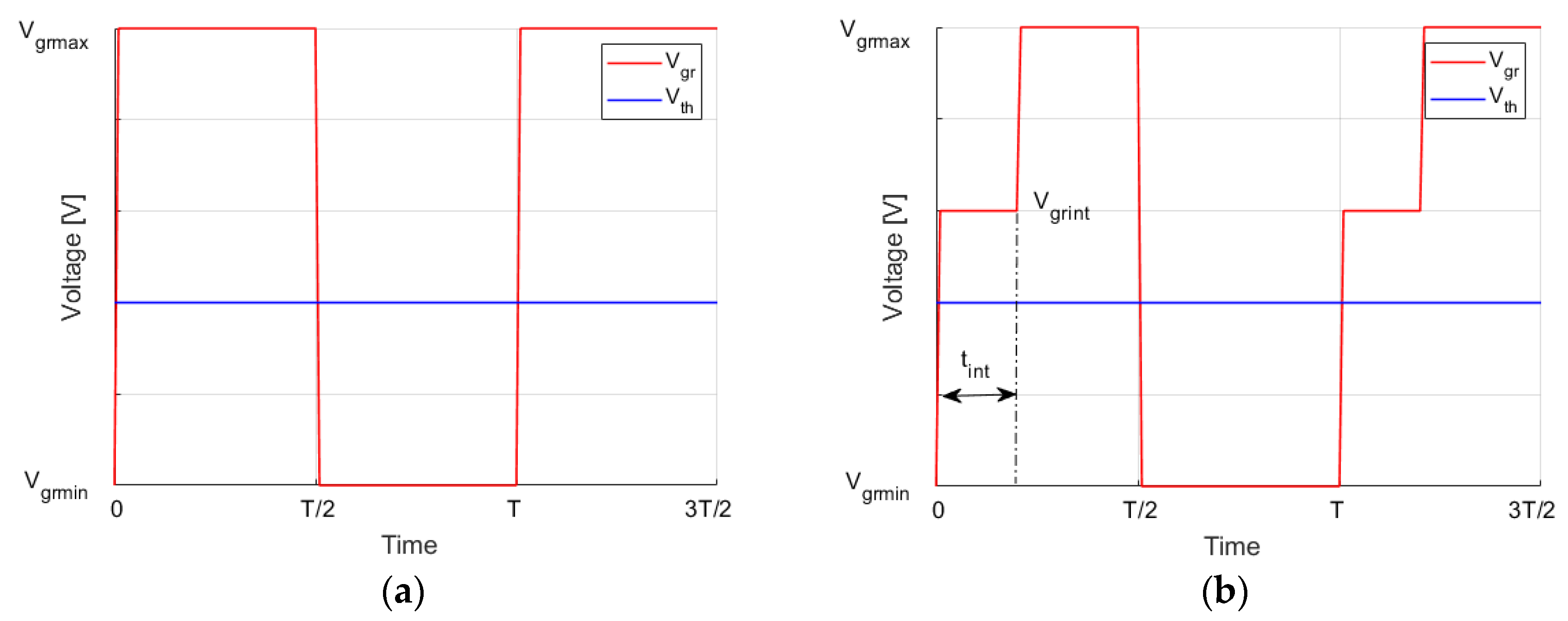
2. Open-Loop Active Gate Voltage Control during Turn-On

Figure 1 illustrates a schematic diagram of a simple switching cell in a buck configuration. The fluctuations in drain voltage and current slew rates (dv/dt and di/dt) are due to the fast switching operation of the converter. GaN-based switch designs are more sensitive to these fluctuations. Besides, they depend on (i) the transistor parameters: threshold voltage (Vth), gate-drain capacitance ( C gd ), gate-source capacitance ( C gs ), and the gain ( g m ), (ii) the characteristics of the driver: output voltage ( V gr ) and gate current ( I g ) of the driver, and (iii) passive elements of the gate control circuit ( R g and L S ) [20,21,22]. The transition current during turn-on of the GaN transistor is given by Equation (1):
di d , on dt = g m ( V grmax V th ) R g ( C gd C gs ) + g m · L S
The reduction in the switching speed can be carried out by two methods: passive or active control of the gate drive. In general, the passive method is achieved by adjusting the passive elements of the driver loop (Rg or and Cgd). The high losses generated by these elements are one of the drawbacks that make the passive control method less interesting. The active control method is achieved by adjusting the electrical parameters of the driver such as the maximum gate supply voltage (Vgrmax) and the gate maximum current (Igmax). This second approach is superior to the first in terms of low power losses. As per equation (1), the difference between Vgrmax and Vth will be at its highest to maximize the current slew rate during turn-on. In order to reduce the high-speed of dv/dt and or di/dt of the GaN switch, an AGVC can adjust the gate driver supply voltage Vgr dynamically. The proposed AGVC is a modified version of the originally developed technique in Reference [17] for IGBT transistors, which addresses switching speed 10 times slower than the one of a GaN device.
The proposed technique controls the transistor gate with an intermediate voltage Vgrmin (Vgrmin < Vgrint < Vgrmax) close to Vth for a duration of tint (during the switching phase of current). Once the switching of current is completed, a nominal voltage level Vgrmax controls the transistor during switching of the voltage in order to minimize the turn-on power losses. Figure 2 shows the typical gate driver signals that address the issue of the current curve during the turn-on for both AGVC and standard gate voltage control (SGVC) strategies. Figure 3 shows two gate drive circuit configurations of an AGVC strategy. A brief description of an experimental validation of the two configurations in GaN HEMT-based circuit is described in the next section. Furthermore, a well-explained content of the operating principles and the advantages and disadvantages of the two configurations can be found in Reference [22].

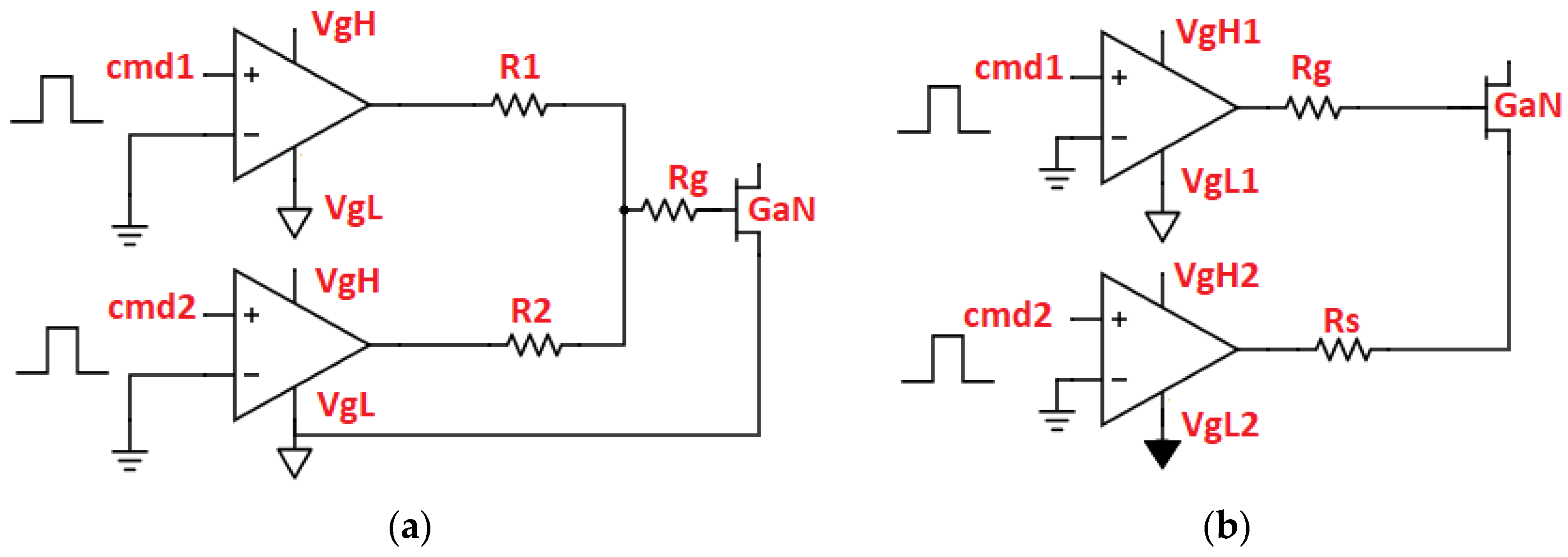
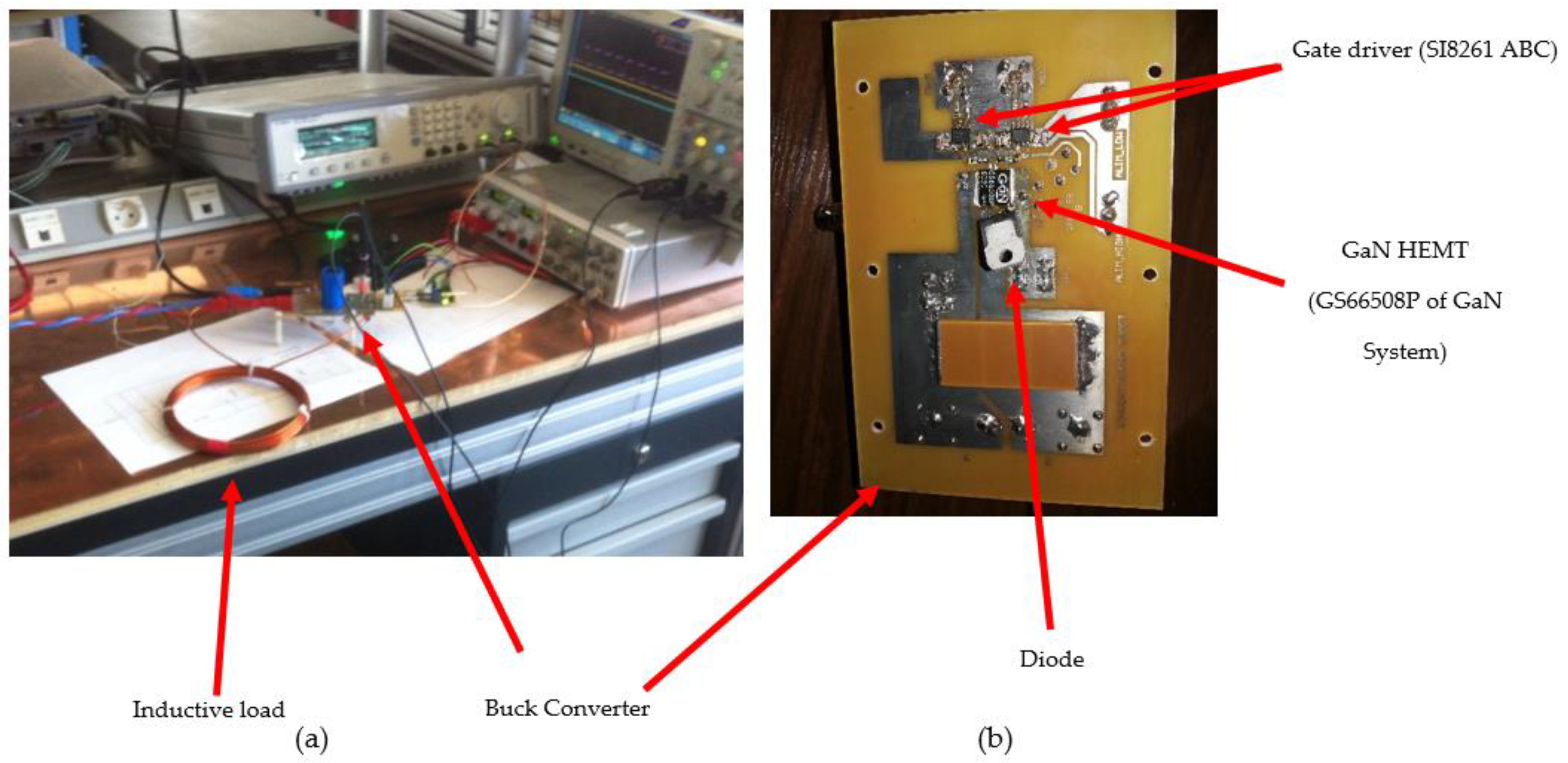
3. Experimental Setup and Results for AGVC Open-Loop Control

To evaluate the interests of the active gate-voltage control, the circuit in Figure 1 was used as the test prototype (the gate driver circuit configuration-2 in Figure 3 was built using two SI8261ABC drivers from Silicon Labs) [23]. The diver has a minimum supply voltage of 6.5 V (high-to-low > 6.5 V), which limits the application to the GS66508P as it can easily exceed the absolute gate voltage limit of 7 V in the continuous mode [24]. Since the converter was tested in a pulsed mode, the GaN HEMT can be well controlled under 10 V (pulsed limit voltage) without any damage. For the continuous mode of operation, the SI8261ABC driver is not recommended. The experimental setup and the converter prototype are shown in Figure 4. Figure 5, Figure 6, Figure 7, Figure 8, Figure 9 and Figure 10 illustrate the experimental results of AGVC-based design and a comparison of the SGVC results obtained during turn-on.

4. Experimental Results with an Open-Loop Active Gate Voltage Control
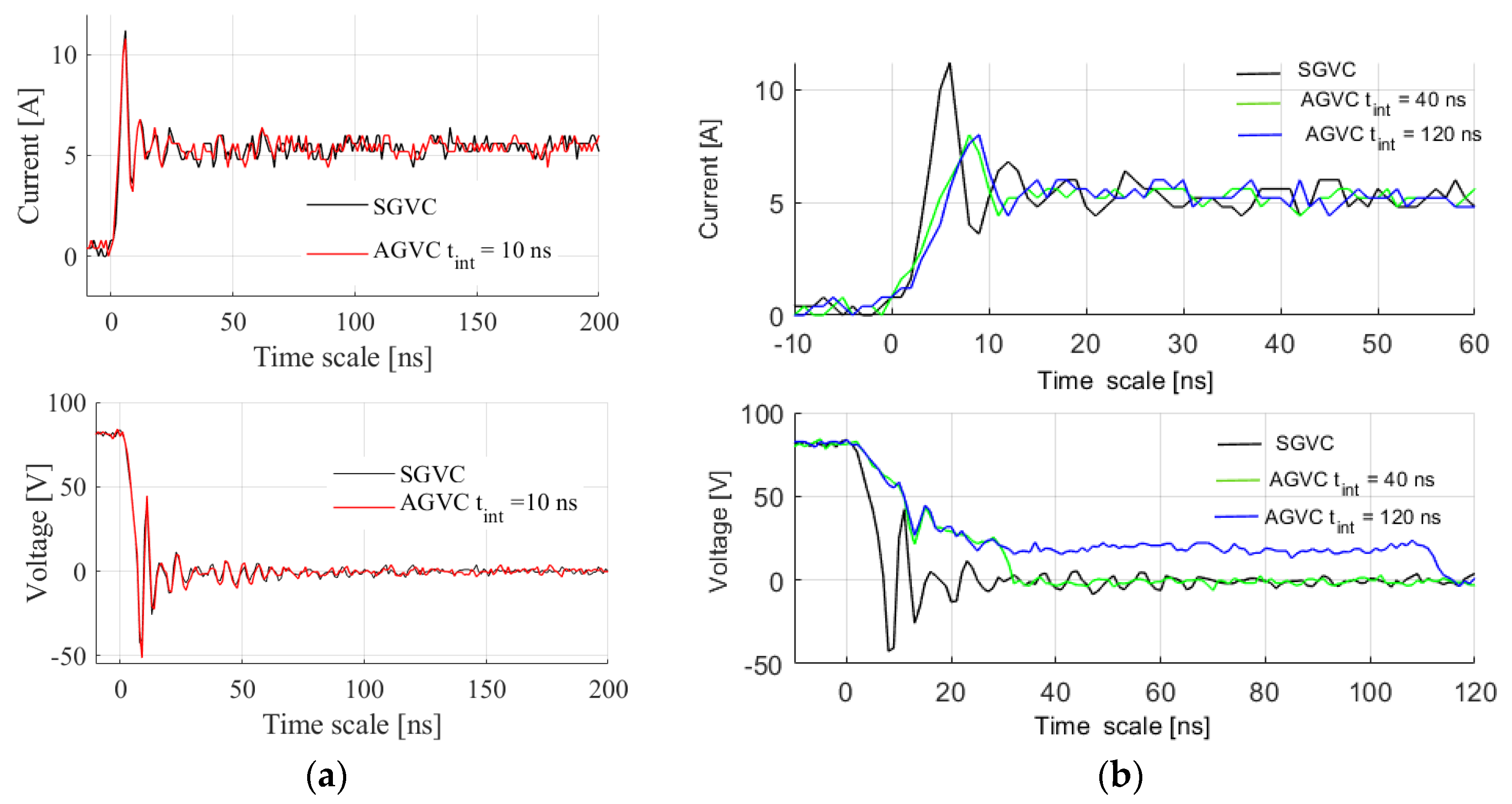
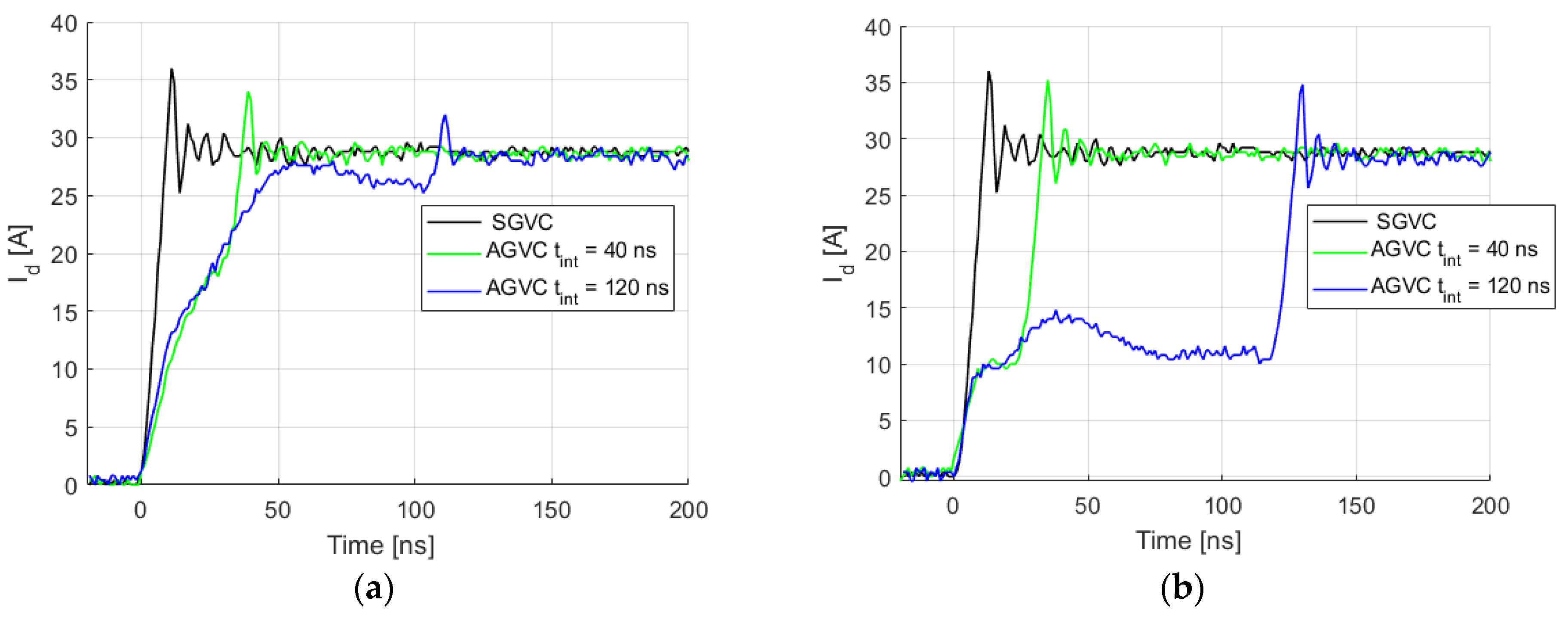
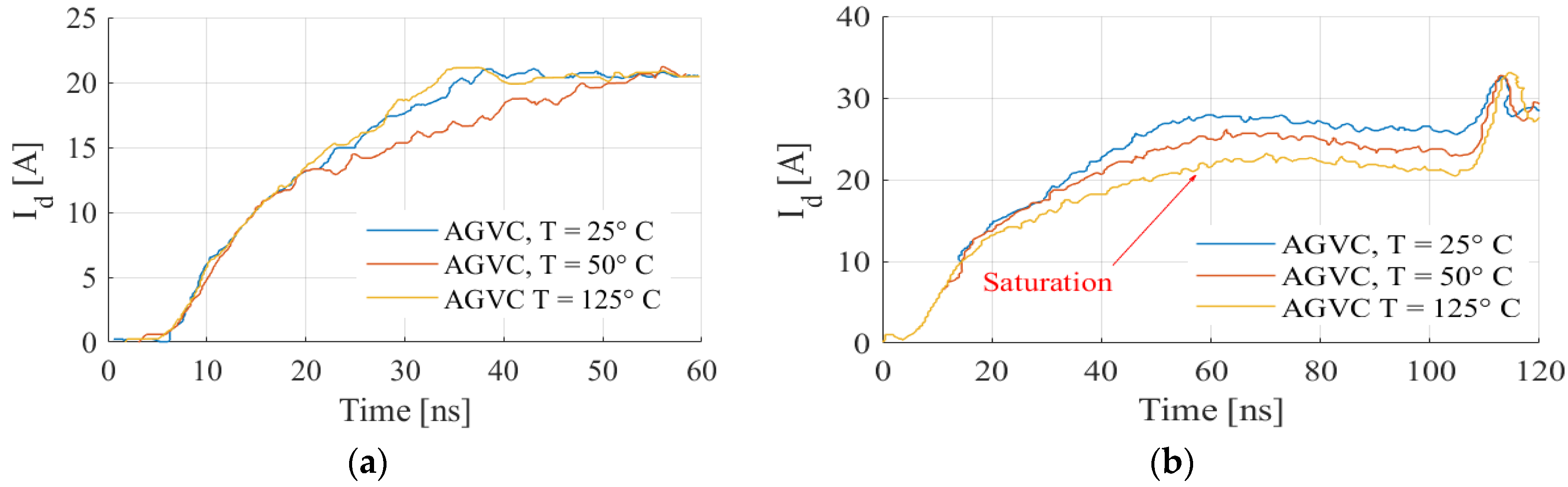
4.1. Parameter tint

To assess the impact of tint in the AGVC voltage pattern, two cases were tested using the GS66508P GaN transistor with Vth = 1.2 V. In the first case, an intermediate voltage of 4 V (Vgrint = 4 V) was applied for a very short duration of tint (tint ≤ 10 ns). For the second case, the voltage Vgrint is applied for a longer time (tint > 10 ns). Figure 6 compares the results of the two cases.
As seen in the results, the signals obtained with the SGVC and the AGVC for a duration of tint of 10 ns are identical, which implies the AGVC gate voltage cannot slow down di/dt for a short duration of tint (tint < 10 ns) of a GaN transistor (Figure 6a). The long response time of the driver (SI8261ABC) can be the main cause of the impossibility of being able to slow the di/dt of the GaN transistor when applying the AGVC technique.
With an increase in the duration of tint, the AGVC slow down the di/dt because the drain current takes more time than the SGVC to reach the load current (Figure 6b). For low load currents (ILoad = 5 A), the same di/dt is obtained with a tint of 40 ns and a tint of 120 ns (Id of Figure 6b). However, they do not have the same impact on the switching speed of the voltage. The larger the tint (120 ns), the greater the effect on the dv/dt (Vds in Figure 6b). To reduce conduction losses, it is essential to minimize the tint dependent effect on the dv/dt when applying AGVC.
Due to the operation of the GaN transistor in the linear zone (during the turn-on switching phase), the application of a long tint (120 ns) can also have other negative consequences. As illustrated as a red arrow of Figure 7b and Figure 8, an appearance of the saturation phenomenon occurred in high load currents. Because, during the application of the intermediate voltage (Vgrint), the transistor has reached its maximum current for the given Vgrint. In order to avoid the generation of additional losses due to the saturation phenomenon, the value of tint must be optimized. A closed-loop AGVC can be applied to optimize the value of tint, which corresponds to the moment when the drain current id reached its final value (load current). Furthermore, the saturation current increases with the increase in Vgrint (Figure 7a) whereas it decreases with increasing temperature (Figure 8). The GaN characteristics deteriorate with the increase in temperature. As can be seen in Figure 8, the increase in temperature also causes a decrease in di/dt obtained with the AGVC action (Figure 8a). To limit these negative effects, a closed-loop control requires adjusting tint and Vgrint dynamically for each operating point.

4.2. Switching Losses during Turn-On

A comparison of the energy losses and variations in di/dt among the applications of AGVC and SGVC are summarized in Table 1. The di/dt varies from 2.5 A/ns to 0.5 A/ns with the application of AGVC (with 4 V of Vgrint during 40 ns of tint). When the tint value increases to 120 ns, similar di/dt can be obtained, but the losses are increasing. To approach a similar di/dt (0.8 A/ns) using the SGVC (Rg is 39 Ω), the losses are even more prominent than those obtained using the AGVC with Vgrint being 4 V and tint being 40 ns.
As seen in Table 2, the extra losses introduced in AGVC are less important than those related to the SGVC (Rg = 39 Ω) when the saturation phenomenon occurs. However, the AGVC is less advantageous in the case of large tint due to the high impact on dv/dt.

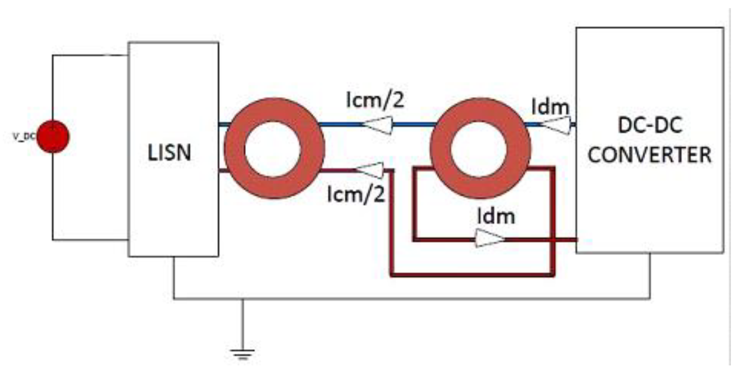
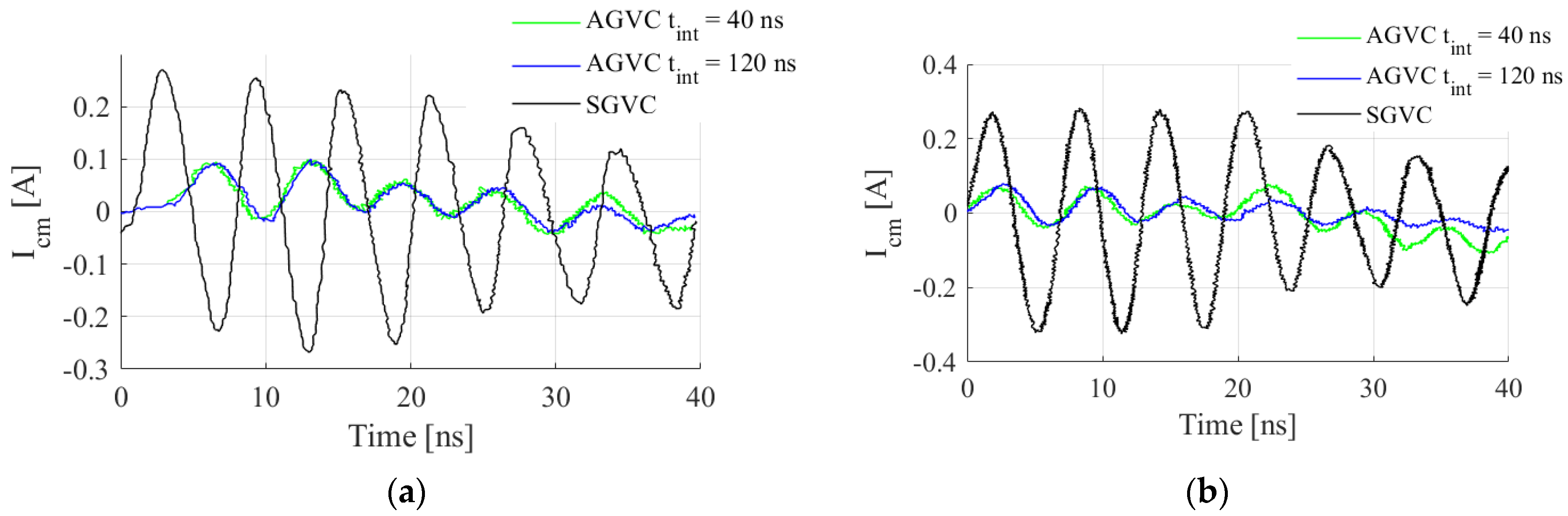
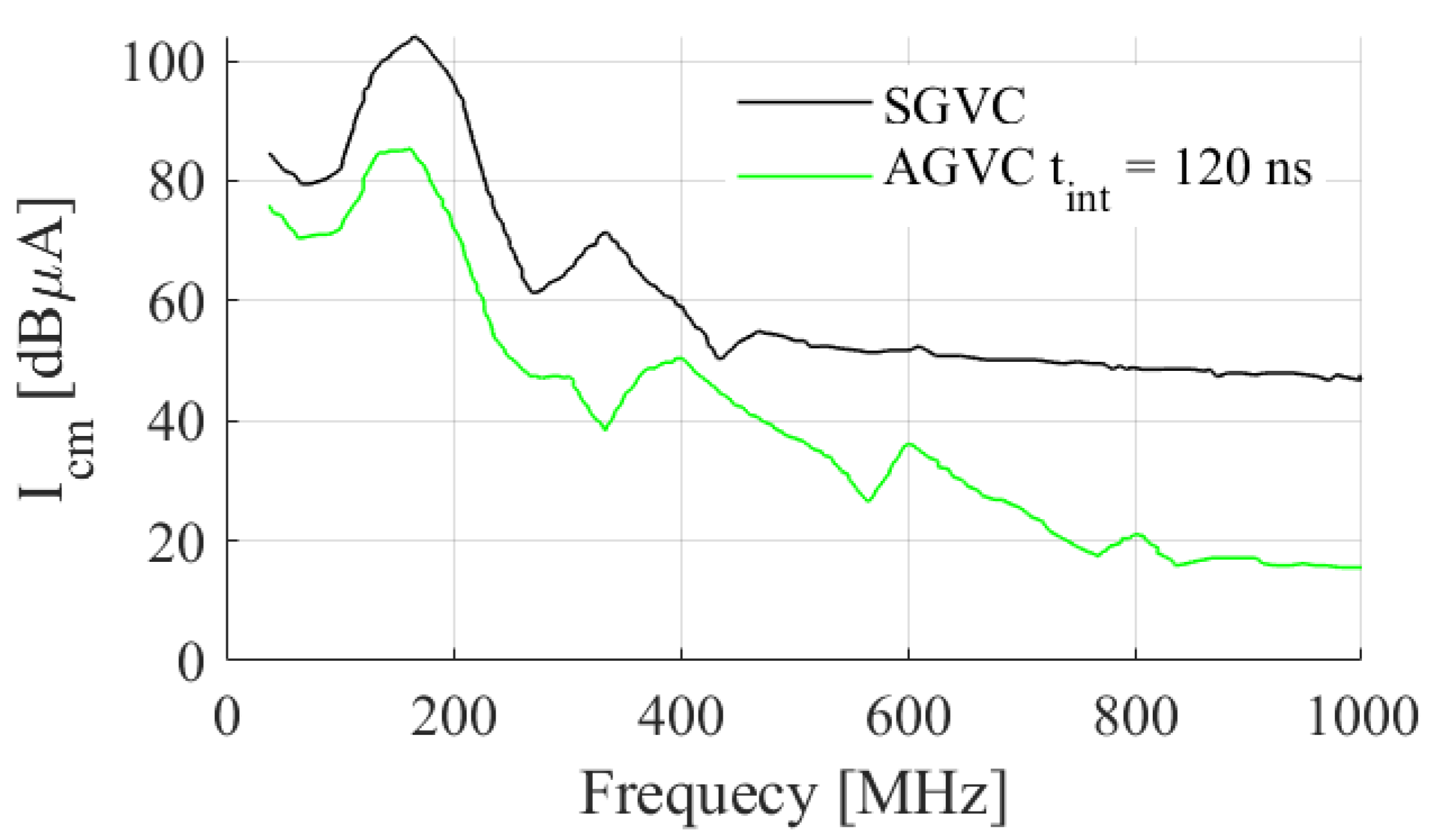
4.3. Impact of AGCV on Conducted Electromagnetic Disturbances

The results obtained in the previous parts imply that it is possible to slow down the GaN switching speeds at turn-on with AGVC. GaN high switching speed and high-frequency operation generate oscillations in common mode current waveforms that AGVC may help attenuate. Oscillations introduce conducted disturbances that are studied in time and frequency domains using the test bench illustrated in Figure 9. In these experiments, the common mode current (Icm) and the differential mode current are measured using magnetic probes (Pearson current monitor model 6595). Figure 10 and Figure 11 show the experimental results.
The reduction of the di/dt obtained with AGVC allows attenuating the common mode currents compared to that of the SGVC (Figure 10). The variation of the di/dt caused by the variation of the drain current (current from 2 A to 6 A), causes an increase in Icm from 20 ns for a tint of 40 ns and a current of 6 A (Figure 10b) compared for the same tint but for a current of 2 A (Figure 10a). These analyses confirm the conclusions concerning the need to set up a closed-loop control in order to keep the di/dt constant, allowing to have a constant Icm current. Regarding the oscillation frequency, the AGVC has no impact. This is the reason why the two peaks observed in the frequency domain with the two controls (AGVC and SGVC) occur at the same frequency (175 MHz and 600 MHz). A reduction of 20 dBµA is obtained with the AGVC for a tint of 120 ns.

5. Closed-Loop Active Gate Voltage Control

In the AGVC, di/dt and dv/dt vary with the operating point of the transistor and the power converter parameters. To overcome these issues, a closed-loop AGVC can be applied.

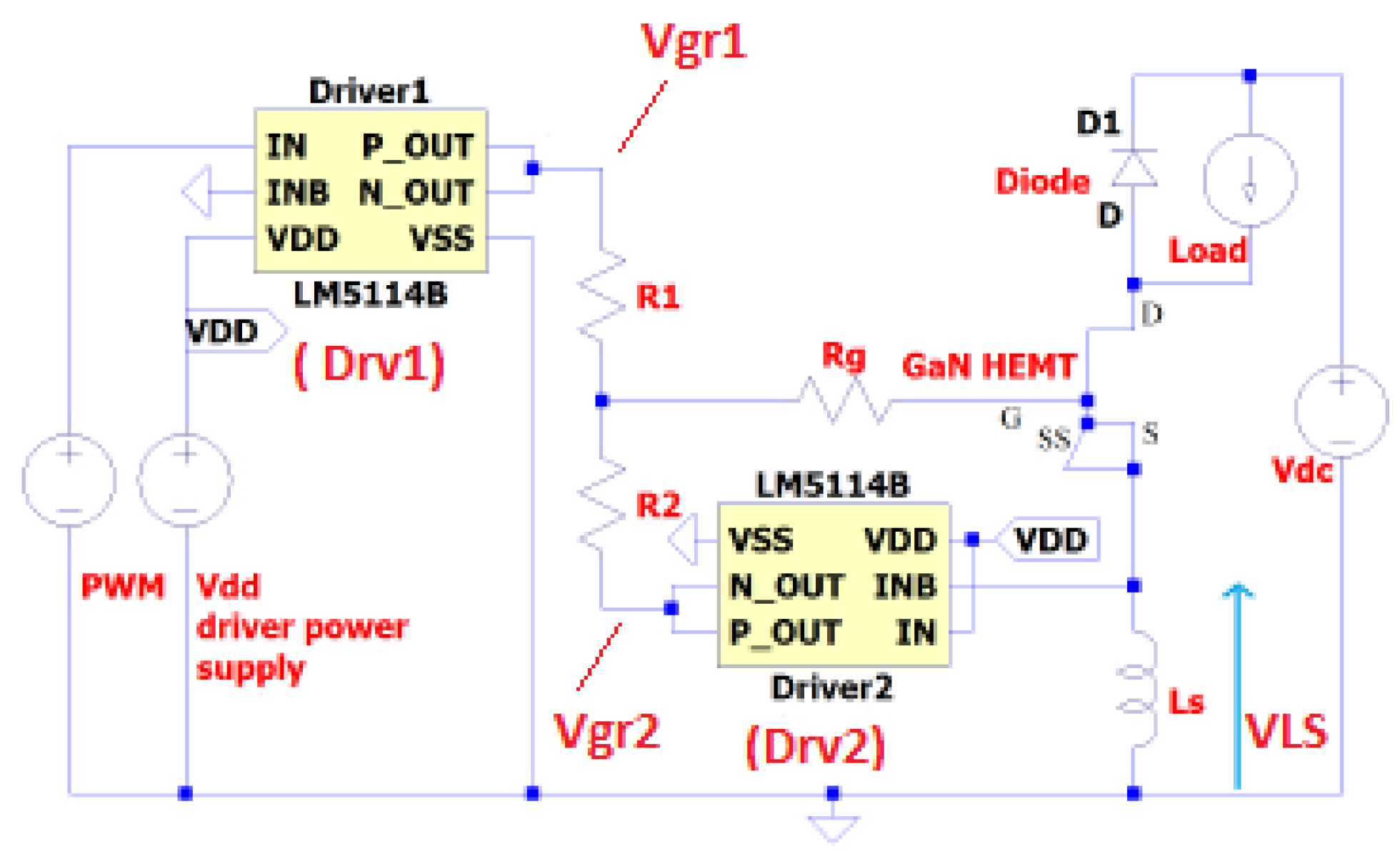
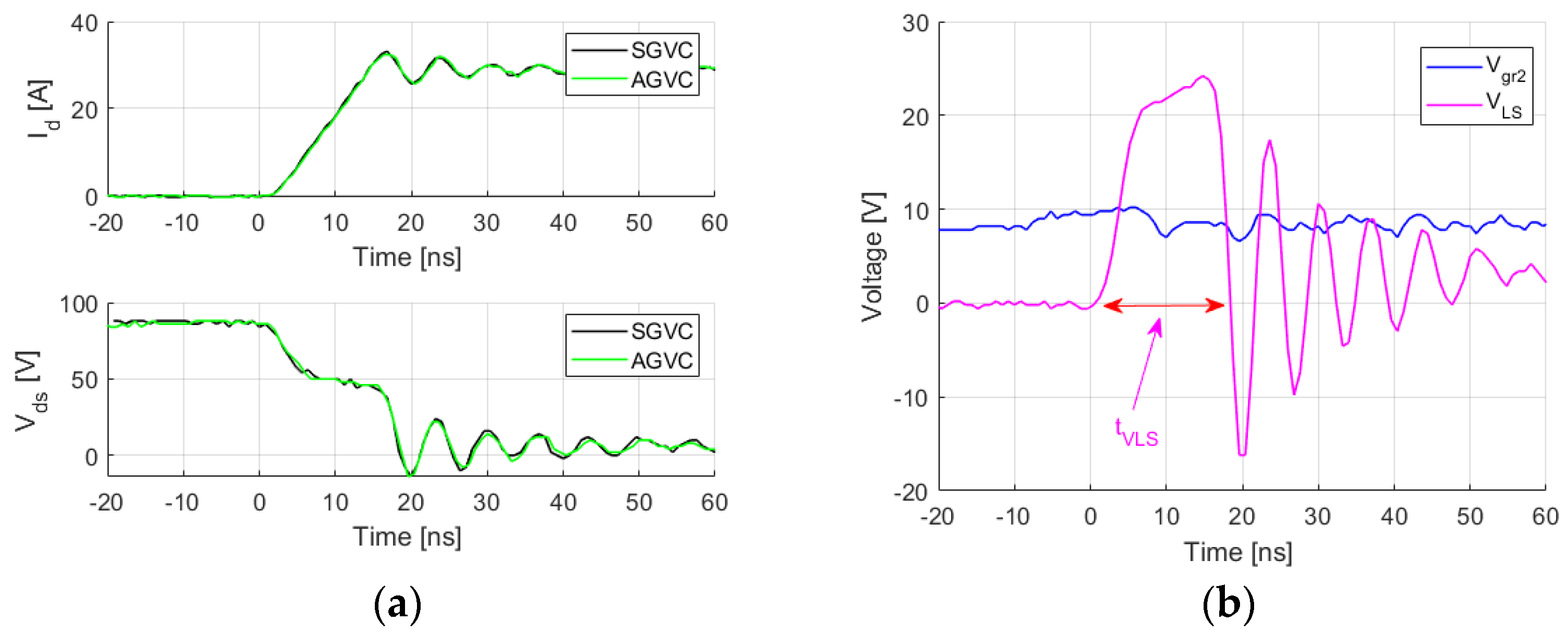
5.1. Closed-Loop AGVC with Common Source Parasitic Inductance during Turn-On

The closed-loop control uses the configuration-1 of the AGVC structure in Figure 3. The voltage VLs created by the drain current during turn-on is used to control the driver 2 (Drv2) (Figure 12). At the beginning of the turn-on (t = [0 t1]), the drain current Id is zero as Vgs is less than Vth, and the voltage at the terminal of Ls (VLs) is zero. Since the signal related to Ls is connected to the inverse input of driver-2. The control voltage of the GaN transistor is the output voltage of the driver-1 (the output of the driver-2 being in the high-impedance state for VLs is 0).
The output voltage of the driver-1 (Vgr1) will increase until reaching the threshold voltage of the GaN (Vth) at t1, which causes a positive variation of the drain current and, thereby, the positive variation of VLs (VLs > 0 V) (Figure 13). Depending on the peak value (VLsmax and its duration (tVLs), four cases are possible, but only one has an effect on di/dt.
When the maximum value (VLsmax of VLs is larger than the minimum input voltage of the driver-2 (2.5 V) with a sufficient duration of the tVLs, the output of the driver-2 (Vgr2) reaches the low state that will allow controlling the GaN device with an intermediate gate voltage (Vgrint). This will slow down the switching speed of the current (Figure 13a). The other three cases are where the peak value (either or both VLsmax of parasitic inductance and its duration tVLs) is insufficient to create a low state at the output of the driver-2. In these three cases, there will be no reduction of Id (Figure 13b). It is a type of “binary” AGVC as, according to the load current, the di/dt is controlled (as in the first case) or not (other cases).

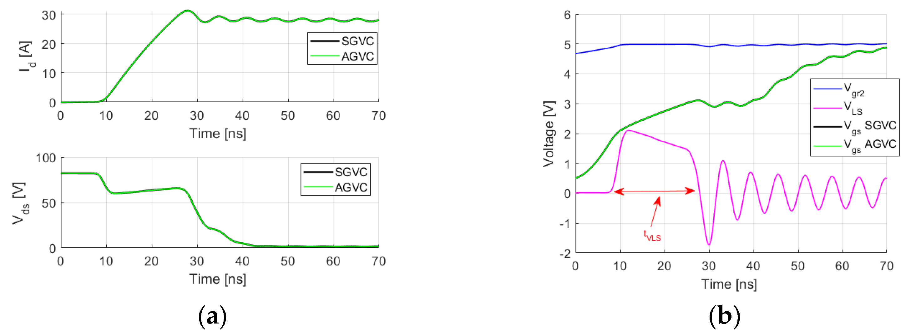
5.1.1. Simulation Results

The circuit in Figure 12 is simulated for a parasitic inductance of 1 nH (Ls = 1 nH) and a drain current of 28 A (Figure 12). The proposed closed-loop control circuit does not slow down the switching speed of the current because the VLsmax obtained during the di/dt is lower than the minimum activation voltage of the LM5114 driver (Figure 14). However, by increasing the value of Ls to 2 nH for the same drain current (Id = 28 A), a sufficient input voltage is applied to the input of driver-2 (Figure 15b) that enables the LM5114 (driver-2) that allows us to slow down di/dt (Figure 15b). The significant delay time (20 ns Figure 15b) of LM5114 drivers compared to the switching time of the GaN transistor makes this closed-loop control have more effect on the dv/dt than the di/dt (Figure 15b).

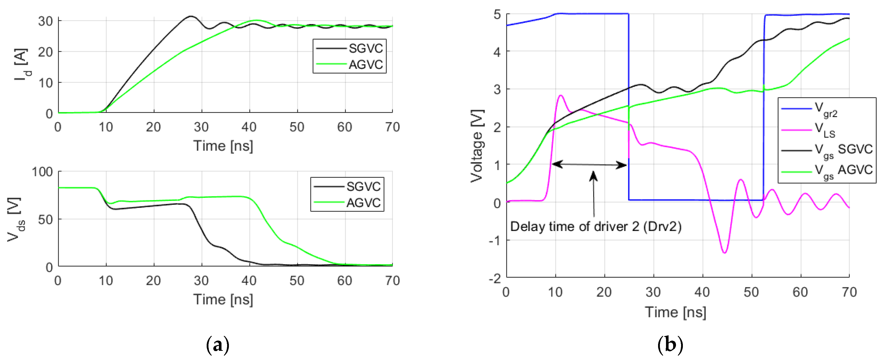
5.1.2. Experimental Results

A circuit with 2 nH of Ls as illustrated in Figure 12 was experimentally analyzed and the results are presented in Figure 16. For a load current between 5 and 20 A, the experimental circuit cannot slow down the current switching speed like the predictions of the simulation evaluation. The voltage across Ls (VLmax) is larger than the minimum activation voltage of the LM5114 driver (2.5 V). A fair assumption has been made on the driver operation, which the inactivation of the driver is due to a small application time, tVLs, of VLmax. Therefore, the application of such a circuit requires a driver capable of reacting to an input signal shorter than or equal to 15 ns.

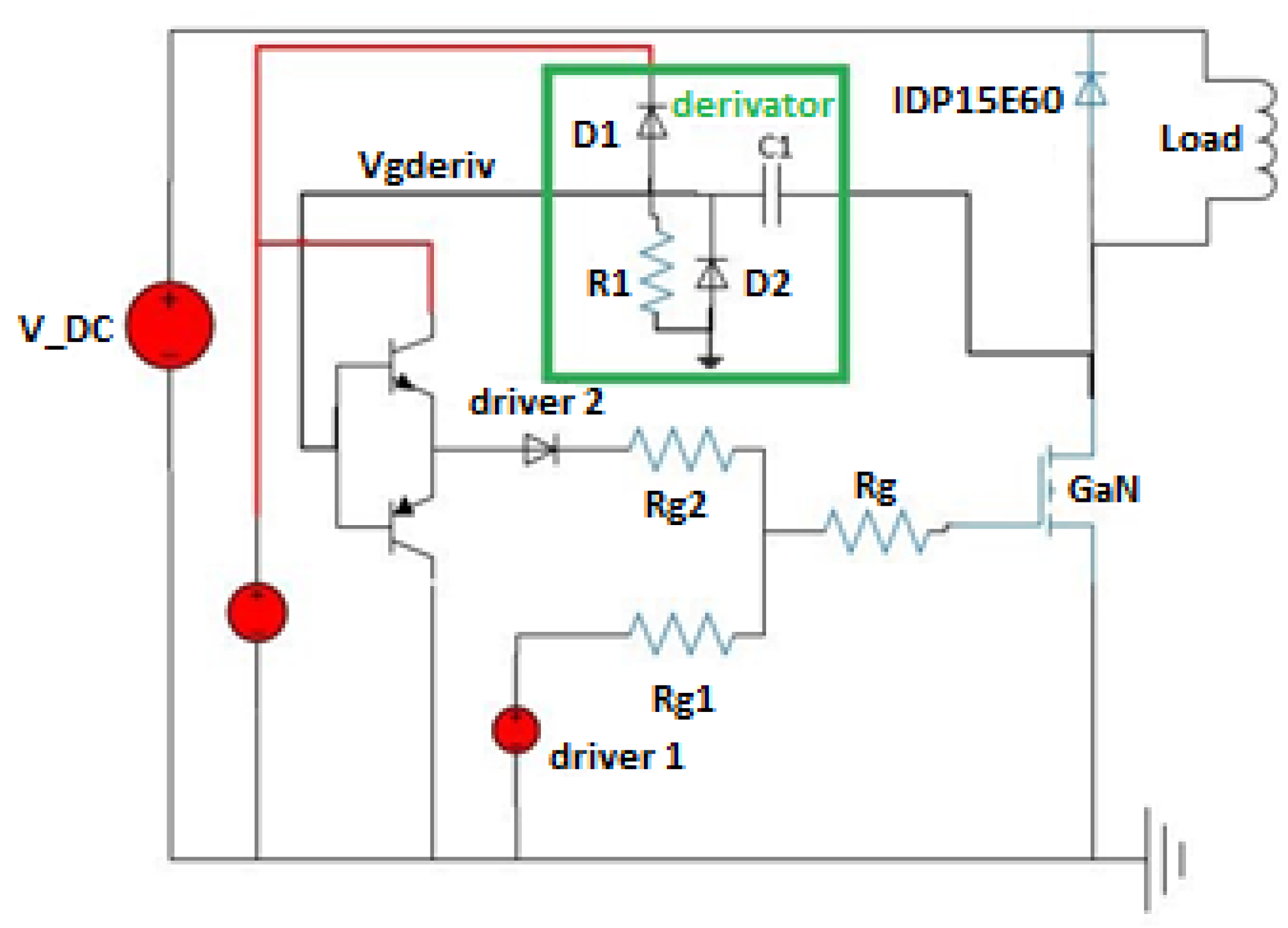
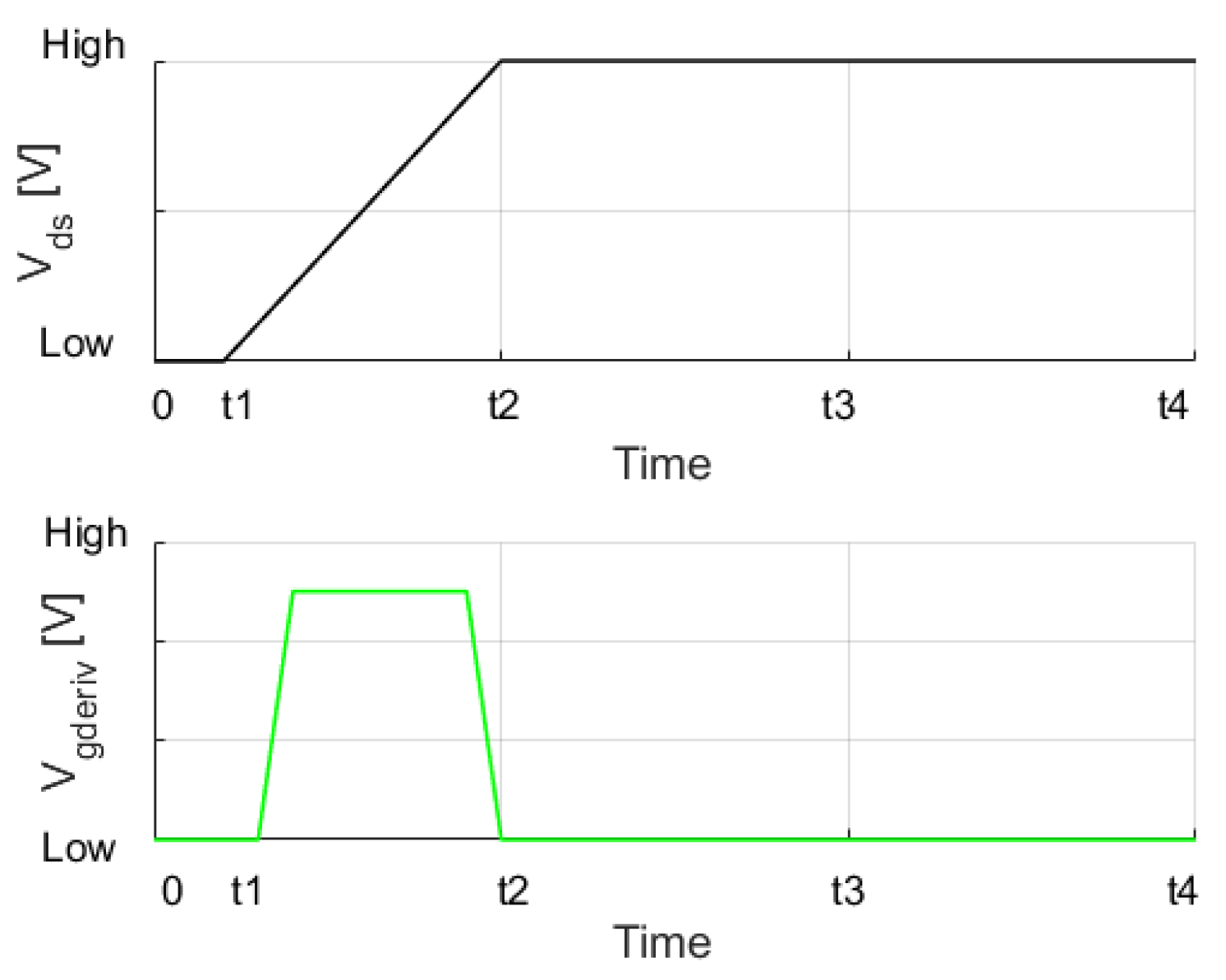
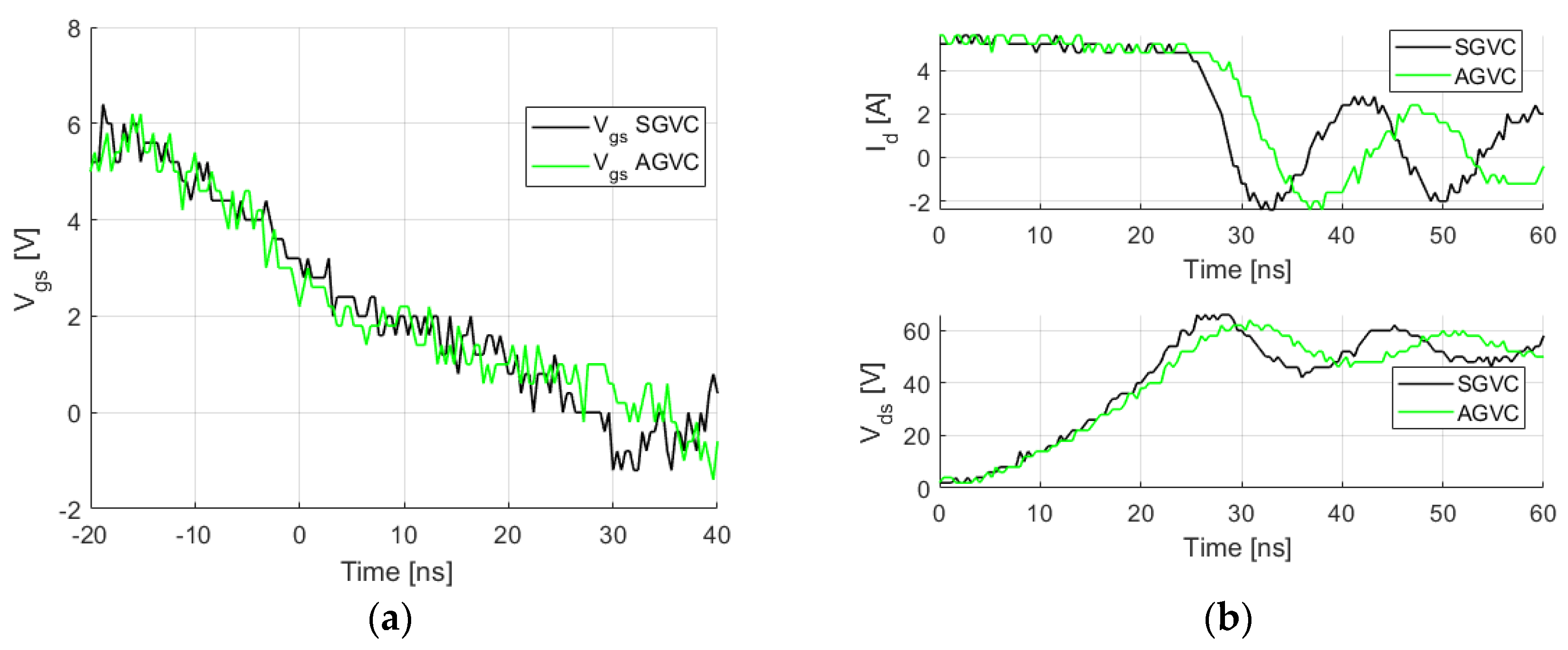
5.2. Closed-Loop AGVC with a Derivative Circuit during Turn-Off

In this approach, the drain voltage Vds can be used to tune the parameter tint of the circuit (Figure 17 and Figure 18), which comprise a resistor (R1), two diodes (D1, D2), and a capacitor (C1). At the beginning of the turn-off phase of the GaN transistor, a zero voltage can be applied to the cathode terminal of D2 and to the anode terminal of D1 while keeping the control signal Vgderiv low. The increase in the drain voltage (Vds) ensures the forward biasing of diodes D1 and D2 and produces a high-level control signal Vgderiv. At the end of the turn-off transient, the control signal Vgderiv turns back to a low level (Figure 18 and Figure 19).
An experimental prototype of the circuit in Figure 17 was implemented. At the initial turn-off of the GaN transistor (see graphs during time 0 to 10 ns in Figure 20), the Vgs signals are identical for both gate voltage controls (i.e., standard gate voltage control and AGVC closed-loop control for the turn-off). The drain voltage (Vds) is lower than the voltage supply of the derivative circuit of the driver (Vgrmax) during initial turn-off. Hence, the Vgderiv signal is in a low state. After 15 ns, the voltage Vds is higher than the voltage Vgrmax. Therefore, the Vgderiv signal increases (Figure 21). The proposed circuit applies an intermediate gate-source voltage starting from 15 ns. The ratio of the voltage transient speed of AGVC to SGVC is 0.97 as seen in Table 3.
As seen in the results, the speed of the current transients has not reduced significantly. Therefore, the losses are not in the case of the open-loop control. The switching waveform of the drain current depends on several parameters. The first parameter is the response time of the driver that causes a significant delay in the output voltage of the driver (Vgr). The di/dt is reduced with an increase in Vgr. The closed-loop control system is more efficient when the supply voltage is above 100 V for a similar load current (i.e., 10 A as seen in Table 3). This technique has less impact on the current at high voltages when the switching time is large enough to compensate the response times of the driver. The second parameters are the resonance of the capacitance, resistance, and parasitic inductance of the circuit. To address this issue, a flip-flop is necessary to capture only one high-state event in the control signal Vgderiv.

6. Conclusions

Initially, the feasibility of controlling di/dt and dv/dt across GaN transistors in the open-loop gate control was studied with an experimental analysis. Despite its high switching speed, an application of the open-loop AGVC technique can be used to reduce the switching speed by 90% compared to a passive technique, resulting in a 50% reduction in the switching losses. Although the open-loop AGVC can be used to obtain fewer switching losses compared to the standard gate voltage control, it has many issues, such as the inability to control switching transient time of the power device less than 10 ns, and the difficulty of imposing similar transition patterns when the operating point vary. Furthermore, the variation of the experimental conditions (i.e., temperature, voltage, and current) affects the reduction rate in transient time. In order to solve these problems, a less complex AGVC-based closed-loop strategy was proposed. It was possible to manage the switching transients on the variation of the experimental conditions. However, due to the long response times (>10 ns) of the Si-based discrete components in the control circuit, it only solved these problems partially. However, by implementing a GaN-based monolithic circuit, the delays in the control loop can be eliminated.

Author Contributions

M.L.B. is the main investigator of this research. T.W. and J.F.M. have mainly contributed to the implementation of experimental measurements. L.V.P. has participated in research work with numerical simulations. N.I. has contributed toward implementing the active regulation loop (AGVC). H.M. (proof) and B.A. (proof) have supervised the research. All authors have read and agreed to the published version of the manuscript.

Funding

This research received no external funding.

Institutional Review Board Statement

Not applicable.

Informed Consent Statement

Not applicable.

Data Availability Statement

No data available.

Conflicts of Interest

The authors declare no conflict of interest.

References

  1. Colin, D.; Rouger, N. High speed optical gate driver for wide band gap power transistors. In Proceedings of the 2016 IEEE Energy Conversion Congress and Exposition (ECCE), Milwaukee, WI, USA, 18–22 September 2016; pp. 1–6. [Google Scholar]
  2. Bindra, A. Wide-Bandgap Power Devices: Adoption Gathers Momen-tum. IEEE Power Electron. Mag. 2018, 5, 22–27. [Google Scholar] [CrossRef]
  3. Rodrguez, M.; Zhang, Y.; Maksimovic, D. High-frequency PWM buck converters using GaN-on-SiC HEMTs. IEEE Trans. Power Electron. 2014, 29, 24622473. [Google Scholar] [CrossRef]
  4. Wu, Y.-F.; Gritters, J.; Shen, L.; Smith, R.P.; Swenson, B. kV-class GaN-on-Si HEMTs enabling 99% efficiency converter at 800 V and100 kHz. IEEE Trans. Power Electron. 2014, 29, 26342637. [Google Scholar] [CrossRef]
  5. Moench, S.; Costa, M.; Barner, A.; Kallfass, I.; Reiner, R.; Weiss, B.; Waltereit, P.; Quay, R.; Ambacher, O. Monolithic integrated quasi-normally-off gate driver and 600 v gan-on-sihemt. In Proceedings of the 2015 IEEE 3rd Workshop on Wide Bandgap Power Devices and Applications (WiPDA), Blacksburg, VA, USA, 2–4 November 2015; pp. 92–97. [Google Scholar]
  6. Zhang, Z.; Wang, F.; Tolbert, L.; Blalock, B. Active gate driver for crosstalk suppression of SiC devices in a phase-leg configuration. IEEE Trans. Power Electron. 2014, 29, 1986–1997. [Google Scholar] [CrossRef]
  7. Wang, J.; Liu, D.; Dymond, H.C.P.; Dalton, J.J.O.; Stark, B.H. Crosstalk suppression in a 650-V GaN FET bridge-leg converter using 6.7-GHz active gate driver. In Proceedings of the Energy Conversion Congress and Exposition (ECCE) 2017 IEEE, Cincinnati, OH, USA, 1–5 October 2017; pp. 1955–1960. [Google Scholar]
  8. Li, H.; Li, X.; Zhang, Z.; Yao, C.; Wang, J. Design consideration of high power GaN inverter. In Proceedings of the 2016 IEEE 4th Workshop on Wide Bandgap Power Devices and Applications (WiPDA), Fayetteville, AR, USA, 7–9 November 2016; pp. 23–29. [Google Scholar]
  9. Rossigno, T. A Contribution to the Characterization and Gate Driver Control of Wide Band GAP for Medium Voltage of Inverter. Ph.D. Thesis, Institut National Polytechnique de Toulouse, Toulouse, France, 28 May 2015. [Google Scholar]
  10. Chen, Y.; Lee, F.C.; Amoroso, L.; Wu, H. A resonant MOSFET gate driver with efficient energy recovery. IEEE Trans. Power Electron. 2004, 19, 470–477. [Google Scholar] [CrossRef]
  11. Galluzzo, A.; Melito, M.; Belverde, G.; Musumeci, S.; Raciti, A.; Testa, A. Switching characteristic improvement of modern gate controlled devices. In Proceedings of the 1993 Fifth European Conference on Power Electronics and Applications, Brighton, UK, 13–16 September 1993; pp. 374–379. [Google Scholar]
  12. Takizawa, S.; Igarashi, S.; Kuroki, K. A new di/dt control gate drive circuit for IGBTs to reduce EMI noise and switching losses. In Proceedings of the PESC 98 Record. 29th Annual IEEE Power Electronics Specialists Conference, Fukuoka, Japan, 22–22 May 1998; Volume 2, p. 1443144. [Google Scholar]
  13. Chen, L. Intelligent Gate Drive for High Power MOSFETs and IGBTs. Ph.D. Thesis, Department of Electrical and Computer Engineering, Michigan State University, East Lansing, MI, USA, 2008. [Google Scholar]
  14. Hemmer, R. Intelligent IGBT drivers with exceptional driving and protection features. In Proceedings of the 13th European Conference Power Electronics and Application, Barcelona, Spain, 8–10 September 2009. [Google Scholar]
  15. Wang, Z.; Shi, X.; Tolbert, L.M.; Wang, F.; Blalock, B.J. A di/dt feedback-based active gate driver for smart switching and fast overcurrent protection of IGBT modules. IEEE Trans. Power Electron. 2014, 29, 37203732. [Google Scholar] [CrossRef]
  16. Idir, N.; Bausiere, R.; Franchaud, J. Active gate voltage control of turn-on di/dt and turn-off dv/dt in insulated gate transistors. IEEE Trans. Power Electron. 2006, 21, 849–855. [Google Scholar] [CrossRef]
  17. Grbovic, P. An IGBT gate driver for feed-forward control of turn-on losses and reverse recovery current. IEEE Trans. Power Electron. 2008, 23, 643–652. [Google Scholar] [CrossRef]
  18. Park, S.; Jahns, T.M. Flexible dv/dt and di/dt control method for insulated gate power switches. IEEE Trans. Ind. Appl. 2003, 39, 657–664. [Google Scholar] [CrossRef]
  19. John, V.; Suh, B.; Lipo, T.A. High-performance active gate drive for high-power IGBT’s. IEEE Trans. Ind. Appl. 1999, 35, 1108–1117. [Google Scholar] [CrossRef] [Green Version]
  20. Sun, B.; Burgos, R.; Zhang, X.; Boroyevich, D. Active dv/dt Control of 600V GaN Transistors. In Proceedings of the IEEE Energy Conversion Congress and Exposition (ECCE), Milwaukee, WI, USA, 18–22 September 2016; p. 18. [Google Scholar]
  21. Bau, P.; Cousineau, M.; Cougo, B.; Richardeau, F.; Colin, D.; Rouger, N. A CMOS gate driver with ultra-fast dv/dt embedded control dedicated to optimum EMI and turn-on losses management for GaN power transistors. In Proceedings of the 14th Conference on Ph.D. Research in Microelectronics and Electronics (PRIME), Prague, Czech Republic, 2–5 July 2018. [Google Scholar]
  22. Beye, M.L.; Mogniotte, J.F.; Phung, L.V.; Idir, N.; Maher, H.; Allard, B. Analysis and Assessment of temperature effect on an Open Loop Active Gate Voltage Control of GaN Transistor during Turn-ON and Turn-OFF. In Proceedings of the 13th IEEE International Conference on Power Electronics and Drive Systems (PEDS), Toulouse, France, 9–12 July 2019. [Google Scholar]
  23. SI8261 ABC Datasheet. Available online: https://www.silabs.com/documents/public/data-sheets/Si826x.pdf (accessed on 1 June 2018).
  24. GS66508P Datasheet. Available online: https://gansystems.com/wp-content/uploads/2018/02/GS66508P-DS-Rev-180213.pdf (accessed on 1 June 2018).
Figure 1. A simplified schematic of a transistor/diode switching cell in a buck configuration.
Electronics 10 00106 g001
Figure 2. Typical gate driver signals: (a) standard two stage gate-drive control signal, (b) di/dt turn-on control using AGVC.
Electronics 10 00106 g002
Figure 3. Possible gate drive circuit configurations for AGVC: (a) configuration-1 with a common-voltage at the source, (b) configuration-2 with a varying voltage at the source.
Electronics 10 00106 g003
Figure 4. (a) Test setup and (b) the prototype.
Electronics 10 00106 g004
Figure 5. Vgs waveforms (Rg = 3 Ω and Vgrint = 4 V).
Electronics 10 00106 g005
Figure 6. Vds and Id waveforms depending on parameter tint of AGVC (current load 5 A, Rg = 3 Ω and Vgrint = 4 V): (a) low tint (tint = 10 ns), (b) high tint (tint > 10 ns).
Electronics 10 00106 g006
Figure 7. Current waveforms during turn-on using AGVC for different load current values and different tint values. (a) Vgrint = 4 V, (b) Vgrint = 3.5 V.
Electronics 10 00106 g007
Figure 8. Drain current waveforms during turn-on for different temperature values (Rg= 3 Ω and Vgrint = 4 V, tint = 120 ns) (a) Id = 20 A, (b) Id = 28 A.
Electronics 10 00106 g008
Figure 9. Test bench for conducted emission measurements with current probes.
Electronics 10 00106 g009
Figure 10. Common mode current (Icm) during turn-on for Rg = 3 Ω, Vgrint = 4 V, and Vdc = 50 V, (a) Id = 2 A, (b) Id = 6 A.
Electronics 10 00106 g010
Figure 11. Common mode current (Icm) during turn-on in a frequency domain for load current of 6 A, Rg = 3 Ω, Vgrint = 4 V, and Vdc = 50 V.
Electronics 10 00106 g011
Figure 12. Schematic diagram of the proposed closed-loop AGVC using a common source parasitic inductance (Ls).
Electronics 10 00106 g012
Figure 13. Simulated signals of the proposed circuit: (a) case 1, (b) case 2.
Electronics 10 00106 g013
Figure 14. Simulated waveform of the main voltage and current using the proposed closed-loop active gate voltage circuit (AGVC) and standard gate voltage control (SGVC) (Id = 28 A, Ls = 1 nH), (a) Vds and Id, (b) VLs, Vgr2, Vgs of AGVC, and Vgs of SGVC.
Electronics 10 00106 g014
Figure 15. Simulated waveform of the main voltage and current using the proposed closed-loop active gate voltage circuit (AGVC) and standard gate voltage control (Id = 28 A, Ls = 2 nH), (a) Vds and Id, (b) VLs, Vgr2, Vgs of AGVC and Vgs of SGVC.
Electronics 10 00106 g015
Figure 16. Experimental waveform of the main voltage and current using the proposed closed-loop active gate voltage circuit (AGVC) and standard gate voltage control (SGVC) (Id = 28 A, Ls = 2 nH), (a) Vds and Id, (b) VLs, Vgr2, Vgs of AGVC and Vgs of SGVC.
Electronics 10 00106 g016
Figure 17. Schematic diagram of the proposed AGVC closed-loop during turn-off.
Electronics 10 00106 g017
Figure 18. Schematic diagram of a derivative circuit.
Electronics 10 00106 g018
Figure 19. Simulated control signal of the driver (Vgderiv) during GaN transistor turn-off.
Electronics 10 00106 g019
Figure 20. Experimental waveforms of the AGVC closed-loop voltage control compared to the standard gate voltage control (Id = 5 A, V_DC = 50 V), (a) Vgs, (b) Vds and Id.
Electronics 10 00106 g020
Figure 21. Input signal of Vgr2.
Electronics 10 00106 g021
Table 1. Comparison of energy losses using AGCV and standard gate control with load current without saturation (Id = 5 A).
di/dt [A/ns]dv/dt [V/ns]Eon [µJ]
AGVC (Rg = 3 Ω and tint = 40 ns)0.8−2.66.6
AGVC (Rg = 3 Ω and tint = 120 ns)0.8−0.7414
Standard gate voltage control (Rg = 3 Ω)1.5−1.82.6
Standard gate voltage control (Rg = 39 Ω)0.6−1.813
Table 2. Comparison of energy losses using AGCV and standard gate control with load current without saturation (Id = 28 A).
di/dt [A/ns]dv/dt [V/ns]Eon [µJ]
AGVC (Rg = 3 Ω and tint = 40 ns)0.84−339
AGVC (Rg = 3 Ω and tint = 120 ns)0.48−0.9189
Standard gate voltage control (Rg = 3 Ω)3.2−10.812
Standard gate voltage control (Rg = 39 Ω)1.2−0.750
Table 3. Performances of closed loop of AGVC and standard gate control circuits during the turn-off.
AGCV di/dt [A/ns]SGCV di/dt [A/ns]AGCV dv/dt [V/ns]SGCV dv/dt [V/ns]di/dt
(AGVC/SGVC)
dv/dt
(AGVC/SGVC)
V_DC = 100 V
Id = 5 A
0.610.664.450.920.88
V_DC = 100 V
Id = 10 A
1.311.565.345.60.80.95
V_DC = 50 V
Id = 10 A
1.561.63.53.620.980.97
Publisher’s Note: MDPI stays neutral with regard to jurisdictional claims in published maps and institutional affiliations.

