The Alignment Method for Linear Scale Projection Lithography Based on CCD Image Analysis †
by
 ,
,
Dongxu Ren
1,* ,
,
Jianpu Xi
1,
Zhengfeng Li
1,
Bin Li
1,
Zexiang Zhao
1,
Huiying Zhao
2,
Lujun Cui
1 and
Hang Xu
1 1
Zhongyuan University of Technology, Zhengzhou 450007, China
2
State Key Laboratory for Manufacturing Systems Engineering, Xi’an Jiaotong University, Xi’an 710049, China
*
Author to whom correspondence should be addressed.
†
Presented at the 4th International Electronic Conference on Sensors and Applications, 15–30 November 2017; Available online: http://sciforum.net/conference/ecsa-4.
Proceedings 2018, 2(3), 101; https://doi.org/10.3390/ecsa-4-04936
Published: 15 November 2017
(This article belongs to the Proceedings of The 4th International Electronic Conference on Sensors and Applications)
Abstract
:This paper presents a method to improve the alignment accuracy of mask in linear scale projection lithography, in which the adjacent pixel gray square variance method of CCD image is used to find the best position of the focal length of the motherboard and then realize the alignment of the focal plane. Two image positions in the focal plane from the CCD are compared the traits overlap through the image splicing principle, and to establish the correction of four typical errors on the basis of the whole grating errors. At the same time, using the rotation error of the mask to summarize Grayscale Variation Function of CCD Image, and threshold functions are used to express the factors including wave crests of the amplitude, period error and phase error, which govern the rotation accuracy and weight alignment accuracy expression of the four error factors is established. In the experiment, it is finally corrected the slope of the mask and be adjusted the same direction of the slide plate with the help of dual-frequency laser interferometer, the influence of alignment error on lithography accuracy was discussed and verified in the static case and the CCD maximum resolution pixel corresponds to 0.1 μm, the accuracy of scale is 0.79 μm in only 200 mm measurement range.
1. Introduction
Grating lithography alignment is one of the main influencing factors to improve the accuracy of projection lithography. Through precise focal plane alignment of the projection lithography system, the pattern of the mask is projected accurately on the surface of the scale plane with the positive or negative photoresist, and reduce the impact of the alignment error on the accuracy of grating lithography process in a certain motion range. The alignment of the grating lithography is characterized by uniform grating stripes and a certain length, so it is a major technical problem that when the lithography plate or mask behave a tilting or rotating phenomenon, this installation error will seriously affect the accuracy of the linear scale.
Several lithography methods are used for alignment, such as in proximity lithography, a modified coarse-fine alignment scheme was designed for proximity lithography based on four-quadrant-grating moiré [1,2], moiré fringe precision alignment is being used in nanoimprint lithography [3], and the digital moiré fringe measurement method for alignment be studied in imprint lithography [4], finding optimal higher-order alignment adjustment under the purpose of maximizing die yields in semiconductor lithography equipment [5], in which all the lithography, any alignment methods can not suit for the projection lithography. Alignment marks are selected by discussing the relevant criteria in projection electron lithography [6], and new alignment mark design structures are used for higher diffraction order wafer quality enhancement [7]. All these lithography methods are not required for long-range precision alignment.
However, linear scale lithography emphasizes the uniformity between the same lines with 20 μm pitch. Some else study, an ultraprecision stages are designed to align wafers for the microlithography of integrated circuit [8], which includes the rich variety of lines, and the different patterns or traits are being lithography on wafers based on various alignment techniques, and these method such as thermally controlled alignment [9] and the wafer rear surface and canceling tilt effect [10] do not concerned about the consistency of the lines.
In the long-distance lithography process of the linear scale studied in this paper, alignment error, motion displacement, length of grating, installation tilt angle of grating, the straightness error of mobile workbench and the installation precision repeatability affect directly or indirectly the alignment accuracy of linear scale projection lithography, which affects the lithography accuracy of the linear scale and methods are less studied using CCD based on interferometry. Through the simulation and experiment of this paper, we give the analysis and verification about the influence of the mask tilt and rotation error on the accuracy of the lithography alignment, and the analysis of the image resolution based on the CCD image are carried out, ultimately to achieve a high precision alignment.
2. Method
2.1. Principle for Accuracy Alignment
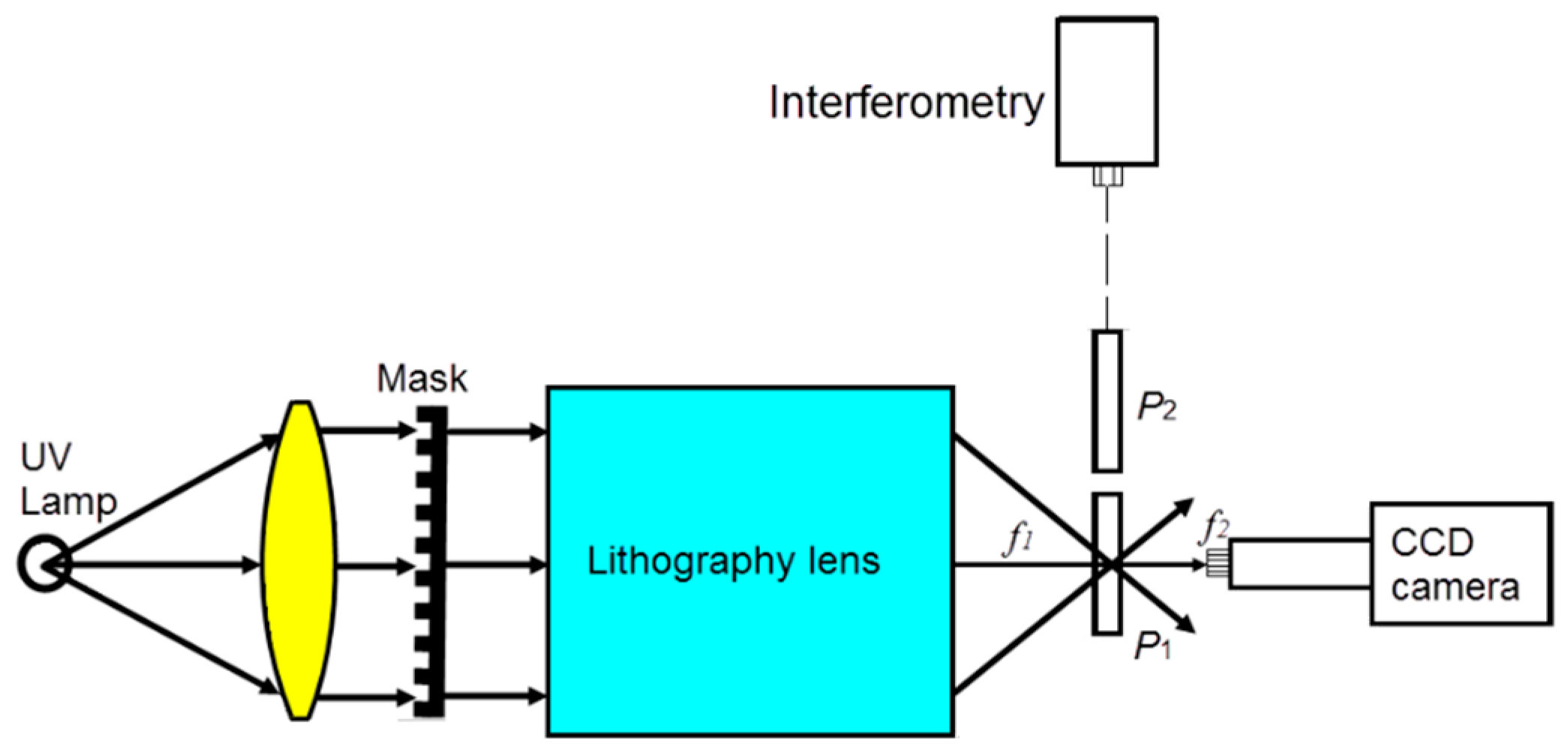
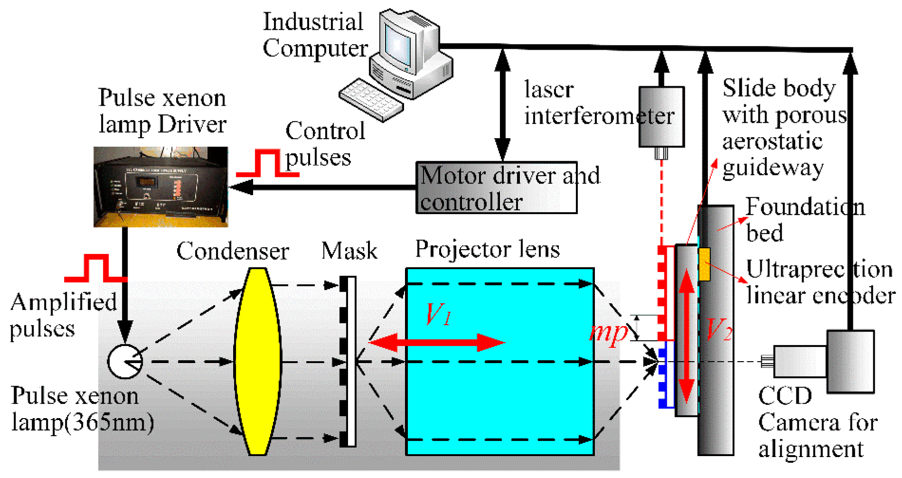
The fundamental principles of projection lithography alignment for high precision linear scale is illustrated in Figure 1. First, adjust the focal length of the CCD sensor so that it is aligned with the grating focal plane. Second, mount the custom mask plate into the projection lithography lens system, adjust the spatial position of the lithography lens, then ensure that the focal length is aligned with the grating focal plane by monitoring the clarity of the CCD image, in which the tilt adjustment method and the sharpness algorithm are two important points of alignment. The next step, adjust the installation mask tilt based on the direction of movement of the table, and then comply with abbe principle to align the dual-frequency laser interferometer movement direction and workbench movement in the same direction, which can make sure the base surface of grating and dual-frequency laser interferometer optical path in a straight line, while adjusting the rotation mounting error based on a specific algorithm.
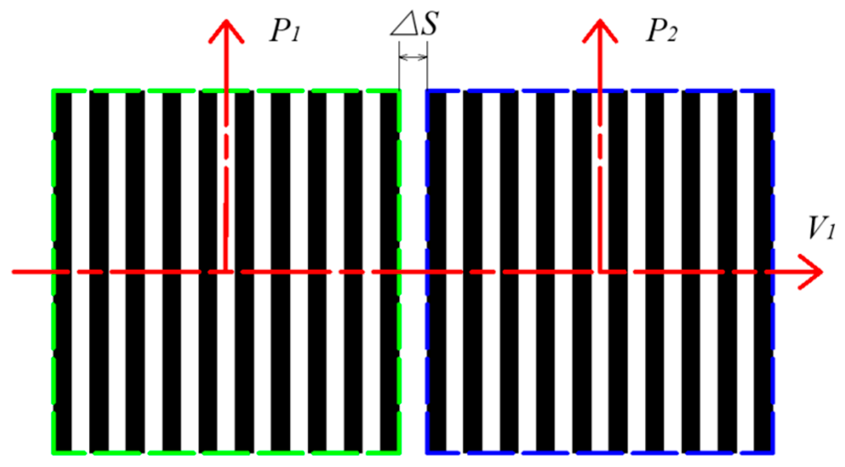
According to some constant distance, a grating graphic window step by another accurately projection lithography to form a linear scale. To complete the high precision grating scale in the lithography manufacturing, the tilt grating on the mask mounted in lithography lens which is one critical part of the alignment accuracy must be check out, as shown in Figure 2, the following formula 1 position relationship:
and which represent gratings vertical direction, both parallel to each other, and be formed by the two complete separate lithography steps, the step I and the step II. represents the slide body, Which movement direction of the experimental setup.
2.2. Tilt Mask Alignment
In grating projection lithography process, two key factors profound impact on mask plate alignment, includes the precision focus and tilt mask alignment, which’s alignment accuracy and the accuracy of grating is proportional. Figure 3 shows the several grating imagines caused by the different tilt angles in the grating projection lithography process, docking error accumulated by the whole linear scale can be expressed as
where L represents the total length of the grating lithography, m represents the times of lithography at the whole length L, represents i-th lithography error caused by temperature fluctuations, represents i-th lithography error caused by vibration disturbance, represents uncertainty of measurement feedback.
2.3. Rotation Mask Alignment
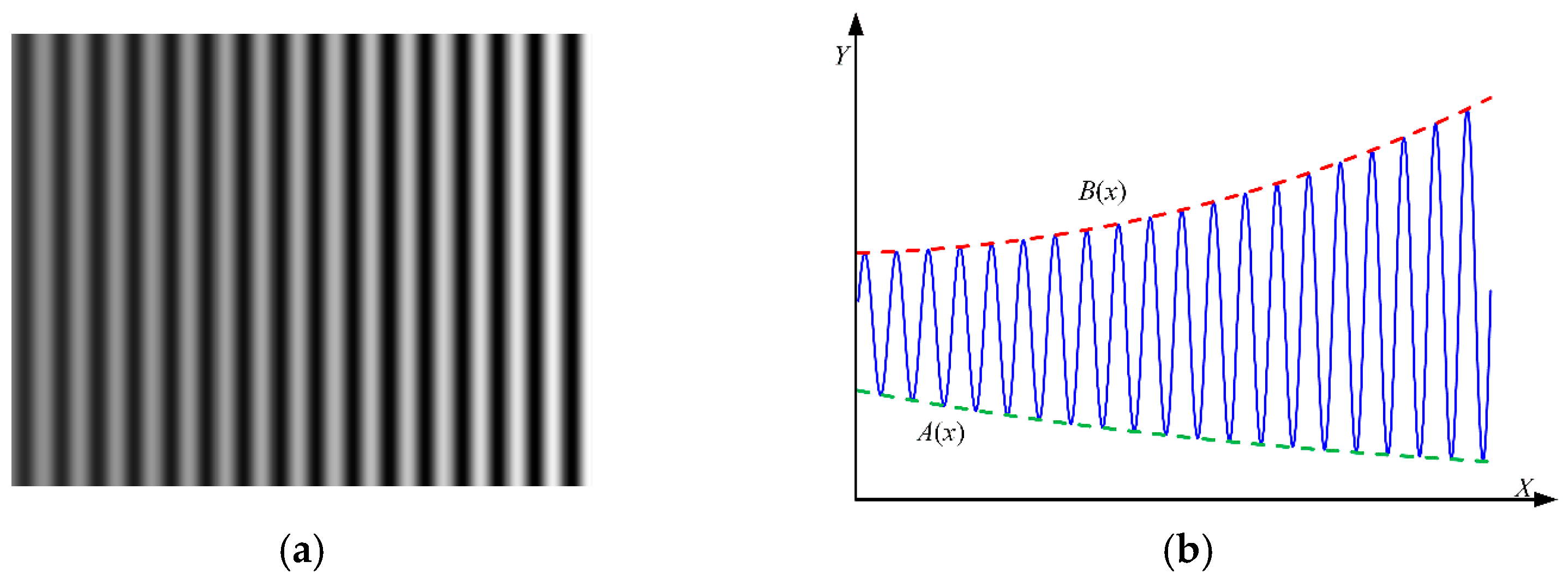
The rectangular wave with period is evenly changed, the change interval is (0, 255) and the amplitude is , where the rising and falling edges reflect the sharpness, and which is expressed by the amount of changed angle in the time domain space domain, the ideal angle is , and which is expressed as high frequency components in the frequency domain.
Figure 4 shows tilting legend of mask, which can get curve trend including A(x,y) and B(x,y). Thus, the complex characterization formula can be simplified, in the lithography alignment process, the alignment error of the amplitude, phase and period on the functions and will be achieved the convergence of different alignment accuracy, then complete different alignment accuracy adjustment, the boundary expression is as follows:
where can be described as .
, and are amplitude wave errors, amplitude trough errors, pitch periodic errors, and phase errors. These parameters affect the alignment accuracy according to different weights, which can be expressed as:
3. Alignment Experiments
3.1. Align the Focal Plane Based on CCD Image
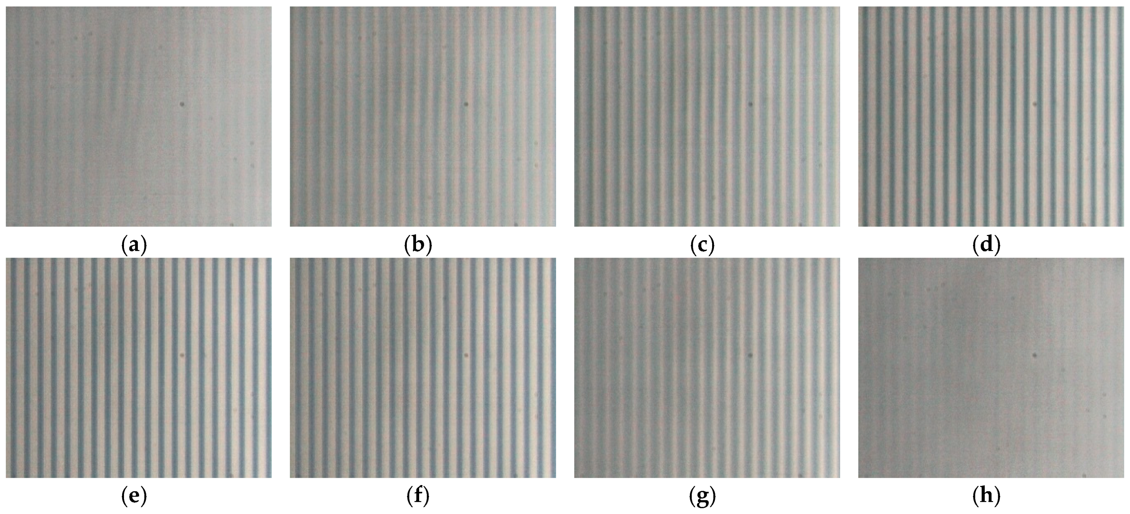
The purpose of the alignment experiment is to verify the accuracy of CCD image alignment principle, to ensure when the lithography is ready, the grating mask is precisely projected onto the photoresist plane, and to form a higher resolution CCD image in the focal plane. As shown in Figure 5 a–f, the image acquisition of different focus positions is measured by micro-CCD sensor. It can be seen that the image is blurred to clear, and then there is a clear to fuzzy change process oppositely. The gray value of the cross section is extracted by the gray value change curve extracted in Figure 5a–f, and then the adjacent pixel gray variance method is used and normalized [11]. The maximum value is the most clear picture, and the focal length of the corresponding, with its evaluation function to get the value and the normalized value shown in Table 1.
From the above experimental results, it can be seen that the criterion of image evaluation has strong single peak, and the most clear image can be distinguished, and the alignment effect of photolithography plane is realized, and the accuracy of grating lithography is improved objectively.
3.2. Align Tilt Mask with Laser Interferometer
In the experiment, the commonly linear scale projection lithography splice process is replaced by the average homogenization technique that overlap the different position pitch regularly [12]. we use splicing lithography method for alignment, and lithography process including coating, before drying, lithography, development, post-baking, hardening, corrosion. Positive photoresist using BP series, and the resolution of up to 0.1 μm.
As shown in Figure 6, the is the first photolithographic position, moving through the control system and the laser feedback system in the direction by 4.800 mm, reaching the position and performing the photolithography, and applying the photolithography process to develop. Three corrections are performed on the basis of the photolithography test to obtain the result shown in Figure 7. By performing the focusing process in the above flow chart, the BC value is reduced to reach the error range and the alignment method is verified.
3.3. Influence of Alignment Error on Lithography Accuracy
Figure 8 shows the lithography precision alignment error discussed in this section is mainly in the static case, that is, before the lithography process through a full length of the static calibration of multiple points to achieve the focal length alignment, while in the grating lithography process, the main factors that affect the focal length alignment error includes movement straightness of the guideway direction, clamping error of the blank grating, vibration of the moving process, which caused overlap deviation between the focal plane and the photoresist plane of the blank grating.
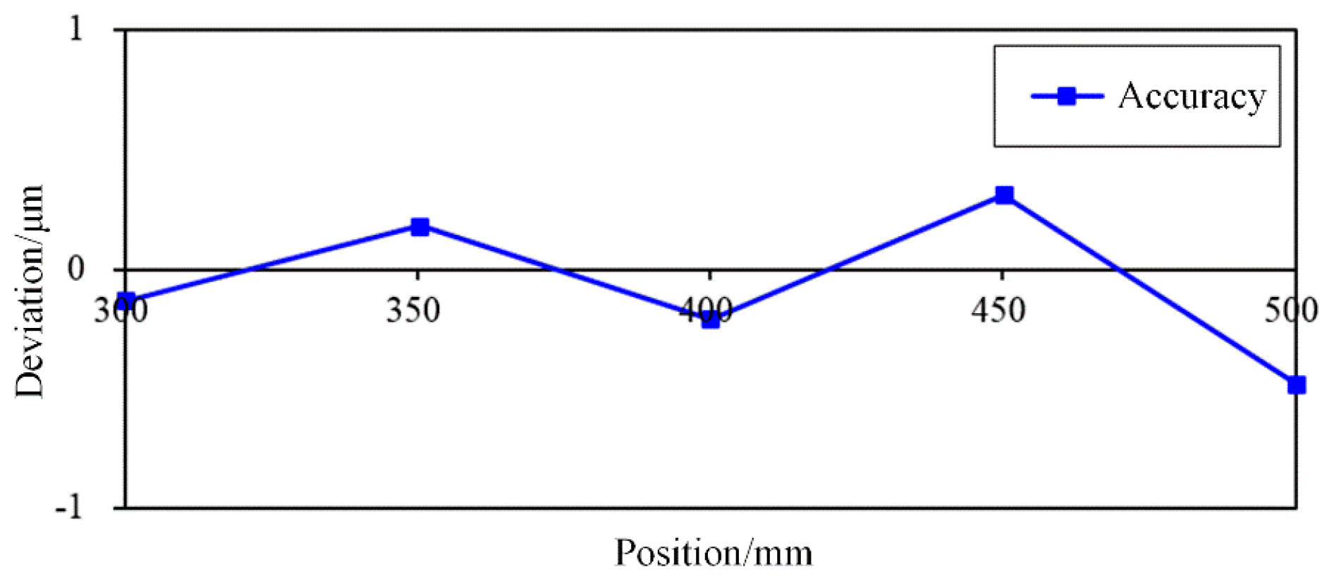
Then, through experimental verification, when the tilt angle is aligned as shown in Section 3.2, considering the uncertain factors and the laser displacement sensor pitch alignment, the CCD maximum resolution pixel corresponds to 0.1 μm, while reducing the influence of other parameter factors. As shown in Figure 9, the accuracy of scale is 0.79 μm in only 200 mm measurement range.
4. Conclusions
(1) The optimal position of the focal plane of the mask is determined by the CCD image; (2) In the plane alignment, four kinds of conventional tilt cases are listed, and the mathematical model is used to interpret the method, the plane tilt tolerance error is described with view of the theoretical point; (3) the Fourier algorithm of the lithography lens system is used to model the tilt errors, the alignment accuracy function of the rotation error is characterized by the weighting of the errors.
Experimental results show the lithography alignment method was verified, and the lithography process was carried out based on CCD and mathematical algorithm, then lithography accuracy of scale is 0.79 μm in only 200 mm measurement range.
Acknowledgments
This project is supported by National Natural Science Foundation of China (Grant No. 51475485, 51705546, 51505506) and Beijing International Science and Technology Cooperation (BaseUltra-precision processing and measurement equipment development and production).
Conflicts of Interest
The authors declare no conflict of interest.
References
- Di, C.; Zhu, J.; Yan, W.; Hu, S. A modified alignment method based on four-quadrant-grating moiré for proximity lithography. Opt. Lasers Eng. 2014, 125, 4868–4872. [Google Scholar] [CrossRef]
- Zhu, J.; Hu, S.; Zhou, P.; Yu, J. Experimental study of Talbot imaging moiré-based lithography alignment method. Opt. Lasers Eng. 2014, 58, 54–59. [Google Scholar] [CrossRef]
- Li, N.; Wu, W.; Chou, S.Y. Sub-20-nm Alignment in nanoimprint lithography using moiré fringe. Nano Lett. 2006, 6, 2626–2629. [Google Scholar] [CrossRef] [PubMed]
- Shao, J.; Ding, Y.; Tian, H.; Li, X.; Li, X.m.; Liu, H. Digital moiré fringe measurement method for alignment in imprint lithography. Opt. Laser Technol. 2012, 44, 446–451. [Google Scholar] [CrossRef]
- Miyashiro, R.; Fukagawa, Y. Optimization of alignment in semiconductor lithography equipment. Precis. Eng. 2009, 33, 327–332. [Google Scholar] [CrossRef]
- Farrow, R.C.; Liddle, J.A.; Berger, S.D.; Huggins, H.A.; Kraus, J.S.; Camarda, R.M.; Tarascon, R.G.; Jurgensen, C.W.; Kola, R.R.; Fetter, L. Marks for alignment and registration in projection electron lithography. J. Vac. Sci. Technol. B Nanotechnol. Microelectron. 1993, 11, 240–246. [Google Scholar] [CrossRef]
- Zhang, L.; Feng, Y.; Dong, L.; Su, X.; Tian, Z.; Fang, C.; Wei, Y.; Ye, T. New alignment mark design structures for higher diffraction order wafer quality enhancement. SPIE Adv. Lithogr. 2017, 10145, 101452C. [Google Scholar] [CrossRef]
- Lee, C.W.; Kim, S.W. An ultraprecision stage for alignment of wafers in advanced microlithography. Precis. Eng. 1997, 21, 113–122. [Google Scholar] [CrossRef]
- Sreenivasan, S.V. Thermally controlled alignment for wafer-scale lithography. J. Micro/Nanolithogr. MEMS MOEMS 2013, 12, 031109. [Google Scholar] [CrossRef]
- Terasawa, T. Novel alignment technique for 0.1-μm lithography using the wafer rear surface and canceling tilt effect. Opt. Eng. 1993, 32, 2344–2349. [Google Scholar]
- Qian, Q.; Zang, D.D. A modified sharpness-evaluation function of image based on sobel. Comput. Digit. Eng. 2015, 10, 1865–1870. [Google Scholar]
- Ren, D.; Zhao, H.; Zhang, C.; Yuan, D.; Xi, J.; Zhu, X.; Ban, X.; Dong, L.; Gu, Y.; Jiang, C. Multi-repeated projection lithography for high precision linear scale based on average homogenization effect. Sensors 2016, 16, 538. [Google Scholar] [CrossRef] [PubMed]
Figure 1.
Scheme of system for accuracy alignment on the projection lithography.

Figure 2.
The ideal splicing scheme for two CCD images in the process of precision alignment.

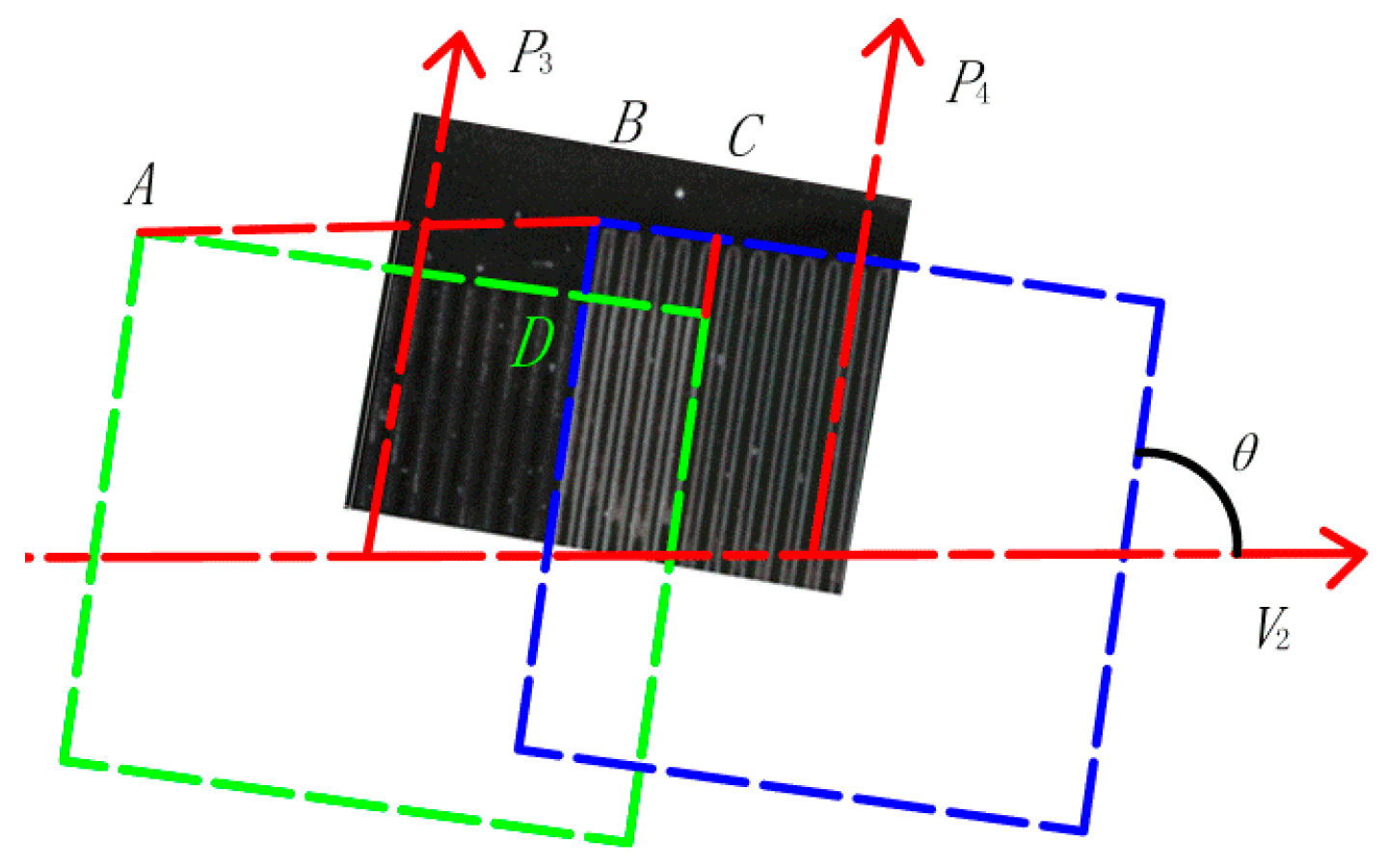
Figure 3.
Several grating imagines caused by the different angles: (a) Leaning to the left and overlap phenomenon, overlap value is BC/sinθ; (b) Leaning to the right and overlap phenomenon, overlap value is BC/sinθ; (c) Leaning to the left, and the interval distance value is BC/sinθ; (d) Leaning to the right, and the interval distance value is BC/sinθ.

Figure 4.
Tilting legend of Mask. (a) Grating defocused image; (b) The X-direction grayscale curve consistent with (a).
Figure 4.
Tilting legend of Mask. (a) Grating defocused image; (b) The X-direction grayscale curve consistent with (a).

Figure 5.
The detected image at different focal position. (a) SMD = 6.41; (b) SMD = 6.85; (c) SMD = 7.19; (d) SMD = 7.80; (e) SMD = 7.95; (f) SMD = 7.64; (g) SMD = 7.20; (h) SMD = 6.39.
Figure 5.
The detected image at different focal position. (a) SMD = 6.41; (b) SMD = 6.85; (c) SMD = 7.19; (d) SMD = 7.80; (e) SMD = 7.95; (f) SMD = 7.64; (g) SMD = 7.20; (h) SMD = 6.39.

Figure 6.
The principle of splicing lithography method.

Figure 7.
The third lithography after achieving precise alignment.

Figure 8.
Schematic diagram for the experimental setup.

Figure 9.
Grating lithography accuracy detection in 200 mm length.


Table 1.
Adjacent Pixel Gray Variance and Normalization.
| a | b | c | d | e | f | g | h | |
|---|---|---|---|---|---|---|---|---|
| 6.41 | 6.85 | 7.19 | 7.80 | 7.95 | 7.64 | 7.20 | 6.39 | |
| 0.01 | 0.29 | 0.51 | 0.91 | 1.00 | 0.80 | 0.52 | 0.00 |
Publisher’s Note: MDPI stays neutral with regard to jurisdictional claims in published maps and institutional affiliations. |
© 2017 by the authors. Licensee MDPI, Basel, Switzerland. This article is an open access article distributed under the terms and conditions of the Creative Commons Attribution (CC BY) license (https://creativecommons.org/licenses/by/4.0/).
Share and Cite
MDPI and ACS Style
Ren, D.; Xi, J.; Li, Z.; Li, B.; Zhao, Z.; Zhao, H.; Cui, L.; Xu, H. The Alignment Method for Linear Scale Projection Lithography Based on CCD Image Analysis. Proceedings 2018, 2, 101. https://doi.org/10.3390/ecsa-4-04936
AMA Style
Ren D, Xi J, Li Z, Li B, Zhao Z, Zhao H, Cui L, Xu H. The Alignment Method for Linear Scale Projection Lithography Based on CCD Image Analysis. Proceedings. 2018; 2(3):101. https://doi.org/10.3390/ecsa-4-04936
Chicago/Turabian StyleRen, Dongxu, Jianpu Xi, Zhengfeng Li, Bin Li, Zexiang Zhao, Huiying Zhao, Lujun Cui, and Hang Xu. 2018. "The Alignment Method for Linear Scale Projection Lithography Based on CCD Image Analysis" Proceedings 2, no. 3: 101. https://doi.org/10.3390/ecsa-4-04936