Assessment of Micromechanically-Induced Uncertainties in the Electromechanical Response of MEMS Devices †


Department of Civil and Environmental Engineering, Politecnico di Milano, Piazza L. da Vinci 32, 20133 Milan, Italy
*
Author to whom correspondence should be addressed.
†
Presented at the 3rd International Electronic Conference on Sensors and Applications, 15–30 November 2016; Available online: https://sciforum.net/conference/ecsa-3.
Proceedings 2017, 1(2), 39; https://doi.org/10.3390/ecsa-3-S1001
Published: 14 November 2016
(This article belongs to the Proceedings of Proceedings of the 3rd International Electronic Conference on Sensors and Applications, 15–30 November 2016; Available online: https://sciforum.net/conference/ecsa-3.)
Abstract
:Microelectromechanical systems (MEMS) have been already successfully commercialized for around 20 years. The design of novel MEMS sensors currently targets two important features: smaller dimensions and higher reliability. As the characteristic size of the mechanical components of the devices decreases, uncertainties in the mechanical and geometrical properties induced by the microfabrication process become more and more important. To address these issues, an on-chip testing device has been proposed to avoid any visual inspection for the read-out. The electromechanical responses of ten nominally identical specimens have been recorded, and experimental data have shown a significant scattering due to the presence of relevant uncertainty sources. To interpret the response of the device, an analytical reduced-order model of the whole device has been developed. A genetic algorithm has then been adopted to identify features of the mechanical and geometrical uncertainties in the batch of test structures.
1. Introduction
MEMS devices have become one of the successfully commercialized examples of micro and nano technology. Nevertheless, the constant demand for innovative devices has been leading engineers to move toward ever smaller devices. The miniaturization of the mechanical components may thus increase reliability issues related to the mechanical or geometrical properties of final fabricated devices. Therefore, improvement in our understanding of the effects of the involved uncertainties on the devices’ operational performance is always needed. Robust in-situ experimental techniques coupled with appropriate numerical tools is necessary to achieve this goal.
In this study, we exploit an on-chip testing device fabricated by standard MEMS fabrication technology [1] to assess the micromechanically-induced uncertainties in the response. In an earlier work [2], we attempted to explore the feasible range of uncertainties originated from the polysilicon film properties by taking into account the statistical variation of its Young’s modulus. Comparing the numerical studies and the experimental evidences, it was demonstrated that other sources of uncertainties must also be allowed for. To this aim, we introduce here other uncertainty sources and present an assessment of their variation in the specimens using an appropriate parameter estimation scheme.
In the following, we first discuss the most important details of the experimental campaign and of the model employed for an analytical interpretation of the data. Next, the parameter estimation procedure is explained and some pertinent results are finally discussed.
2. Experiment Design and Modelling
The devices developed for this work have been produced through the ThELMA process [1] by STMicroelectronics. SEM images of the whole structure and of some details of it are reported in Figure 1. The specimen undergoing deformations is a cantilever-like beam (see Figure 1b), which is connected to a fixed anchor at its top side. The micro beam is connected at the opposite side to a 200 m × 200 m plate denoted as rotor. The main geometrical characteristics of the tested device are summarized in Table 1.
Actuation and sensing are obtained using a standard electrostatic technique, by employing the stators around the rotor. By applying an electrical potential difference between the stator and the rotor, an attractive force will be generated to move the rotor towards the stator(s). Since the devices are capped, a visual investigation of the deformation of the device is not possible; therefore, the capacitance between the stators and the rotor can be measured and later transformed into the sought beam deformation through appropriate (either analytical or numerical) models. The resulting input-output relationship is then in the format of capacitance change versus actuation voltage, or C–V curve.
Two sets of stators have been devised for testing. One is located on the right side of the rotor (see Figure 1) and is called lateral capacitor. Other two stators are located on the top and bottom sides of the rotor are are electrically connected; they are called rotational capacitors as they only induce a rotation of the rotor due to their position. Thus, two alternative configurations are possible for actuation: by inducing a potential difference at the rotational capacitors (rotational actuation), or by inducing a potential difference at the lateral capacitor (lateral actuation). As for the capacitance measurement, two alternatives are similarly available. Therefore, the two sets of capacitors overall provide four different testing configurations.
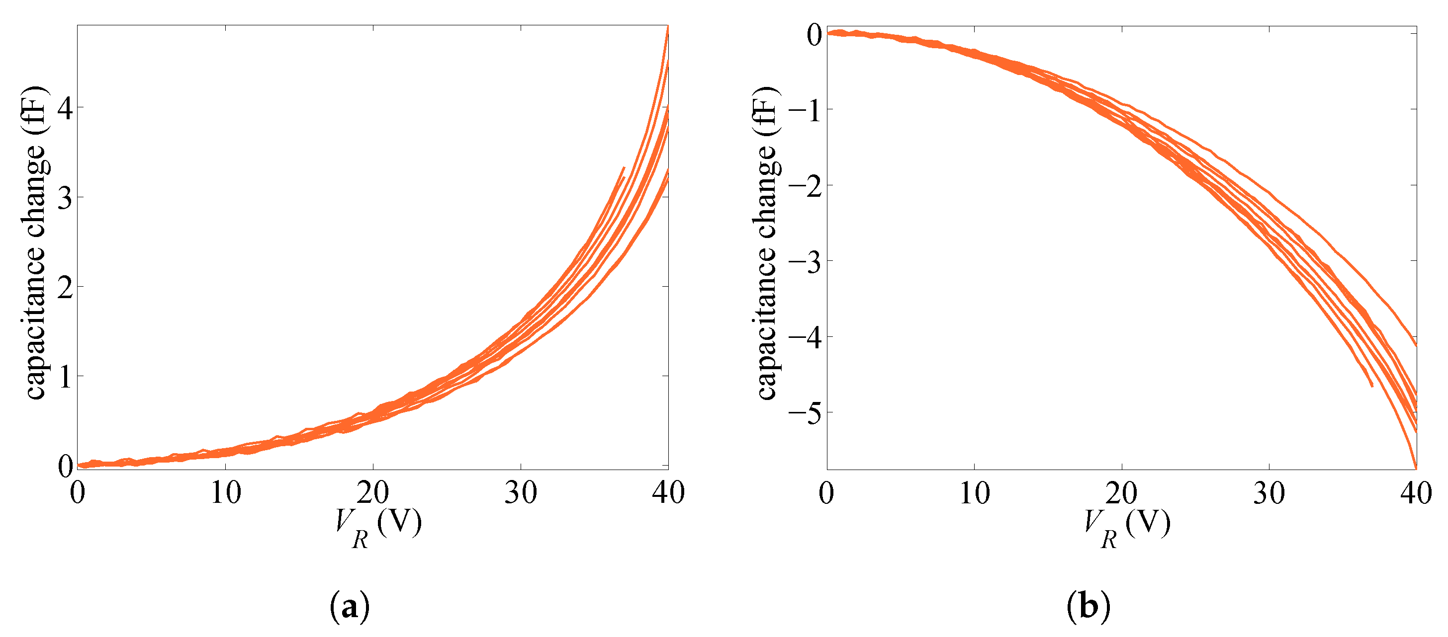
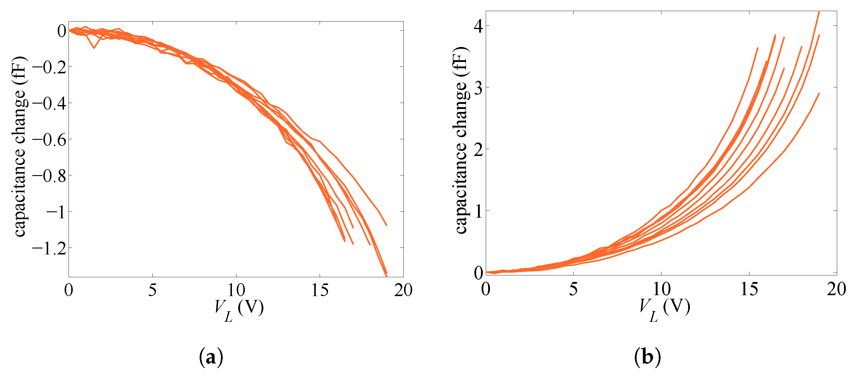
In what follows, we gather the results on the basis of the type of actuation: when the rotational capacitor is biased by voltage , and when the lateral capacitor is biased by voltage . Ten specimens are taken randomly from the same wafer. The responses of these ten different devices, in terms of change in the capacitance values at increasing applied voltage are reported in Figure 2 and Figure 3 for the rotational and lateral cases, respectively. The effects of measurement noise are shown at low actuation levels, but the measurement to error ratio improves as the level of actuation rises. The measured C–V curves show that the response of the devices is rather scattered. In [2,3], it was shown that such scattering cannot be linked to micromechanical features of the polysilicon film only; through a Monte Carlo analysis and finite element simulations of the coupled electro-mechanical response of the test structure, wherein the morphology of the polycrystalline silicon was appropriately handled, a by far less scattered response was foreseen. Hence, the different responses collected in the plots cannot be physically justified on purely mechanical grounds and must be therefore induced by (small) differences in the configuration of the capacitors too. Accordingly, both the geometric features and the homogenized material Young’s modulus of the microbeam are dealt with as stochastic variables in the forthcoming analysis.
In this work, we exploit a reduced-order model of the testing device developed in [3], where it was shown that the model is able to capture the principal behavior of the devices. The aforementioned uncertain parameters were the Young’s modulus E of the microcantilever and the overetch O. In [3], we also showed that the model needs to be further enhanced by considering other sources of uncertainties to better match the experimental data. In this regard, the next likely parameter to be considered is the initial offset displacement of the central rotor, which can heavily affect the system response and is prone to changes due to the fabrication process. This rotor displacement can be parameterized by an initial beam-end deflection , and an initial beam-end rotation . Between the two, the beam-end rotation is the prominent parameter. The effects of the initial offset for the rotational capacitors, both at actuation and sensing, is negligible. Since the admissible values for are small relatively to the gap distance (see Figure 1), such changes do not also alter the system behavior at the lateral capacitor accordingly . Therefore, in the following we take into account the rotation offset value only. Insertion of this parameter into the analytical model provided in [3] is carried out by a simple modification as .
Using the three unknown parameters, namely O, E and , the sensitivity of the response to these parameters is investigated first; for such purpose, one may observe the capacitance change corresponding to an arbitrary actuation voltage. The variation range of overetch and Young’s modulus are [−0.15 m, +0.15 m] and [130 GPa, 169 GPa], respectively. In order to have a physical understanding of the variation range of rotation offset, we have resorted to the pull-in instability configuration. In a separate analysis, the rotation angle corresponding to pull-in instability for rotational and lateral actuation have been obtained as −0.0088 and 0.0042 rad, respectively. These values are calculated using reference values for overetch and Young’s modulus, i.e., O = 0 m and E = 149.3 GPa. These values have to be compared to the minimum and maximum ones [ = −0.02 rad, = 0.01 rad], at which the vertices of rotor get in touch with the capacitor surfaces. Taking those calculations into account, the variation range for the offset has been set as [ = −0.004 rad, = 0.004 rad].
Figure 4 reports the developed capacitance change at the rotational capacitors when voltage difference = 37 V is applied at the same capacitance (RR case according to Figure 2). As it can be observed, all the three parameters effectively change the device response. In the case of overetch, the capacitance change varies in a strong nonlinear fashion, while the Young’s modulus and the rotation offset have a quasi linear effect.
3. Uncertainty Quantification through Genetic Algorithms
To estimate the most probable parameter values for each single device from the experimental C–V curves, a genetic algorithm (GA) have been adopted as a global optimization strategy [4]. The population size to explore the parameter space (design or search space) is an important factor determining the efficiency of the procedure [5,6]: adding more samples requires more function evaluations and thus, more computational effort. On the other hand, handling a big population generally has two advantages: an in-depth space search and therefore more probability of reaching the best possible set of parameter values; less number of generations required for the convergence of the algorithm.
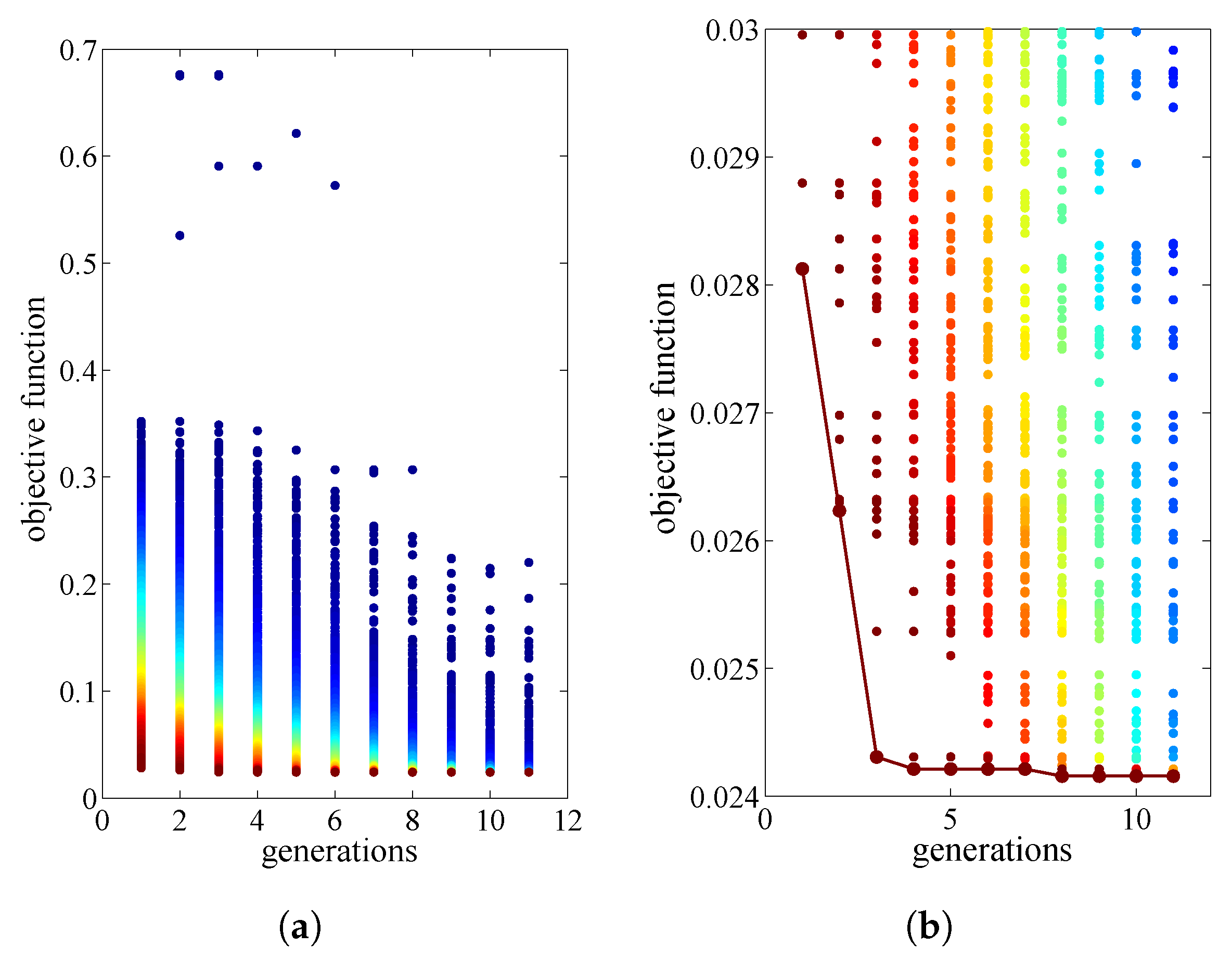
The same scheme of [3] has been also adopted in this analysis. Since the sought parameters are independent of the type of actuation, the parameter estimation procedure can be carried out for the two actuation types separately, to cross-validate the estimations. As for the objective function to be minimized by the GA, the normalized discrepancy between the measured capacitance and the model predictions has been recoursed to. Taking into account the three uncertain parameters O, E and ; a population of 5000 individuals and 11 generations have been finally adopted. Figure 5 shows the convergence of the GA in terms of the objective function value for the exemplary case of specimen #2; Figure 5b illustrates the close-up of the bottom part of Figure 5a, along with the trend of the best individual score. Each dot in the figure stands for the objective function value for one individual. The color is assigned so that dark blue stands for the individual which shows the largest objective function value, and dark red stands for the best individual at each generation (corresponding to the smaller objective function value). At the evaluation of first generation (random spread of individuals within the parameters space), the individuals show a wide range of values of the objective functions; as the generations advance, the individuals move to the bottom of the graph concentrating around the best possible solution. It can be observed that the rate of convergence is relatively high since the number of individuals is large; although the convergence of the algorithm occurs at the 8th generation, the fluctuation in the objective function after the 4th is quite negligible as for the best solution.
The parameter estimation procedure based on the GA has been carried out on each specimen; the relevant estimated parameters are reported in Table 2. The values are categorized under the two actuation types, and . These values can be compared to one another to cross-validate the procedure for each specimen. By inspecting the outcomes, it clearly emerges that the current identification attempt has provided better results than those reported in [3], featuring more consistency between the two sets of estimated values. The reason behind this improvement is linked to the third handled uncertain parameter, the rotation offset , which allows to model the scatterings in the initial configuration due to possible residual stress and/or stress gradient effects. Despite the improvement, there are still some specimen for which the method was not able to generate consistent results (e.g., specimens #4 and #6). More insights into the uncertainties can be obtained through further enhancements, using numerical models instead of the analytical ones. Numerical models, such as finite element ones, are supposed to provide better results as they can allow for additional uncertain parameters. On the other hand, the use of Bayesian tools is generally favorable in comparison to the deterministic approaches (such as the one adopted in this work) when the measurement errors have to be properly dealt with. These enhancements, within the frame of a complete uncertainty quantification scheme, are planned for future activities.
Author Contributions
The authors contributed equally to this work.
Acknowledgments
Financial support provided by STMicroelectronics through project MaRe (MAterial REliability) is gratefully acknowledged.
Conflicts of Interest
The authors declare no conflict of interest.
References
- Corigliano, A.; Cacchione, F.; De Masi, B.; Riva, C. On-chip electrostatically actuated bending tests for the mechanical characterization of polysilicon at the micro scale. Meccanica 2005, 40, 485–503. [Google Scholar] [CrossRef]
- Mirzazadeh, R.; Ghisi, A.; Mariani, S. Assessment of overetch and polysilicon film properties through on-chip tests. In Proceedings of the 2nd International Electronic Conference on Sensors and Applications, 15–30 November 2015; pp. 1–7. [Google Scholar]
- Mirzazadeh, R.; Eftekhar Azam, S.; Mariani, S. Micromechanical Characterization of polysilicon films through on-Chip tests. Sensors 2016, 16, 1191. [Google Scholar] [CrossRef] [PubMed]
- Patelli, E.; Alvarez, D.; Broggi, M.; De Angelis, M. Uncertainty management in multidisciplinary design of critical safety systems. J. Aerosp. Inf. Syst. 2014, 12, 140–169. [Google Scholar] [CrossRef]
- Chen, S.; Montgomery, J.; Bolufé-Röhler, A. Measuring the curse of dimensionality and its effects on particle swarm optimization and differential evolution. Appl. Intelli. 2015, 42, 514–526. [Google Scholar] [CrossRef]
- Chen, T.; Tang, K.; Chen, G.; Yao, X. A large population size can be unhelpful in evolutionary algorithms. Theor. Comput. Sci. 2012, 463, 54–70. [Google Scholar] [CrossRef]
Figure 1.
SEM images showing (a) the whole device geometry, and details (b) of the beam and (c) in proximity of the lateral/bottom stators.
Figure 1.
SEM images showing (a) the whole device geometry, and details (b) of the beam and (c) in proximity of the lateral/bottom stators.

Figure 2.
Experimental results with rotational actuation: (a) RR case (rotational actuation, rotational sensing); (b) RL case (rotational actuation and sensing).
Figure 2.
Experimental results with rotational actuation: (a) RR case (rotational actuation, rotational sensing); (b) RL case (rotational actuation and sensing).

Figure 3.
Experimental results lateral actuation: (a) LR case (lateral actuation, rotational sensing); (b) LL case ( lateral actuation and sensing).
Figure 3.
Experimental results lateral actuation: (a) LR case (lateral actuation, rotational sensing); (b) LL case ( lateral actuation and sensing).

Figure 4.
RR case, = 37 V: sensitivity of the device response to (a) overetch O; (b) Young’s modulus E; and (c) offset .
Figure 4.
RR case, = 37 V: sensitivity of the device response to (a) overetch O; (b) Young’s modulus E; and (c) offset .

Figure 5.
(a) Convergence of the objective discrepancy function at increasing generations; and (b) close-up of the plot and best score trend.
Figure 5.
(a) Convergence of the objective discrepancy function at increasing generations; and (b) close-up of the plot and best score trend.


Table 1.
Geometric dimensions of the device.
| Parameter | Value | Parameter | Value |
|---|---|---|---|
| beam length (l) | 20 m | initial gap at capacitors () | 2 m |
| beam width (h) | 2 m | a | 17 m |
| out-of-plane film thickness (w) | 22 m | L | 200 m |
Table 2.
Estimated parameter values.
| O (m) | (Milliradian) | E (GPa) | ||||||
|---|---|---|---|---|---|---|---|---|
| Specimen # | through | through | through | through | through | through | ||
| 1 | −0.10 | −0.05 | 0.08 | 0.34 | 134.6 | 131.6 | ||
| 2 | −0.09 | −0.02 | −0.15 | 0.07 | 147.6 | 137.7 | ||
| 3 | −0.09 | −0.13 | −0.31 | −0.30 | 150.8 | 153.2 | ||
| 4 | −0.12 | −0.07 | −0.01 | −0.05 | 149.5 | 130.7 | ||
| 5 | −0.09 | −0.10 | −0.55 | −0.56 | 149.5 | 141.8 | ||
| 6 | −0.07 | −0.07 | −0.42 | −0.85 | 161.5 | 144.2 | ||
| 7 | −0.10 | −0.10 | 0.07 | 0.41 | 130.3 | 134.3 | ||
| 8 | −0.12 | −0.06 | 0.12 | 0.46 | 134.0 | 130.2 | ||
| 9 | −0.04 | −0.05 | 0.91 | 1.00 | 131.1 | 135.5 | ||
| 10 | −0.06 | −0.12 | 0.52 | 0.53 | 132.2 | 142.6 | ||
Publisher’s Note: MDPI stays neutral with regard to jurisdictional claims in published maps and institutional affiliations. |
© 2016 by the authors. Licensee MDPI, Basel, Switzerland. This article is an open access article distributed under the terms and conditions of the Creative Commons Attribution (CC BY) license (https://creativecommons.org/licenses/by/4.0/).
Share and Cite
MDPI and ACS Style
Mirzazadeh, R.; Mariani, S. Assessment of Micromechanically-Induced Uncertainties in the Electromechanical Response of MEMS Devices. Proceedings 2017, 1, 39. https://doi.org/10.3390/ecsa-3-S1001
AMA Style
Mirzazadeh R, Mariani S. Assessment of Micromechanically-Induced Uncertainties in the Electromechanical Response of MEMS Devices. Proceedings. 2017; 1(2):39. https://doi.org/10.3390/ecsa-3-S1001
Chicago/Turabian StyleMirzazadeh, Ramin, and Stefano Mariani. 2017. "Assessment of Micromechanically-Induced Uncertainties in the Electromechanical Response of MEMS Devices" Proceedings 1, no. 2: 39. https://doi.org/10.3390/ecsa-3-S1001