Article

Proximity-Induced Superconducting States of Magnetically Doped 3D Topological Insulators with High Bulk Insulation

1
Department of Applied Physics, Nagoya University, Furo-cho, Chikusa-ku, Nagoya 464-8603, Japan
2
Laboratory for Materials and Structures, Tokyo Institute of Technology, Yokohama 226-8503, Japan
3
National Institute of Advanced Industrial Science and Technology (AIST), Tsukuba 305-8568, Japan
*
Author to whom correspondence should be addressed.
Current address: National Institute for Materials Science (NIMS), Tsukuba, Ibaraki 305-0003, Japan.
Condens. Matter 2019, 4(1), 9; https://doi.org/10.3390/condmat4010009
Submission received: 25 November 2018 / Revised: 22 December 2018 / Accepted: 7 January 2019 / Published: 12 January 2019
(This article belongs to the Special Issue Majorana Fermions and Topological Materials Science)

Abstract

:
We studied magnetized topological insulator/superconductor junctions with the expectation of unconventional superconductive states holding Majorana fermions induced by superconductive proximity effects on the surface states of magnetized topological insulators (TIs), attached by conventional superconductors. We introduced Fe-doped BiSbTe2Se as an ideal magnetic TI and used the developed junction fabrication process to access the proximity-induced surface superconducting states. The bulk single crystals of the Fe-doped TI showed excellent bulk-insulating properties and ferromagnetism simultaneously at a low temperature. Meanwhile, the fabricated junctions also showed an insulating behavior above 100 K, as well as metallic conduction at a low temperature, which reflects bulk carrier freezing. In addition, we observed a proximity-induced gap structure in the conductance spectra. These results indicate that the junctions using the established materials and process are preferable to observe unconventional superconducting states which are induced via the surface channels of the magnetized TI. We believe that the developed process can be applied for the fabrication of complicated junctions and suites for braiding operations.

1. Introduction

Unconventional superconductive states hosting non-Abelian anyons [1,2,3], including Majorana fermions [4] on their surface Andreev bound states [5,6,7], are indispensable constituents for future fault-tolerant quantum computing [8,9]. In principle, superconductive proximity-induced states with strong spin-orbit coupling (SOC) and magnetic fields emulate topological superconductors and odd-frequency superconductors [7,10,11]. Indeed, signatures of Majorana fermions have been observed in Rashba nanowires [12,13,14] and two-dimensional (2D) topological insulator (TI)-based junctions [15,16]. These induced superconductive states are expected to have p-wave symmetry as a gap function Δ [2,11]. In three-dimensional (3D) TI-based junctions, although the origins of zero-bias conduction peaks are still controversial due to the existing bulk carriers [17], such signals are considered to also represent the p-wave superconductivity states [18,19]. Furthermore, the 3D TI-based junctions potentially induce further unconventional superconductivity states, which provide another possible way to access Majorana fermions; the proximity-induced superconductive states depend on the strength and direction of the applied magnetic fields and moments [20,21,22,23].
Recently, we reported the observation of an unconventional proximity effect on an Fe-doped Bi2Te2Se (Fe-BTS)-based Josephson junction [24]. The differential conductance spectra showed an unusual three-peak structure with a tiny peak width (~6 μeV) around a zero-bias voltage. One particularly notable signature was the 4π-periodic Josephson supercurrent under high-power radio-frequency irradiation, which implied the existence of peculiar surface Andreev bound states. However, it was difficult to identify the symmetries of Cooper pairs induced on the junction, due to the complicated conductance spectra, which were possibly derived from the coexistence of several conductance channels: (i) the 2D surface states of magnetic TI; (ii) the 1D edge channel which emerged at the edge of the crystal flakes; and (iii) bulk conduction. Establishing ideal junctions without the contributions of the 1D edge channel and bulk conduction is crucial to observing the proximity effect through the surface states of magnetic TI.
Regarding the contribution of the 1D edge channel, we have to develop a new junction fabrication process avoiding electrical contacts between the electrodes and crystal edges of crystal flakes. As for the contribution of bulk conduction, on the other hand, reducing the number of bulk carriers of the magnetic TIs is essential. The junctions of the Fe-doped Bi2Te2Se were found to exhibit n-type conduction with metallic resistivity (several mΩcm, calculated from reference [24]), whereas non-doped Bi2Te2Se bulk crystals have been reported to have large bulk resistivity [25,26,27] (the carrier type depended on the small amount of composition fluctuation [25,28]). This comparison implies that Fe-substitution acted with electron-doping characteristics. Therefore, in our strategy for achieving a high bulk-insulating nature of magnetized TIs, we focused on the p-type semiconductor BiSbTe2Se [29], and attempted Fe-substitution in the (Bi, Sb) sites.
In this paper, we successfully grew new magnetized TI single crystals with excellent bulk-insulating properties and report a newly developed fabrication process to avoid electrical contacts between electrodes and the crystal edges of the grown crystal flakes (the contribution of the 1D edge channel). As a result, we confirmed the emergence of a proximity effect through the surface states on the grown magnetic TIs. We believe that the established experimental technique and samples will reveal the predicted unusual unique superconductive states on the magnetic TI-based junctions.

2. Results and Discussion

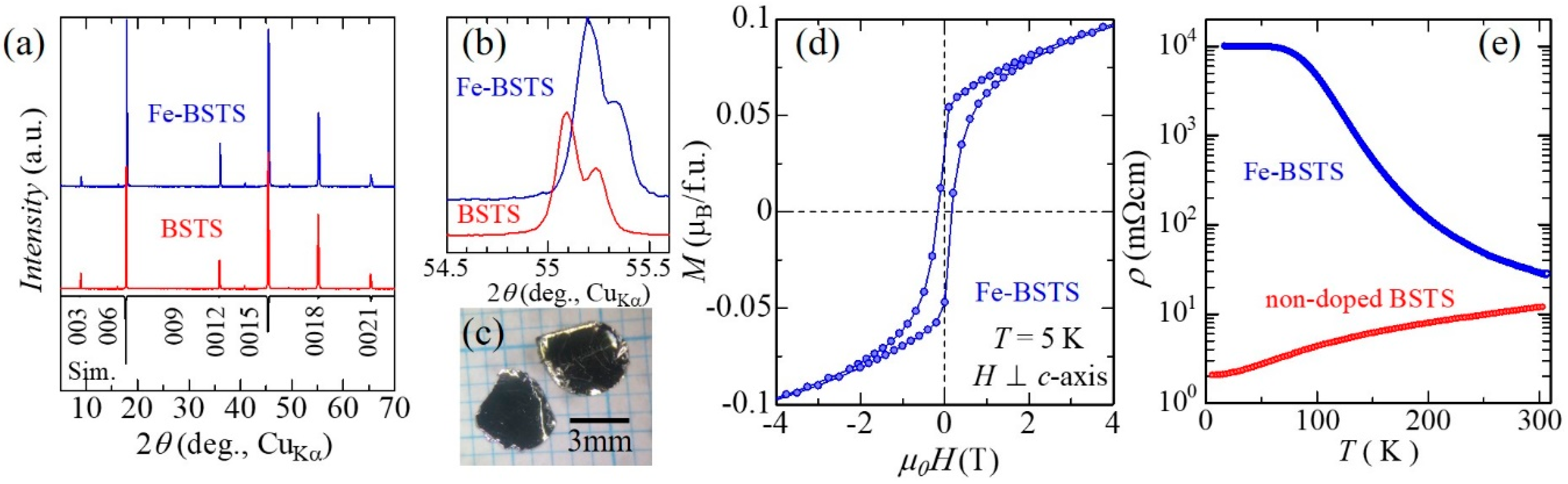
2.1. Crystal Growth and Characterization

In this section, we present the sample quality, chemical composition, and magnetism of single crystals of Fe-doped BiSbTe2Se (Fe-BSTS) and then show the transport properties of the crystals.
Grown bulk single crystals of Fe-BSTS can be easily cleaved at the (0 0 l) planes (Figure 1c). The X-ray diffraction (XRD) from the cleaved planes showed only clear sharp 00l peaks (Figure 1a). The small peaks at slightly lower angles before the high-intensity peaks (e.g., ~40° and 50°) corresponded to reflections of the 00l peaks from the weak Cu contributions. Higher angle peaks showed clear Cu1-Cu2 peak splitting, with slight peak broadening compared with non-doped BiSbTe2Se (BSTS), ensuring good crystalline quality (Figure 1b). The slight peak shift toward higher angles by the doping indicates lattice shrinking. Indeed, the lattice parameter c of Fe-BSTS was c = 29.96 Å and was slightly smaller than that of BSTS [30], reflecting substitution with smaller atoms of Fe for larger (Bi, Sb) sites. In addition, we also tested the powder XRD measurements of the ground crystal flakes and confirmed that no extra impurity phase was detected. To determine the Fe concentration and distribution of the obtained crystals, we conducted X-ray fluorescence analysis (XRF) to the crystals after the XRD measurements. The typical analytical Fe composition was ~0.01, and this Fe distribution of crystal flakes, at several mm2, was almost homogeneous within the analytical accuracy of XRF. Figure 1d shows the magnetization of the crystals measured at 5 K and indicates ferromagnetism with a narrow hysteresis loop. The saturation magnetization was around 0.065 μB per formula unit. This value can be understood by considering the analytical chemical composition and a possible ionic state of high-spin Fe3+ (5 μB). Therefore, these results indicate that the ferromagnetism observed here is caused by Fe doping in the BSTS, establishing a ferromagnetic TI. Owing to the time-inversion symmetry induced by the ferromagnetism, a gap opening at the Dirac point—i.e., a massive Dirac cone state—should be realized as well, as in [31].
The temperature dependence of the in-plane resistivity of Fe-doped and non-doped BSTS was examined (Figure 1e). The metallic temperature dependence of BSTS was drastically changed into insulator-like dependence by Fe doping. The most notable feature from the resistivity was the high bulk-insulating nature of the Fe-BSTS crystals. The resistivity reached ~10 Ωcm at 5 K and the thermal activation energy Ea was 79 meV above 150 K. The carrier density, evaluated from the standard Hall measurement, was n < 1.6 × 1016 cm−3 at 15 K. These properties are comparable with TIs with the highest insulating properties among Bi–Sb–Te–Se compounds; e.g., BiSbTeSe2 (ρ2K = 4 Ωcm, n2K ~ 1015 cm−3, Ea = 60–80 meV [32]) and Bi1.46Sb0.54Te1.7Se1.3 (ρ4K = 12.6 Ωcm, n4K = 0.2 × 1016 cm−3, Ea = 102 meV [33]). However, the resistivity of the Fe-BSTS at a low temperature became saturated and changed into metallic temperature dependence below 50 K, reflecting the surface metallic channels, as widely observed for surface-dominant TIs [26,27,32,33,34]. This implies that the Fermi level is located at the surface metallic states (out of the opened Dirac gap). Thus, the present material, Fe-BSTS, is expected to have unique surface states; i.e., a massive Dirac cone.
The effects of Fe and Sb substitution for the Bi sites were also confirmed by Seebeck coefficients. In general, the majority carrier type corresponds to the sign of the Seebeck coefficient, and its absolute value inversely depends on the carrier concentration, according to the Mott expression [35]. Seebeck coefficients of Fe-BSTS, non-doped BSTS, and Fe-BTS were found to be ~+500, +380, and −350 μV/K at 300 K, respectively. The majority carrier types of Fe-BSTS and BSTS crystals were p-type, while Fe-BTS were n-type. The larger value of Fe-BSTS than of BSTS reflects its good bulk-insulating nature, which indicates that carriers were compensated by the electron-doping accompanied by the Fe substitution. However, comparison with Fe-BTS indicates that Sb substitution worked as with hole-doping. As a result, the co-substitution in Bi sites realized excellent bulk carrier compensation, as per our strategy. Furthermore, the p-type conduction and the resistivity behavior indicate that the Fermi level is located at the surface states slightly below the Dirac gap. This situation is favorable for pursuing the unusual transport nature of the massive Dirac cones. Considering the Dirac points close to the valence band in the Bi–Sb–Te–Se compounds [31,33,34], slight carrier tuning by the back-gating or the electrical double layer technique [36] can easily tune the Fermi level into or out of the opened gap of magnetic TIs. Therefore, these results indicate that Fe-BSTS has a desirable nature for observing such unique surface states.

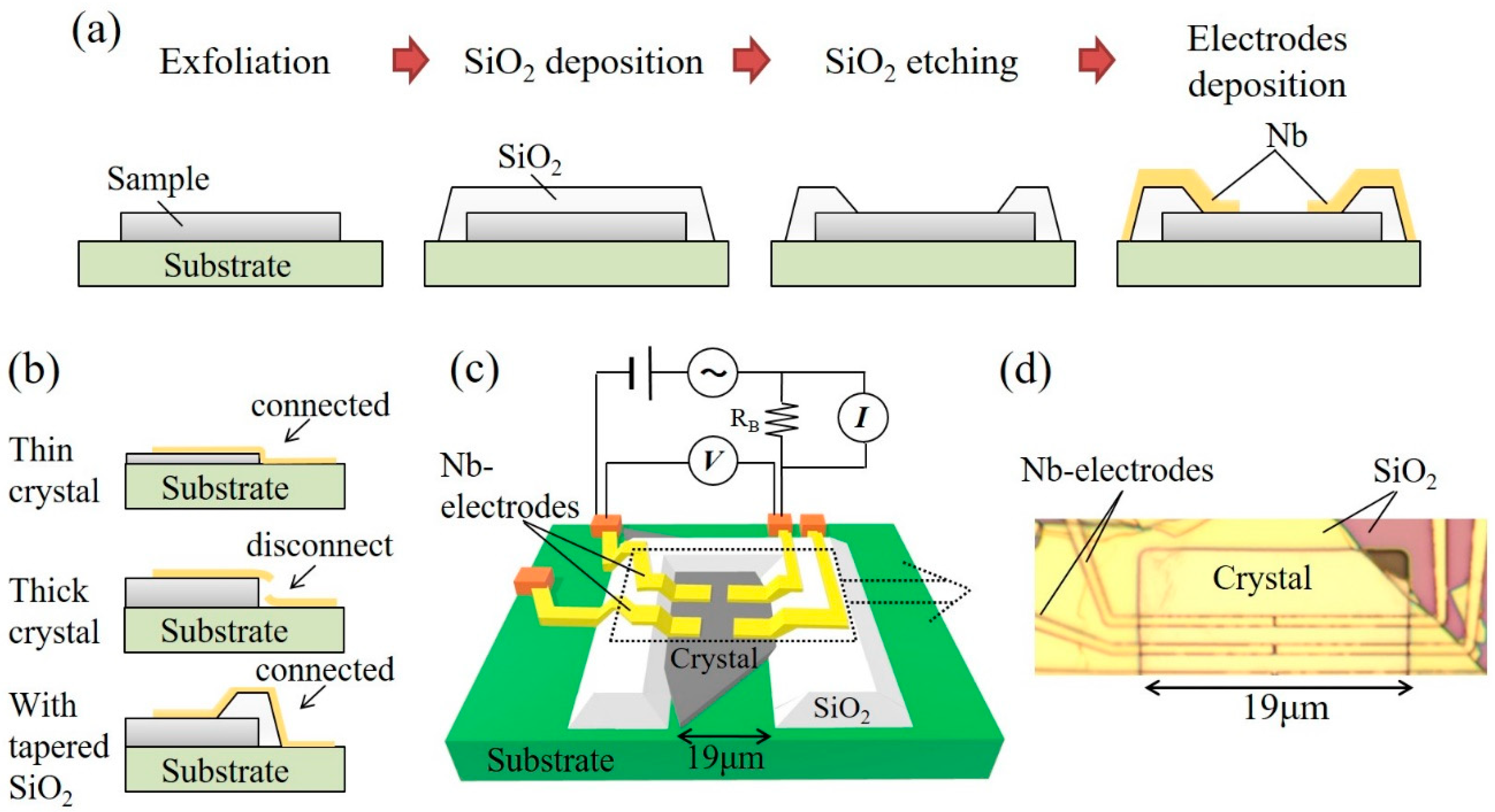
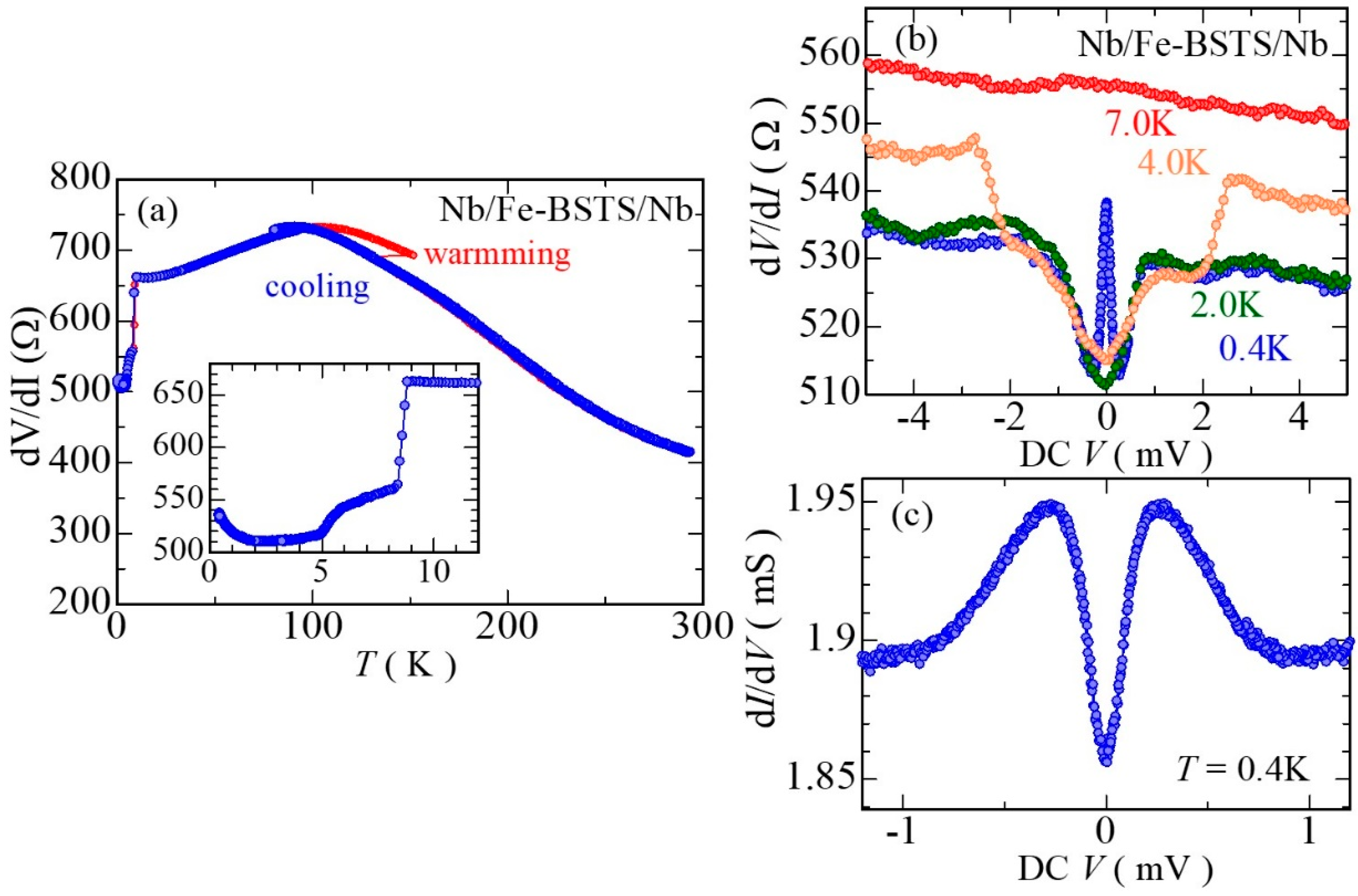
2.2. Junction Fabrication and Transport Properties

The conventional semiconductor fabrication technique was applied in the fabrication procedure. Figure 2a summarizes the developed procedure. First, the crystal flakes were repeatedly exfoliated by using Scotch tapes to achieve the desired sample thickness. The flakes were then transferred onto a Si substrate. In the standard process, electrodes are placed directly on the flakes using the appropriate techniques, such as e-beam and/or spattering. In that situation, the electrodes cannot avoid contact with the crystal edge where 1D edge channels may exist. Considering the deposition of electrodes on the thick samples, electrical disconnection may easily occur at the sample edge (Figure 2b). Instead, we performed SiO2 deposition with a thin insulating buffer layer as the second step. Note that to prevent the thermal oxidation of the chalcogenide samples during the SiO2 deposition, the deposition temperature was tuned to low, and a thin buffer layer was located at the top of the samples to prevent direct exposure to plasma. In the third step, SiO2 etching was performed on an appropriated sample area by standard reactive ion etching (RIE) by using CHF3 gases. This etching was carefully finished when it entered the buffer layer. The remaining buffer was removed by wet chemical etching. The final step was the deposition of electrodes. During the whole process, sample flakes were not directly exposed to the oxidation atmosphere and the strong acids/alkalis that may have damaged the crystals. By applying this procedure to Fe-BSTS, we can access surface-dominant transport without 1D edge channels.
One additional benefit of this process is that we can easily achieve good electrical contact even for thick crystals due to the naturally tapered shape of SiO2 formed during SiO2 deposition and RIE etching (see schematic picture in Figure 2b). To obtain good side-wall coverage, electrode deposition is usually conducted with substantial angles, as adopted by Stehno and colleagues [37]. However, our fabrication procedure does not require these techniques.
As a preliminary test to check the emergence of a supercurrent through a surface conduction state, we fabricated Nb/Fe-BSTS/Nb junctions (Figure 2c). The optical micrograph is shown in Figure 2d. The Nb-electrodes with Ti buffer layers were made by the sputtering technique. All fabricated junctions had good electrical contact without disconnection at the crystal edges. The designed electrode width was ~1 μm.
The transport properties of Nb/Fe-BSTS/Nb junctions were measured by the standard lock-in technique. A simplified circuit is depicted in Figure 2c. The temperature dependence of the zero-bias differential resistance showed insulator-like behavior above 100 K, while it was metallic at a low temperature (Figure 3a). This was reflected in the nature of single crystal transport, and the surface-dominant nature also emerged in the junctions. The value of resistance is comparable with the sum of bulk resistance evaluated from the resistivity and estimated contact resistance, ensuring that crystal flakes were not significantly damaged during the developed process. A clear resistance drop was observed at 8.7 K, which corresponds to the superconductive transition temperature of the Nb electrodes. An additional slight resistance drop was found at around 5 K. Comparing the dynamic resistance spectra measured at 7.0 K and 4.0 K (Figure 3b), a gap-like structure was shown to form at around 5 K. The resistance for a bias voltage greater than 2 mV gradually decreased with temperature. This may reflect the temperature dependence of the resistivity of the crystal flake, suggesting that both the two zero-bias resistance drops came from the Nb electrodes. Such a two-step drop is widely observed on Nb-based superconductive junctions, including our previous result [24]. The unique proximity effect possibly started to develop around 2 K (=Tc,prox) where the resistance became increased. At the lowest temperature of 0.4 K, no signature of the Josephson supercurrent was observed. This indicates that the junction behaves as a serially connected S/N junction instead of an S/N/S tunnel or Josephson junctions (S: superconductor, N: normal metal), which allows us to evaluate the density of the states of quasiparticles by differential conductance measurement. Figure 3c shows the conductance spectra of the junctions at 0.4 K. The clear conduction dip structure was confirmed. Usually, the conventional S/N junctions show a U-shaped dip, reflecting the conventional superconductivity states [38]. However, the observed spectra resembled a V-shape.
Similar V-shape dips have been reported in other TI/superconductor (TI/S) junctions [39,40], while the zero-bias conductance peaks have been also detected in TI/S junctions [17,37,41]. As mentioned in the introduction, TI/S junctions are expected to behave as a p-wave superconductor, and both the dip and the peak in the spectra possibly reflect this p-wave nature. According to the theoretical calculation [6,42,43], the spectra of p-wave superconductors drastically change from the peak signals into the dip-like structure, depending on the effective barrier strength Z, and sharp signals at T = 0 K are dulled at finite temperature. This indicates that to discuss spectra shape, we have to consider contact states between TI/S junctions. In the present junction, the observed spectra at T = 0.4 K are quite similar with that of a nodal p-wave superconductor/normal metal junction with the parameters of Z = 2.0 and T = 0.2 Tc [43]. Considering the present situations (TI/S junction without insulating layers and Tc = Tc,prox ~ 2 K), these assumed parameters are reasonable. Thus, as one possible scenario, the nodal p-wave superconductive state may emerge on the Nb/Fe-BSTS/Nb junctions.
The origin of the p-wave nature, on the other hand, is not easily understood because of the existence of strong spin-orbit coupling and magnetic moments in Fe-BSTS. The pair symmetry and its amplitude are strongly dependent on the direction of magnetic moments and junction setups [22]. Indeed, ferromagnet/S junctions on TI [44] and TI ferromagnet/p-wave S junctions [45] are expected to induce different symmetry classes and amplitudes, while both differential conductance spectra are similar with the present case. To identify the pair symmetry, detailed experimental investigations are indispensable. In particular, spectral measurements under a magnetic field with arbitrary direction are promising. Even though we have to check the emergent superconducting states in the near future, the differential conductance spectra indicate that an unusual proximity effect is induced on the Nb/Fe-BSTS/Nb junctions, and the emergence of such an unconventional proximity effect is consistent with surface-dominant proximity effects. To observe concrete evidence of an unusual superconducting nature, we plan to investigate Fe-BSTS-based junctions and will pursue unobserved non-Abelian quasiparticles.

3. Materials and Methods

The single crystals of Fe-BSTS were grown by a modified Bridgman method similar to the case for Fe-BTS [24] and Fe- and Mn-doped Bi2Se3 single crystals [31]. The starting material composition was Fe:Bi:Sb:Te:Se = 0.1:0.95:0.95:2:1, and the appropriated amount of high purity elements was loaded into an evacuated quartz tube with a long, sharp-pointed bottom. The homogeneously melted samples achieved by the method described by Chen et al. [31] were slowly cooled down to 200 °C, and then rapid water quenching was performed. Sample characterization was performed by a conventional XRD measurement using Cu (D2 PHASER powder diffractometer with LynxExe 1D detector; Bruker, Billerica, MA, USA), and XRF analysis with XGT-5000 (HORIBA: Kyoto, Japan). Magnetization was confirmed using a commercial SQUID magnetometer (MPMS-XL: Quantum Design, San Diego, CA, USA). The resistivity, Seebeck coefficient and Hall coefficient of grown bulk crystals were analyzed with a homemade apparatus with a closed-cycle refrigerator equipped with a superconducting electromagnet.
The junction fabrication process was described in the text in detail. These procedures were performed at National Institute of Advanced Industrial Science and Technology (AIST) and National Institute for Materials Science (NIMS). The transport properties of the fabricated junctions were investigated by a standard lock-in technique with a modulation frequency of 961.1 Hz.

4. Conclusions

To establish the proximity effect through the surface-dominant channels of magnetic TIs, we prepared Fe-BSTS bulk single crystals and developed a fabrication process to avoid contact with the 1D edge channels. The Fe-BSTS bulk crystals had an excellent bulk-insulating nature, which reached 10 Ωcm at low temperatures. The Nb/Fe-BSTS/Nb junctions also showed a surface-dominant transport nature, and the emergence of a superconducting proximity effect was confirmed. These results imply that the junctions based on the Fe-BSTS fabricated by the developed process are promising systems for observing the unconventional proximity effects which are expected to emerge on the magnetic TIs.

Author Contributions

Conceptualization, T.S. and S.K.; Crystal Growth, H.T.H., S.Y. and M.K.; Junction Fabrication, K.T., M.K. and H.K.; Data Curation of Crystals, H.T.H.; Data Curation of Junctions, R.Y.; Writing-Original Draft Preparation, R.Y.; Writing-Review & Editing, all co-authors; Supervision, S.K.; Project Administration, S.K.; Funding Acquisition, T.S. and S.K.

Funding

This research was funded by JST CREST: grant no. JPMJCR16F2 and KAKENHI: grant nos. JP15H05851, 15H05853, 16H03847, 17K05485 and 18H01243.

Acknowledgments

The fabrication process was performed using the NIMS Nanofabrication Platform and AIST Nano-Processing Facility in the “Nanotechnology Platform Project” sponsored by the Ministry of Education, Culture, Sports, Science and Technology (MEXT), Japan.

Conflicts of Interest

The authors declare no conflict of interest.

References

  1. Sato, M.; Fujimoto, S. Majorana fermions and topology in superconductors. J. Phys. Soc. Jpn. 2016, 85, 1–32. [Google Scholar] [CrossRef]
  2. Fu, L.; Kane, C.L. Superconducting proximity effect and majorana fermions at the surface of a topological insulator. Phys. Rev. Lett. 2008, 100, 096407. [Google Scholar] [CrossRef] [PubMed]
  3. Linder, J.; Tanaka, Y.; Yokoyama, T.; Sudbø, A.; Nagaosa, N. Unconventional superconductivity on a topological insulator. Phys. Rev. Lett. 2010, 104, 067001. [Google Scholar] [CrossRef] [PubMed]
  4. Majorana, E.; Maiani, L. A symmetric theory of electrons and positrons. Ettore Majorana Sci. Pap. 2006, 201–233. [Google Scholar] [CrossRef]
  5. Kashiwaya, S.; Kashiwaya, H.; Saitoh, K.; Mawatari, Y.; Tanaka, Y. Tunneling spectroscopy of topological superconductors. Phys. E Low-Dimens. Syst. Nanostruct. 2014, 55, 25–29. [Google Scholar] [CrossRef] [Green Version]
  6. Kashiwaya, S.; Tanaka, Y. Tunnelling effects on surface bound states in unconventional superconductors. Rep. Prog. Phys. 2000, 63, 1641–1724. [Google Scholar] [CrossRef]
  7. Tanaka, Y.; Sato, M.; Nagaosa, N. Symmetry and topology in superconductors—Odd-frequency pairing and edge states. J. Phys. Soc. Jpn. 2012, 81, 011013. [Google Scholar] [CrossRef]
  8. Kitaev, A. Anyons in an exactly solved model and beyond. Ann. Phys. (N. Y.) 2006, 321, 2–111. [Google Scholar] [CrossRef] [Green Version]
  9. Nayak, C.; Simon, S.H.; Stern, A.; Freedman, M.; Das Sarma, S. Non-Abelian anyons and topological quantum computation. Rev. Mod. Phys. 2008, 80, 1083–1159. [Google Scholar] [CrossRef] [Green Version]
  10. Alicea, J. New directions in the pursuit of Majorana fermions in solid state systems. Rep. Prog. Phys. 2012, 75, 076501. [Google Scholar] [CrossRef] [Green Version]
  11. Beenakker, C.W.J. Search for Majorana fermions in superconductors. Annu. Rev. Condens. Matter Phys. 2011, 4, 113–136. [Google Scholar] [CrossRef]
  12. Das, A.; Ronen, Y.; Most, Y.; Oreg, Y.; Heiblum, M.; Shtrikman, H. Zero-bias peaks and splitting in an Al-InAs nanowire topological superconductor as a signature of Majorana fermions. Nat. Phys. 2012, 8, 887–895. [Google Scholar] [CrossRef]
  13. Rokhinson, L.P.; Liu, X.; Furdyna, J.K. The fractional a.c. Josephson effect in a semiconductor-superconductor nanowire as a signature of Majorana particles. Nat. Phys. 2012, 8, 795–799. [Google Scholar] [CrossRef]
  14. Mourik, V.; Zuo, K.; Frolov, S.M.; Plissard, S.R.; Bakkers, E.P.A.M.; Kouwenhoven, L.P. Signatures of Majorana Fermions in Hybrid Superconductor-Semiconductor Nanowire Devices. Science 2012, 336, 1003–1007. [Google Scholar] [CrossRef] [PubMed] [Green Version]
  15. Bocquillon, E.; Deacon, R.S.; Wiedenmann, J.; Leubner, P.; Klapwijk, T.M.; Brüne, C.; Ishibashi, K.; Buhmann, H.; Molenkamp, L.W. Gapless Andreev bound states in the quantum spin Hall insulator HgTe. Nat. Nanotechnol. 2017, 12, 137–143. [Google Scholar] [CrossRef] [PubMed]
  16. Wiedenmann, J.; Bocquillon, E.; Deacon, R.S.; Hartinger, S.; Herrmann, O.; Klapwijk, T.M.; Maier, L.; Ames, C.; Brüne, C.; Gould, C.; et al. 4π-periodic Josephson supercurrent in HgTe-based topological Josephson junctions. Nat. Commun. 2016, 7, 10303. [Google Scholar] [CrossRef] [PubMed] [Green Version]
  17. Li, H.; Zhou, T.; He, J.; Wang, H.W.; Zhang, H.; Liu, H.C.; Yi, Y.; Wu, C.; Law, K.T.; He, H.; et al. Origin of bias-independent conductance plateaus and zero-bias conductance peaks in Bi2Se3/NbSe2 hybrid structures. Phys. Rev. B 2017, 96, 075107. [Google Scholar] [CrossRef]
  18. Xu, J.P.; Wang, M.X.; Liu, Z.L.; Ge, J.F.; Yang, X.; Liu, C.; Xu, Z.A.; Guan, D.; Gao, C.L.; Qian, D.; et al. Experimental detection of a Majorana mode in the core of a magnetic vortex inside a topological insulator-superconductor Bi2Te3/NbSe2 heterostructure. Phys. Rev. Lett. 2015, 114, 017001. [Google Scholar] [CrossRef]
  19. Charpentier, S.; Galletti, L.; Kunakova, G.; Arpaia, R.; Song, Y.; Baghdadi, R.; Wang, S.M.; Kalaboukhov, A.; Olsson, E.; Tafuri, F.; et al. Induced unconventional superconductivity on the surface states of Bi2Te3 topological insulator. Nat. Commun. 2017, 8, 6–13. [Google Scholar] [CrossRef]
  20. Tanaka, Y.; Yokoyama, T.; Nagaosa, N. Manipulation of the Majorana Fermion, Andreev Reflection, and Josephson Current on Topological Insulators. Phys. Rev. Lett. 2009, 103, 107002. [Google Scholar] [CrossRef] [Green Version]
  21. Yokoyama, T. Josephson and proximity effects on the surface of a topological insulator. Phys. Rev. B 2012, 86, 075410. [Google Scholar] [CrossRef]
  22. Burset, P.; Lu, B.; Tkachov, G.; Tanaka, Y.; Hankiewicz, E.M. Superconducting proximity effect in three-dimensional topological insulators in the presence of a magnetic field. Phys. Rev. B 2015, 92, 205424. [Google Scholar] [CrossRef] [Green Version]
  23. Park, M.J.; Yang, J.; Kim, Y.; Gilbert, M.J. Fulde-Ferrell states in inverse proximity-coupled magnetically doped topological heterostructures. Phys. Rev. B 2017, 96, 064518. [Google Scholar] [CrossRef]
  24. Yano, R.; Koyanagi, M.; Kashiwaya, H.; Tsumura, K.; Hirose, H.; Asano, Y.; Sasagawa, T.; Kashiwaya, S. Unusual Superconducting Proximity Effect in Magnetically Doped Topological Josephson Junctions. arXiv, 2018; arXiv:1805.10435v1. [Google Scholar]
  25. Jia, S.; Ji, H.; Fuccillo, M.K.; Charles, M.E.; Xiong, J.; Ong, N.P.; Cava, R.J. Low-carrier-concentration crystals of the topological insulator Bi2Te2Se. Phys. Rev. B 2011, 84, 235206. [Google Scholar] [CrossRef]
  26. Ren, Z.; Taskin, A.A.; Sasaki, S.; Segawa, K.; Ando, Y. Large bulk resistivity and surface quantum oscillations in the topological insulator Bi2Te2Se. Phys. Rev. B 2010, 82, 241306(R). [Google Scholar] [CrossRef]
  27. Xiong, J.; Petersen, A.C.; Qu, D.; Hor, Y.S.; Cava, R.J.; Ong, N.P. Quantum oscillations in a topological insulator Bi2Te2Se with large bulk resistivity (6 Ω cm). Physica E 2012, 44, 917–920. [Google Scholar] [CrossRef]
  28. Mi, J.; Bremholm, M.; Bianchi, M.; Borup, K.; Johnsen, S.; Søndergaard, M.; Guan, D.; Hatch, R.C.; Hofmann, P.; Iversen, B.B. Phase Separation and Bulk p-n Transition in Single Crystals of Bi2Te2Se Topological Insulator. Adv. Mater. 2013, 25, 889–893. [Google Scholar] [CrossRef]
  29. Farag, B.S.; Abou el Soud, A.M.; Zayed, H.A.; Gad, S.A. Transport Properties of Ranspot Properties of the Quaternary Systems of Bi-Sb-Te-Se Systems. J. Ovonic Res. 2015, 6, 267–275. [Google Scholar]
  30. Soud, A.M.A.E.L.; Farag, B.S.; Farag, I.S.A.; Gad, S.A.; Zayed, H.A.; State, S. Crystal Structure and Optical Properties of Quaternary Systems of Bi-Sb-Te-Se. Fizika 2008, 17, 15–28. [Google Scholar]
  31. Chen, Y.L.; Chu, J.; Analytis, J.G.; Liu, Z.K.; Igarashi, K.; Kuo, H.; Qi, X.L.; Mo, S.K.; Moore, R.G.; Lu, D.H.; et al. Massive Dirac Fermion on the Surface of a Magnetically Doped Topological Insulator. Science 2010, 329, 659–662. [Google Scholar] [CrossRef] [Green Version]
  32. Xu, Y.; Miotkowski, I.; Liu, C.; Tian, J.; Nam, H.; Alidoust, N. Observation of topological surface state quantum Hall effect in an intrinsic three-dimensional topological insulator. Nat. Phys. 2014, 10, 956–963. [Google Scholar] [CrossRef] [Green Version]
  33. Pan, Y.; Wu, D.; Angevaare, J.R.; Luigjes, H.; Frantzeskakis, E.; de Jong, N.; Heumen, E.; van Bay, T.V.; Zwartsenberg, B.; Huang, Y.K.; et al. Low carrier concentration crystals of the topological insulator Bi2−xSbxTe3−ySey: A magnetotransport study. New J. Phys. 2014, 16, 123035. [Google Scholar] [CrossRef]
  34. Arakane, T.; Sato, T.; Souma, S.; Kosaka, K.; Nakayama, K.; Komatsu, M.; Takahashi, T.; Ren, Z.; Segawa, K.; Ando, Y. Tunable Dirac cone in the topological insulator Bi2−xSbxTe3−ySey. Nat. Commun. 2012, 3, 636. [Google Scholar] [CrossRef]
  35. Motto, N.F. The Resistance and Therm oelectric Properties of the Transition Metals. Proc. R. Soc. A 1936, 54, 368–382. [Google Scholar]
  36. Ye, J.T.; Zhang, Y.J.; Akashi, R.; Bahramy, M.S.; Arita, R.; Iwasa, Y. Superconducting Dome in a Gate-Tuned Band Insulator. Science 2012, 338, 1193–1197. [Google Scholar] [CrossRef]
  37. Stehno, M.P.; Hendrickx, N.W.; Snelder, M.; Scholten, T.; Huang, Y.K.; Golden, M.S.; Brinkman, A. Conduction spectroscopy of a proximity induced superconducting topological insulator. Semicond. Sci. Technol. 2017, 32, 94001. [Google Scholar] [CrossRef]
  38. Blonder, G.E.; Tinkham, M.; Klapwijk, T.M. Transition from metallic to tunneling regimes in superconducting microconstrictions: Excess current, charge imbalance, and supercurrent conversion. Phys. Rev. B 1982, 25, 4515–4532. [Google Scholar] [CrossRef]
  39. Yang, F.; Qu, F.; Shen, J.; Ding, Y.; Chen, J.; Ji, Z.; Liu, G.; Fan, J.; Yang, C.; Fu, L.; et al. Proximity-effect-induced superconducting phase in the topological insulator Bi2Se3. Phys. Rev. B 2012, 86, 134504. [Google Scholar] [CrossRef]
  40. Dai, W.; Richardella, A.; Du, R.; Zhao, W.; Liu, X.; Liu, C.X.; Huang, S.-H.; Sankar, R.; Chou, F.; Samarth, N.; et al. Proximity-effect-induced Superconducting Gap in Topological Surface States—A Point Contact Spectroscopy Study of NbSe2/Bi2Se3 Superconductor-Topological Insulator Heterostructures. Sci. Rep. 2017, 7, 7631. [Google Scholar] [CrossRef]
  41. Koren, G.; Kirzhner, T.; Lahoud, E.; Chashka, K.B.; Kanigel, A. Proximity-induced superconductivity in topological Bi2Te2Se and Bi2Se3 films: Robust zero-energy bound state possibly due to Majorana fermions. Phys. Rev. B Condens. Matter Mater. Phys. 2011, 84, 224521. [Google Scholar] [CrossRef]
  42. Yamashiro, M.; Tanaka, Y.; Kashiwaya, S. Theory of tunneling spectroscopy in superconducting Sr2RuO4. Phys. Rev. B 1997, 56, 7847–7850. [Google Scholar] [CrossRef]
  43. Cheng, Q.; Jin, B. Temperature dependence of differential conductance in normal-metal/chiral triplet superconductor junctions: The gap symmetry of Sr2RuO4. Phys. C Supercond. Its Appl. 2010, 470, 37–42. [Google Scholar] [CrossRef]
  44. Soodchomshom, B. Magnetic gap effect on the tunneling conductance in a topological insulator ferromagnet/superconductor junction. Phys. Lett. A 2010, 374, 3561–3566. [Google Scholar] [CrossRef]
  45. Li, H.; Yang, X. Tunneling conductance in topological insulator ferromagnet/p-wave superconductor junctions. Solid State Commun. 2012, 152, 1655–1659. [Google Scholar] [CrossRef]
Figure 1. (a) XRD patterns of Fe- BiSbTe2Se (BSTS) and BSTS crystals from cleaved planes. The simulated pattern from the 00l peaks of Fe-BSTS crystal was placed at the bottom; (b) the 0 0 18 peak of Fe-BSTS and BSTS; (c) photograph of typical Fe-BSTS crystals; (d) magnetization of Fe-BSTS recorded at 5 K in the in-plane fields; (e) temperature dependence of in-plane resistivity for Fe-BSTS and BSTS crystals.
Condensedmatter 04 00009 g001
Figure 2. (a) The developed junction fabrication procedure; (b) schematic pictures describing the possible occurrence of connected (upper) and disconnected (middle) electrical contacts for thin and thick crystals. The bottom represents a conceptual picture for the samples covered by SiO2 with natural tapers; (c) schematic image of fabricated Nb/Fe-BSTS/Nb junctions using the developed process; (d) optical micrograph image of the junctions around the rectangular dotted line of (c).
Condensedmatter 04 00009 g002
Figure 3. (a) The temperature dependence of the zero-bias differential resistance of the S/Fe-BSTS/S junction. Due to a technical reason, the resistance showed hysteresis only at around 100 K. Inset is an enlarged graph around 10 K; (b) differential resistance dV/dI of the junctions at 0.4, 2.0, 4.0, and 7.0 K; (c) differential conductance dI/dV of the junctions recorded at 0.4 K. The data itself are same as the dV/dI at 0.4 K.
Condensedmatter 04 00009 g003

